Note: Descriptions are shown in the official language in which they were submitted.
s~cKGRouND O- rl~EIE INVE~
Field of th_ Invention_
The present invention generally relates to solid-state image
pickup devices and, more particularly, is directed to a solid-
state image pickup device having a color filter which is suitahly
applied to a CCD image pickup device for a color video camera of,
for example, a single chip type.
Description of the Prior Art
An image pickup device using a charge-coupled device (CCD)
for use with a single chip type color video camera is generally
comprised of an array of light receiving elements arranged in a
two-dimensional matrix fashion, a color filter array of color
filters disposed in front of these light receiving elements,
horizontal and vertical transfer CCDs for sequentially
transferring output signals of the array of the light receiving
elements and so on. A wide variety of color coding methods arP
proposed for the color filter array, and the coding method
utilizing the color filter of complementary color is widely
utilized in the prior art.
Frame storage method and field storage method are both known
as a method for transferring signals of CCD image pickup device.
The coding system of the conventional color filter array will be
described below, wherein a signal of an interline transfer type
CCD image pickup device is transferred by means of the field
storage transfer system.
As shown in FIG. 1, in the CCD image pickup device, a
vertical transfer unit 1, a photo-sensitive unit ~, a vertical
transfer unit 3, a photo-sensitive unit 4, ... are repeatedly
formed in the horizontal direction (i.e., the scanning direction)
and a horizontal transfer unit 5 is formed on the extension of
J ~ t ~ ~ ~
he vertical transfer units 1, 3, ... In this ~se, in the odd
field, signals of, for example, odd-nur~ered pixels ~i.e.,
picture elements) from pixels of the photo-sensitive units 2, 4,
..., adjoining the horizontal ~ransfer unit 5 and signals of the
next even-numbered pixels are respe~tive:Ly added ~y ~he vertical
transfer units 1, 3, ... and then read out. In the even ~ield,
as shown in FIG. 2, signals of r for example, e~en-numbered pixels
and signals of the next odd-numbered pixels from pixels adjoining
the hoxizon~al transfer unit 5 are added by the vertical transfer
units 1, 3, ... and then read out.
FIG. 3~ shows a color filter array 6 formed of color filters
located in front of respective pixels of the photo-sensiti~e
units 2, 4, ... of FIGS. 1 and 2. In FIG. 3A, reference numeral
7 depicts fundamental 8 pixels, and the fundamental 8 pixels are
composed of 8 color filters which are 2 pixels wide in the
horizontal direction (X direction) which is the scanning
direction and 4 pixels long in the vertical direction (Y
direction). The color filter array 6 is formed by repeatedly
arranging the fundamental 8 pixels 7 in the X and Y directions.
In the fundamental 8 pixels 7, the left 4 pixels are
composed of a green filter G, a cyan filter Cy, a magenta filter
Mg and a cyan filter Cy from above and the right 4 pixels are
composed of a magenta filter Mg, a yellow filter Ye, a green
filter G and a yellow filter Ye from above.
If signals are read out by using the color filter array 6
shown in FIG. 3A in a field storage fashion, then signals of
pixels of adjacent ~ lines 8A, 8B, 8C, ... are mixed and then
sequentially read out during, for example, the even field, while
signals of pixels of different 2 lines 9A, 9B, 9C, 9D which are
different in phase by 180 degrees are mixed and then sequentially
: .
- , -
: '
, . :
~ '' ' . '~ ' '
. .
~ad out during the odd field.
In this case, if th~ code o~ the color filter i~ u~ ed as
an image pickup signal such as when G represe~ts an irnage pickup
signal obtained from the pixel of the green filter G, then
scanning signals G + C~, My + ~e, ... are ~htained b~ mixing 2
lines 8A of the even field. If image pickup signaLs Cy, Mg, ~e of
complementary color are respectively represented by G
+ B, R + B and R + G/ then scanning signals which result from
mixing 2 lines 8A of even field become 2G + B, 2R + 3 + G, ... as
shown in FIG. 3B. These scanning signals are processed by a low-
pass filter circuit to provide a luminance signal proportional to
(2R + 3G + 2B), and also these scanning signals are processed by
a bandpass filter circuit to provide a color signal proportional
to (2R - G).
Similarly, if the next 2 lines 8B of the even field are
mixed, then there are provided scanning signals R + G + 2B, R +
2G, ... as shown in FIG. 3C. These scanning signals are
processed by the low-pass filter circuit to provide a luminance
signal proportional to (2R + 3G + 2B), and these scanning signals
are processed by the bandpass filter circuit to provide a color
signal proportional to (2B - G~.
Further, if 2 lines 9B of the odd field are mixed, then
there are provided scanning signals R + G + 2B, R + 2G, ....
while if the next 2 lines 9C of the odd field are mixed, then
there are provided scanning signals 2G + B, 2R ~ G + B, ....
which fact means that the same scanning signals as those of the
even field are obtained during the odd field except different
phases. That is, if the color filter array 6 of FIG. 3A is
employed, then the luminance signals represent the equal value in
all scanning signals of the even and odd fields, and two kinds of
~ 3.
-)lor signals are obtained froM the adjacerlt -two scarlrlLrly
signals. Accordingly, if these t~70 kin~s of color 6ig~al~ are
processed in a matrix fashion, then color difference ~ignals of,
for example, the NTSC signal can be generated.
The reason -that the converltiorlal color filter array h
employs complementary color filters is that the light receiving
amount in the photo-sensitive unit is increase~ by the
complementary color, which can make the CCD image pickup device
excellent in sensitivity.
However, since the color filter of the complementary color
is utilized in the conventional color coding, ideal red signal R,
green signal G and blue signal B cannot be obtained finally
regardless of the matri~ processing. There is then the
disadvantage that color reproducibility thereof is limited.
OBJECTS AND SUMMARY OF THE INVE TION
Accordingly, it is an object of the present invention to
provide an improved solid-state image pickup device in which the
aforementioned shortcomings and disadvantages encountered with
the prior art can be eliminated.
More specifically, it is an object of the present invention
to provide a solid-state image pickup device in which a luminance
signal is obtained from each scanning signal in the even and odd
fields even by using the color coding based on the color filters
of primary colors.
Another object of the present invention is to provide a
solid-state image pickup device in which different color signals
are obtained from adjacent two scanning signals so that a color
reproducibility can be improved.
A further object of the present invention is to provide a
solid-state image pickup device for use with a single chip type
.~' ''. ~ ~'
.' '' ~' ~, .
: .. .
'
~ ' '
~olor video camera.
As an aspect of the present invention, a solid-state irnage
pickup device is comprised of an array of l:ight receiviny
elements arranged in a two-dimensional matrix fashion, and a
color filter array composed of color filters respectively located
in front of said liyht receiving elements, wherein said color
filter array has a fundamental unit of color filters of 8 pi~els
formed of 2 pixels in the scanning direction and 4 pixels in the
direction perpendicular to the scanning direction, and the
arrangement of said fundamental unit is selected as
a b
a c
a b
c a
where a, b and c represent a color filter of a first primary
color, a color filter of a second primary color and a color
filter of a third primary color, respectively.
The above and other ob~ects, features, and advantages of the
present invention will become apparent in the following detailed
description of an illustrative embodiment thereof to be read in
conjunction with the accompan~ing drawings, in which like
references are used to identify the same or similar parts in the
several views.
BRIEF DESCRIPTION OF THE DRAWINGS
FIGS. I and 2 are respectively schematic diagrams used to
explain the field storage operation of the CCD image pickup
device;
FIGS. 3A to 3C are respectively schemakic diagrams used to
explain a color image pickup system according to the prior art;
FIG. 4 is a plan view illustrating a part o~ a color filter
.
.
,~
:.-
~J~J<~
~~ray accordin~ to an embodiment of the pre~sent invention;
FI~S. 5A and 5B are respectively schernatic diagrams ~ho~,1ing
scanning signals of the even field according to the emhodiment of
the present invention;
FIGS. 6A and 6B are respectively schematic diagram showing
scanning signals of the odd ield according to the embodiment of
the present invention;
FIG. 7 is a plan view illustrating a specific example of the
color filter array used in the present invention; and
FIG. 8 is a block diagram showing an example of a signal
processing circuit for pxocessing an output signal of the CCD
image pickup device according to the present invention.
DESCRIPTION OF THE PREFERRED EMBODIMENT
The CCD image pickup device according to the embodiment of
the present invention will now be described with reference to
FIGS. 4 through 8. In this embodiment, the present invention is
applied to the CCD image pickup device of the field storage
system shown in FIGS. 1 and 2.
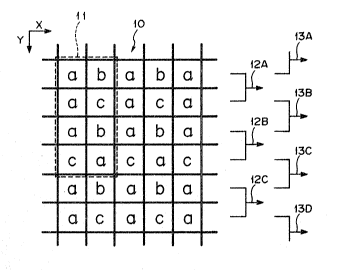
FIG. 4 shows a color filter array 10 according to this
embodiment. In this case, individual light receiving pixels of
the photo-sensitive units, 2, 4, ... of FIGS. 1 and 2 are
respectively arranged below color filters constructing the color
filter array 10.. In FIG. 4, reference numeral 11 depicts a set
of fundamental 8 pixels, and a set of fundamental 8 pixels 11 is
composed of totally 8 color filters of 2 pixels allocated to the
horizontal direction (X direction) which is the scanning
direction and 4 pixels allocated to the vertical direction (Y
dlrection). A set of fundamental 8 pixels 11 is repeated
respectively in the X direction and in the Y direction, thereby
the color filter array 10 being formed.
.
'
` 6
. ~
'~
J~
Assuming ~hat a co.l.or :ilter l of a f:i.r3t prLm~lr~ co:Lor
represents one arbitrary color of red fil-ter ~, green fil~er G
and blue filter B of three primary colors, a color filter b of a
second primary color filter represents one arbitrary color filter
of the remaining two primary ~olors and a cvlor filter c of a
third primary color repre~ents the last color filter, ~hen khe
four color filters of the left side of the fundamental 8 pixels
11 are sequentially arranged in the order of the color filter a,
the color f.ilter a, the color filter a and the color filter c
_
from above. Further, the four color filters of the right side of
the fundamental 8 pixels 11 are sequentially arranged in the
order of the color filter _, the color filter c, the color filter
_ and the color filter a from above.
However, if color filters of 2 pixels are taken out from the
X direction and color filters o 4 pixels are taken out from the
Y direction of the color filter array lO, then the 8 color
filters thus taken out can be regarded as a new set of
fundamental 8 pixels and therefore such fundamental 8 pixels have
8 expressions. As a consequence, the following blocks formed of,
for example, 8 color filters can be respectively regarded as
fundamental 8 pixels:
b a a b c a
c a c a b a
b a , a b or a c
a c a c b a
Since the color fil-ter array lO is formed by repeating the
fundamental 8 pixels, it can be considered that, regardless of
the selection of the fundamental 8 pixels, the arrangement of the
color filter array lO is the same. That is, the fundamental
pixels 11 are employed as the fundamental 8 pixels in the present
JS
:nventiorl, which ~act is equivalent to the ~act tha~ one
arbitrary expxession is selected ~rom the abo~e 8 expressions.
The scanning signal presented ~hen the color fi].ter array 10
of this embodiment is used will be described. Since the CCD
image pickup device of this embodiment i~ operated in a ield
storage fashion, one scanning signal is a mixed signa]. of irnage
pickup signals of pixels o~ two lines in the X direction.
Assuming that a certain scanning signal of, for example, an even
field is a mixed signal of 2 lines 12A, then the following
signals are mixed signals of the succeeding 2 lines 12B, 12C,
.... Then, the scanning signals of odd field are mixed signals
of 2 lines 13A, 13B, 13C, ... the phases of which are different
from those of the signals of respective 2 ].ines in the even field
by 180 degrees.
In this case, if the image pickup signal corresponding, for
example, to the color filter a is expressed by a, then the
scanning signals based on the 2 lines 12A of the even field
become 2a, b + c, 2a, b + c, ... as shown in FIG. 5A, and the
scanning signal based on the next 2 lines 12B become a + c, a +
b, a + c, a + b, ... as shown in FIG. 5B. Accordingly, i the
processing utilizing, for example, a filter circuit is employed,
then a signal proportional to (2a + b + c) is obtained from one
scanning signal in the even field by means of a low-pass filter
circuit and a signal proportional to (2a - b - c) is obtained by
means of a bandpass filter circuit. In that case, since the low
band component includes all components of the three primary
colors, such low band component can be regarded as the luminance
signal and the bandpass component can be regarded as the color
signal.
Further, a luminance signal proportional to (2a + b -~ c) is
~. ~
, ;~
-~tained from th~ ~ext scanning si-J~al of even field by ~r~earls o
a low-pass filter circuit and a color signal p~oportional to (c -
b) is obtained therefrom by means of a bandpass filter circuit.
Thereafter, these two kinds o~ signals become scannirlg signals
alternately.
In a like manner, a scanning signal based on the 2 lines 13B
of odd field become 2a, b ~ c, ..., as shown in FIG. 6A and a
scanning signal of the next 2 lines 13C becomes a ~ c, a ~ b, ...
as shown in FIG. 6B. Accordingly, also in the odd ield, the
same scanning signal as that of the even field can be obtained.
If the color filter array 10 of this embodiment is utilized
as described above, then the same scanning signals can be
obtained during the even field and odd field. Further, the
luminance signal proportional to (2a ~ b ~ c) can be obtained
from all of the scanning signals and color signals proportional
to (2a - b - c) and (c - b) can be alternately obtained from the
adjacent scanning signals. Accordingly, since different color
informations are obtained at every scanning signal, a video
signal of the NTSC system or the like can be generated by the
matrix processing similarly to the conventional case such that
the color filters of the complementary color is utilized.
Further, since the color filter array 10 of this embodiment
is constructed by the combination of only color filters R, G and
B of three primary colors, the spectral characteristic of the
color signal of the finally obtained video signal becomes -the
spectral characteristic presented on the light receiving screen
of the CCD image pickup device. There is then the advantage that
color reproducibility thereof is very excellent.
While the color filter array 10 of the embodiment of FIG. 4
is expressed in the generalized form, if the green filter G, the
. :
~ { r~ 7- ~-
j~ ~ ~o~ h l,~_Jt 3
~lue filter B and the red filter f~ are respectLve:Ly ç-~Lrlplo~ed as
the color filter ~, ~he color Eilter b ancl the color ~ilter c,
then the fundament~l 8 plxels 11 of the color filt~r a~ray 10
become as shown ln FIG. 7. If the signal is read out by
utilizing the color filtcr array ormead of fundarrlental 8 pixels
of the example of ~IG. 4 in a field storage ~ashion, then certain
scanning signals become 2G, B -~ R, ... and the next scanning
signals become G + R, B + G, ...
Accordingly, let us consider the case such that adjacent two
scanning signals are processed by using a one horizontal period
(lH) delay circuit in a matrix fashion. In this case, if the
processings expressed as
2G/2 = G
(G + R) - 2G/2 = R
(G + B) - 2Gt2 = B
are carried out, then three primary color signals R, G and B can
be reproduced. If these three primary color signals are further
processed in a color matrix processing fashion, then two color
difference signals of, for example, the NTSC system can be
reproduced with ease.
An example of an image signal processing circuit in the
image pickup device which utilizes the color filter array 10 of
the example of FIG. 4 will be described with reference to FIG. 8.
The image signal processing circuit of this embodiment is adapted
to process ad~acent two scanning signals by utilizing a lH delay
circuit where l~I represents one horizontal period.
FIG. 8 shows in block form the signal processing circuit
according to this embodiment. Referring to FIG. 8, a scanning
signal (image pickup signal) from a charge-coupled device (CCD)
14 on which the color filter array 10 is mounted is supplied
:
. . ,
~ r~ ~ 3~
~rough a sample and hold circuit 15 to arl a~l;omati-. yalrl control
(AGC) amplifier 16. An output signal from the AG~ amplifier 16
is supplied through a low-pass filter circuit 17 to a gar(~a
correction circuit 18, from which there is derived a luminance
signal Y and this lumirlance signal Y is fed to a connection
terminal 19.
The output signal of the AGC amplifier 16 is al~o supplied
directly to and through a lH delay circuik 20 to a matrix circuit
21 which then derives three primary color signals R, G and B.
The three primary color signals R, G and B from the matrix
circuit 21 are respectively supplied through white balance
amplifiers 22 to 24 and gamma correction circuits 25 to 27 to a
color matrix circuit 28 which then derives red and blue color
difference signals R-Y and B-Y. These color difference signals
R-Y and B-Y from the color matrix circuit 28 are respectively
supplied to connection terminals 29 and 30. Then, the luminance
signal Y and the color difference signals R-Y and B-Y are
processed by, for example, an NTSC encoder to provide a color
video signal of the NTSC system, though not shown.
While the present invention is applied to the CCD image
pickup device of interline transfer type which also derives a
scanning signal according to the field storage system in the
above-mentioned embodiment, the present invention is not limited
thereto and may be applied to a CCD image pickup device of frame
transfer type. Further, the present invention can be similarly
applied to a CCD image pickup device of frame storage system.
As described above, according to the present invention, the
luminance signal can be obtained from each scanning signal even
by employing the color coding based on the color filters of
primary colors, thereby different color informations being
11
~ '
~ 3.J.
^btained from each scanrlirlg s:i.grlal.
Also, according to the present invention~ a color
reproducibility can be improved as compared ~1ith the case such
that the color filter of the complementary color type is
utilized.
Having described the preferred embodiment of khe invention
with reference to the accompanying drawings, it is to be
understood that the invention is not limited to that precise
embodiment and that various changes and modifications thereof
could be effected by one skilled in the art without departing
from the spirit or scope of the novel concepts of the invention
as defined in the appended claims.