Note: Descriptions are shown in the official language in which they were submitted.
- 1 2054319
Power SUPP1Y Unit for Arc Processinq
Field of the Invention
This invention relates to a power supply unit for arc
processing. In particular, the unit is arranged such that a
commercial AC power input (single or three phase) is rectified
to DC power, and thereafter, inversely converted into a high
frequency AC by an inverter circuit. The high frequency AC
power obtained is reconverted into a power supply suitable for
arc processing through a transformer and a rectifying circuit.
Conventional arc processing power supply units will be
discussed in conjunction with the drawings.
Summary of the Invention
In accordance with one aspect of the present invention
there is provided a power supply unit for arc processing
arranged such that a three-phase or single-phase commercial AC
power, in which one of the high and low voltages of
approximately 1:2 ratio is selectively supplied, is taken as
an AC input, said AC input is, after being rectified into DC
power, inversely converted into a high frequency AC through an
inverter circuit employing switching elements, and said
inversely converted high frequency AC power is converted into
a power suitable for arc processing, which comprises: a
parallel circuit in which two or three series circuits, each
consisting of three diodes are connected in parallel in
accordance with a phase number of said commercial power
supply; input terminals of said commercial power supply, each
connected to one of the two series connection points of
respective diodes of said each series circuit; and two or
three voltage change-over circuit in accordance with number of
said series circuit, each consisting of a capacitor and a
voltage change-over switch closed at low voltage input, and
connected between the other series connection point of said
series circuit and said one series connection point of said
another series circuit adjacent to said series circuit;
wherein said inverter circuit is connected between both
terminals of said parallel circuit.
,~c,~
2 2054319
Brief Description of the Drawings
These and other objects and features of the present
invention will become clear from the following description
taken in conjunction with the preferred embodiments thereof
with reference to the accompanying drawings throughout which
like parts are designated by like reference numerals, and in
which:
Fig. 1 is a connection diagram showing an example of the
conventional apparatus;
Fig. 2 is a connection diagram showing a preferred
embodiment of the present invention;
Fig. 3 is a graph for explaining the operation of the
embodiment of Fig. 2; and
Figs. 4 to 10 are connection diagrams showing other
preferred embodiments of the present invention.
In a conventional arc processing power supply unit
used commonly for high and low voltage powers of a ratio
of approximately 1:2 such as commercial power voltages
200 V/400 V or 230 V/460 V, a power supply system that
directly transforms commercial power into a predetermined
voltage can cope with different power supply voltages by
changing the turn ratio of the transformer. Changing the turn
ratio requires that the switching elements and diodes have
dielectric strengths sufficient to withstand 400 V (or 430 V)
and capacities sufficient to withstand a large current in the
inverter and rectifying circuits. These requirements result
in a physically large and expensive circuit and offset the
effect of down-sizing the transformer and the smoothing
circuit.
In another conventional power supply system a half-bridge
(two series-connected capacitors and two switching devices)
and a full-bridge (four switching devices) type of inverter
circuit are used so that when voltage is applied to each
switching device the output voltage of the inverter circuit
may become equal.
,~
~'
3 20~31~
Fig. l is a connection diagram showing a conventional
power supply unit. The system includes rectifying diodes la,
lb, 2a, 2b, 3a, and 3b for full wave rectification of a three
phase AC power supply from input terminals U, V and W.
Capacitors 4a, 4b are used to smooth the outputs of diodes la
to 3b and serve to divide the output voltage into two partial
voltages. Switching devices 5a to 5d are connected in a
bridge with respective series-connection points thereof being
connected to a lower voltage contact point of a change-over
switch 6 and the primary winding of an output transformer 7.
The change-over switch 6 has its higher voltage contact point
connected to the series connection point of said capacitors
4a, 4b and its common contact point connected to the primary
winding of the output transformer 7. A load 8 is connected to
the secondary winding of the transformer 7. The load 8 could
be for example a rectifying circuit or an arc processing load.
In the unit of Fig. l, when the three-phase power supply
is 200 V (or 230 V), the change-over switch 6 is connected to
side (a). The switching devices 5a to 5d operate as inverters
connected in a bridge. The primary winding of the output
transformer 7 is connected between the connection point of
switching devices 5a, 5c and the connection point of switching
elements 5b, 5d. In this case, switching devices 5a and 5b,
and switching devices 5c and 5d become pairs so that the
respective switching devices in each pair are simultaneously
on-off controlled and each pair is alternately on-off
controlled by a control circuit (not shown), with capacitors
4a and 4b operating merely as smoothing capacitors.
Alternatively, when the three-phase power supply is 400 V
(or 460 V), the change-over switch 6 is connected to side (b).
In this case, the primary winding of the output transformer 7
is connected between the connection point of capacitors 4a and
4b and the connection point of switching devices 5a and 5c so
as to form a half-bridge circuit. As a result, 1/2 of the
rectifying output is applied to the transformer 7, with the
~t`: '
4 205~319
same voltage output as in the 200 V (230 V) arrangement. In
this case, switching devices 5a and 5c are on-off operated,
with devices 5b and 5d being left off.
Since the same output voltage is obtained in the inverter
circuit even when the voltage of the AC input power supply is
changed approximately at a ratio of 1:2, the dielectric
strength corresponding to the lower voltage is sufficient for
the dielectric strength of the switching device in the
inverter circuit. However, two switching devices become idle
in the case of high voltage input, and diodes la to 3b
constituting the input side rectifying circuit are required to
withstand the input voltage of 400 V and the input current of
200 V.
Furthermore, since the constitution of the inverter
circuit is changed over between a full bridge system and a
half bridge system by the change-over switch 6, the wiring for
the inverter circuit becomes long and complicated, and the
inductance and floating capacity of the wiring is increased.
Therefore, when the inverters are operated at a high
frequency, a higher surge voltage is generated at the
switching devices during on-off operation, and the capacity of
the surge absorption circuit require switching devices of a
large capacity.
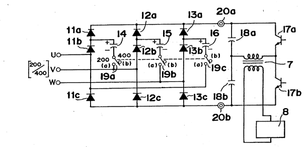
Fig. 2 shows a connection diagram of a power supply unit
of a preferred embodiment of the present invention including
diodes lla to llc, 12a to 12c, and 13a to 13c, capacitors 14
to 16, 18a and 18b, switching devices 17a and 17b, voltage
change-over switches l9a to l9c, which operate in interlock
with each other, an output transformer 7, and a load 8 of the
output transformer 7. The load 8 can be any arc load
including, a rectifying circuit, electrodes, or a low
frequency inverter circuit.
When change-over switches l9a to l9c are positioned at
side (a) (200 V, lower voltage side), a voltage doubler
rectifying circuit is constituted by diodes lla to 13c and
capacitors 14 to 16. Alternatively, when change-over switches
~~ 5 20~319
are positioned at side (b) (400 V, higher voltage side),
capacitors 14 to 16 are cut off from the circuit, and a three
phase full wave rectifying circuit is constituted by diodes
lla to 13c.
Capacitors 18a and 18b are used for dividing the
rectified output into two equal parts. The respective outputs
are then inversely converted into a high frequency AC by a
half-bridge inverter circuit constituted by switching elements
17a and 17b on-off controlled by a control circuit (not
shown). After being converted into a desired voltage by the
output transformer 7, the output is supplied to the load 8.
In Fig. 2, when change-over switches l9a to l9c are
switched to side (b) the circuit forms a normal three phase
full wave rectification circuit. The operation when change
over switches l9a to l9c are switched to side (a) will be
described with reference to the voltage waveforms of
respective phases U, V, and W shown in Fig. 3.
In period (1), the potential of U phase is the highest
and that of V phase is the lowest. Therefore, by the voltage
between U and V, the capacitor 14 is charged through the diode
llb. In this case, between the output terminals 20a and 20b,
a voltage between U and V is applied through a circuit of the
input terminal U, change-over switch l9c, capacitor 16, diode
13a, output terminal 20a, load (inverter circuit), output
terminal 20b, diode 12c, and input terminal V. Diodes lla and
12a are reversely biased by the potential capacitor 16 and U
or V and are not conductive.
The capacitor 16 has been charged ahead of this period
(period corresponding to period (5) in Fig. 3) and its
polarity is "+" at the connection point of diodes 13a and 13b,
as shown in Fig. 2, that is, the same polarity as the voltage
between U and V. Therefore, the sum of these voltage is
applied between output terminals 20a and 20b.
In period (2), the terminal voltage of the capacitor 14
is charged up to the wave-height value of the voltage between
U and V. The capacitor 14 is not further charged but is held
in this state. Since the potential of W phase is the lowest,
20~319
the sum of the voltage between W and U and a terminal voltage
of the capacitor 16 is applied between output terminals 20a
and 20b via the diode 13c in place of the diode 12c.
In period (3), the~-potential of V phase is the highest
and that of W phase is the lowest, the capacitor 15 is charged
by the voltage between V and W, and, concurrently, the sum of
the terminal voltage of the capacitor 14 and the voltage
between V and W is outputted.
In period (4), charging of the capacitor 15 is stopped,
and the sum of the terminal voltage of the capacitor 14 and
the voltage between V and U is applied between the output
terminals 20a and 20b.
In period (5), the capacitor 16 is charged by the voltage
between W and U, and the sum of the terminal voltage of the
capacitor 15 and the voltage between W and U is applied
between the output terminals 2Oa and 2Ob.
In period (6), charging of the capacitor 16 is stopped,
and the sum of the terminal voltage of the capacitor 15 and
the voltage between W and V is applied between the output
terminals 20a and 20b.
The periods (1) to (6) are rèpeated. Since, in
respective periods, the terminal voltage of respective
capacitors and the power supply voltages added thereto are of
the same polarity at all times and the output terminal 2Oa is
of positive polarity, between the output terminals 20a and
2Ob, the output voltage is equal to two times the line voltage
of the AC power supply. Therefore, when the change over
switches l9a to l9c are switched to side (a) for a low voltage
input of 200 V or 230 V, as well as to side (b) for a high
voltage input of 400 V or 460 V, the rectification output
voltage remains equal. As a result, the voltage of 400 V or
460 V at the high voltage input is rectified in full wave and
can be obtained irrespective of the power supply voltage.
For the three-phase AC power supply voltages, different
in approximately a 1:2 ratio, the rectified output is at all
times the same as the full wave rectified output voltage at
the high voltage input. This DC output is divided into two
~c
- 20~4319
equal parts, thereby to inversely convert into a high
frequency AC through a half bridge type inverter circuit.
Therefore, both the rectifying circuit and the inverter
circuit have no wastes in respect of capacity, and since the
wiring of the inverter circuit is simplified, there is no
increase the generation of surge voltage.
In the embodiment of Fig. 2, when the change-over
switches l9a to l9c are switched to side (b), the capacitors
14 to 16 are separated from the circuit. In order to use
these capacitors effectively, each side (b) contact points of
the change-over switches l9a to l9c may be connected to anodes
of diodes llc, 12c and 13c, respectively.
In the embodiment of Fig. 4, when the change-over
switches l9a to l9c are connected to side (a), it is the same
circuit as in the embodiment of Fig. 2, and when they are
connected to side (b), the capacitors 14 to 16 operate for
smoothing the DC output.
In Figs. 2 and 4, although a half bridge type inverter is
constituted as the output inverter circuit by the capacitors
18a and 18b, a full-bridge type inverter circuit composed of
four switching devices may be constituted by using voltages
between both ends of each of the capacitors 18a and 18b. In
this case, the operation is the same except that the primary
voltage applied to the output transformer 7 is two times the
voltage applied in the respective embodiments of Figs. 2
and 4.
Fig. 5 is a connection diagram of another embodiment
where the commercial AC power supply is of single phase. In
Fig. 5, the connection diagram corresponds to that obtained by
removing one phase (W phase) from the embodiment in Fig. 2,
and the same as the embodiment in Fig. 2 except that the (a)
contact point of switch l9b is connected to the connection
point of diodes llb and llc. The operation of the embodiment
in Fig. 5 is the same as that of the embodiment in Fig. 2.
Specifically, when the commercial power supply is of a high
voltage such as 400 V or 460 V, a single phase full-wave
rectifying circuit is formed by setting the change-over
,,
8 205~319
switches to side (b). Alternatively, when the commercial
power supply is of a low voltage such as 200 V or 230 V, a
single phase voltage doubler rectifying circuit is formed by
setting the change-over switches to side (a). Therefore, for
either of the input voltages of approximately 1:2 ratio, the
same DC output (voltage equal to the rectified output at the
high voltage input) is obtained between the terminals 20a
and 2Ob.
Fig. 6 is a connection diagram of another embodiment that
is arranged to be used commonly for three phase and single
phase commercial power supplies. In Fig. 6, when the input
power supply is of single phase, the power supply is connected
to 2 phases of input terminals U, V, W. The remaining one
phase is opened by a change-over switch for safety, and the
internal circuit of that phase is connected in parallel to the
other phases.
In Fig. 6, reference numeral 21 indicates a three phase
to single-phase change-over switch for changing over the input
terminal between 3-phase and single-phase. When the power
supply is single phase, switch 21 opens the terminal U and
connects the internal U terminal circuit in parallel to the
terminal W. Reference numeral 22 is a load circuit composed
of an inverter circuit, output transformer, output
rectification circuit, or arc load, which is similar to the
load in Figs. 2 and 4. Furthermore, the change-over switches
l9a to l9c are arranged to connect contact point (b) to the
output terminal 2Ob so that these change-over switches are
connected to side (b), and capacitors 14 to 16 operate as
smoothing capacitors.
In the embodiment of Fig. 6, when the 3-phase to single
phase change-over switch 21 is switched to side (A),
respective input terminals U, V, W become independent so as to
form the same circuit as in the embodiment of Fig. 4. When
the 3-phase to single phase change-over switch 21 is placed on
side (B), and change-over switches l9a to l9c are placed on
side (b) (400 V side), the single phase AC power supplied
between V and W is rectified by the full wave rectification
" ~
; .
- 9 20~319
circuit constituted by diodes 12b, 12c, and diodes 13b, 13c.
At this stage, diodes llb, and llc are connected in parallel
to the circuit of diodes 13b and 13c by switch 21 and effect
the same operation as the normal full-wave rectification
circuit.
When change-over switches l9a to l9c are on side (a)
(200 V side), voltage doubler rectifying circuit is
constituted by diodes lla to llc, diodes 12a to 12c, diode
13c, capacitors 14 and 15. In this case, when the phase of
the power supply voltage is of a positive polarity on the side
of terminal V, the capacitor 15 is charged by the voltage
between V and W through a path of terminal V, diode 12b,
capacitor 15, change-over switch l9b, and terminal W.
Simultaneously, the voltage between V and W is applied between
the output terminals 20a and 20b through a path of terminal V,
change-over switch l9a, capacitor 14, diode lla, output
terminal 20a, load 22, output terminal 20b, diode 13c (or
diode llc, switch 21), terminal W, single phase power supply
and terminal V.
Since the capacitor 14 has been charged in the polarity
indicated in Fig. 6 in the previous period, wherein the
terminal W is of positive polarity, this charged voltage and
the single phase power supply voltage are added in the same
polarity. In addition, 2 times the single phase power supply
voltage is applied between the output terminals 20a and 20b.
Subsequently, when the polarity of the AC power supply is
inverted so as to be positive on the side of terminal W, the
capacitor 14 is charged through the diode llb and
simultaneously, current flows to load 22 through a path of
terminal W, change-over switch l9b, capacitor 15, diode 12a,
output terminal 20a, load 22, output terminal 20b, diode 12c,
terminal V, single phase AC power supply and terminal W.
Since the terminal voltage of the capacitor 15 and power
supply voltage have the same polarity, as shown in
Fig. 6, these voltages are added and applied between the
output terminals 2Oa and 2Ob.
- 10 2054319
In this arrangement, when the three-phase to single phase
change-over switch 21 is changed over to side (B) (single
phase side), in the case of 200 V (or 230 V) power supply
voltage, the DC output by a voltage doubler rectifying circuit
is applied between the output terminals 20a and 20b. However,
in the case of 400 V (or 460 V) power supply voltage, the DC
voltage by the full wave rectification is supplied between the
output terminals 2Oa and 2Ob. Accordingly, irrespective of
the high or low voltage power supply, the same output voltage
can be obtained, and thereby the load circuit of the same
voltage rating can be used.
When change-over switches l9a to l9c are changed to
side (a) (low voltage side), and switch 21 is at side (B)
(single phase side), the capacitor 16 is connected in parallel
to the diode 13b irrespective of the polarity of the power
supply voltage, and does not function in the circuit, with no
charging or discharging being effected.
Fig. 7 is a connection diagram in which the positional
relation between capacitors and diodes is changed from the
arrangement shown in Fig. 4 and Fig. 8. In Figs. 7 and 8, the
operation is the same as the respective embodiments shown in
Figs. 4 and 6.
Fig. 9 is a connection diagram showing another preferred
embodiment of the present invention which is arranged to cope
with change-over between three phase and single phase and four
kinds of power supplies (three phase 200 V/400 V and single
phase 200 V/400 V) by using three kinds of change-over
switches. In particular, a three phase to single phase
change-over switch 21, a single phase 200 V to single phase
400 V or three phase change-over switch 24, and three phase
200 V to three phase 400 V or single phase change-over
switches l9a to l9c.
When the change-over switch 24 is changed to side (b)
(single phase 400 V or three phase side) and the change-over
switch 21 is changed to side (A) (three phase side), it is
suitable for use as a three phase power supply. In this
'~
11 2054319
state, when the change-over switches l9a to l9c are connected
to side (a), a circuit the same as that of the embodiment
shown in Fig. 2 is constituted, which is suitable for three
phase 200 V power supply.
However, when change-over switches l9a to l9c are changed
to side (b) (three phase 400 V or single phase side), it is
suitable for use as a three phase 400 V power supply.
When the changeover switch 21 is changed to side (B)
(single phase side) and the change-over switches l9a to l9c
are changed to side (b), it is suitable for use as a single
phase power source. In this state, when the change-over
switch 24 is connected to side (a) (single phase 200 V side),
the circuit is suitable for use as a single phase 200 V power
supply. However, when connected to side (b) (single phase
400 V or three phase side), the circuit is suitable for use as
a single phase 400 V power supply.
Consequently, in the state when the switch 24 is changed
to side (b), the change-over switch 21 is changed to side (A)
(three phase side) and switches l9a to l9c are connected to
side (a), a three phase voltage doubler rectifying circuit is
constituted by diodes lla to llc, diodes 12a to 12c, diodes
13a to 13c, and capacitors 14 to 16.
When the change-over switch 24 is changed to side (b),
the switch 21 is changed to side (A), and switches l9a to 19c
are connected to side (b), the capacitors 14 to 16 are cut off
from the circuit, and a three phase full-wave rectifying
circuit is constituted.
When the switch 21 is connected to (B) (single phase
side), the W phase input terminal is cut off. In this state,
when switches l9a to l9c are connected to side (b) and the
switch 24 is connected to side (a), a single phase voltage
doubler rectifying circuit is constituted by diodes 12a to 12c
and the capacitors 18a and 18b. Further, when the switch 24
is connected to side (b), a single phase full-wave rectifying
circuit is constituted by the diodes lla to llc and the diodes
12a to 12c.
205~319
12
As a result, by changing over change-over switches l9a
to l9c, change-over switches 21 and 24 in accordance with AC
commercial power supplies, irrespective of the three phase or
single phase of the input power supply, an approximately same
DC voltage is supplied to the load circuit 22 at input of
200 V or 400 V.
Fig. 10 is a connection diagram showing a further
embodiment of the present invention, which is arranged to cope
with four kinds of power supplies: three phase 200 V/400 V and
single phase 200 V/400 V by using switches of four steps.
Switches 25a to 25d are change-over switches of four
steps, which are interlocked with each other, and respectively
connected in series between capacitors 14, 15, 16, respective
in-series connection points of diodes 12b and 12c, diodes 13b
and 13c, diodes llb and llc, capacitors 18a and 18b, and input
terminals.
When 4-stepped switches 25a to 25d are connected to the
contact points (a) and (b), the circuit becomes the same as in
the embodiment shown in Fig. 2, and at contact point (a), the
circuit is suitable for use as a three phase 200 V power
supply. When at contact point (b), the circuit is suitable
for use as a three phase 400 V power supply.
When the 4-stepped switches 25a to 25d are connected to
contact points (c) and (d), the circuit become suitable for
use as a single phase power supply, and becomes the same
circuit as that in the embodiment shown in Fig. 6.
Specifically, the single phase power supply is connected to
input terminals U and V. In this case, when connected to
contact point (c), the circuit is suitable for use as a single
phase 200 V power supply. When connected to contact point
(d), the circuit is suitable for use as a 400 V single phase
power supply.
Therefore, when change-over switches are connected to
contact points (a), a three phase voltage doubler rectifying
circuit is constituted by diodes lla to llc, diodes 12a to
12c, diodes 13a to 13c, and capacitors 14 to 16. When the
_ 13 2 0 ~1 3 1 3
switches are connected to contact points (b), a three phase
full wave rectifier circuit is constituted with the capacitors
14 to 16 being cut off.
When the change-over switches are connected to contact
points (c), the input terminal W phase is cut off and the in
series connection point of capacitors 18a and 18b is connected
to the U phase. At this stage, a single phase voltage doubler
rectifying circuit is constituted by diodes 12a to 12c and
capacitors 18a and 18b. Furthermore, when connected to
contact points (d), a single phase full-wave rectifying
circuit is constituted by diodes lla to llc and diodes 12a
to 12c. As a result, as in the embodiment in Fig. 10, by
changing over the change-over switches 25a to 25d, an
approximately same DC voltage is supplied to the load circuit
22 irrespective of input power supply of three phase or single
phase and at input voltage of 200 V or 400 V.
Although systems of changing over the phase and voltage
of the input power supply by using change-over switches are
shown in the above embodiments, if these change-overs are not
made frequently, the circuits may be modified such that in
place of the change-over switches, respective connection
points are drawn out to a terminal board.
Furthermore, in the embodiments illustrated in Figs. 6,
8, 9 and 10, which are applicable commonly to power supplies
of three phase and single phase, the terminals to be connected
to the single phase power supply are not limited to those
illustrated. Specifically, any two terminals of the three
phase input terminals U, V, and W may be taken.
Therefore, according to the present invention, in the two
AC power supply voltages of approximately 1:2 ratio, the
rectified DC output thereof becomes, at all times, a voltage
equal to the full wave rectification voltage at the time of
high voltage input. This voltage is subsequently divided into
two equal parts by two in-series capacitors for processing by
a half bridge type inverter circuit employing two switching
elements. Alternatively, this obtained voltage may be
subsequently processed by a full bridge type inverter circuit,
_ 14 2 ~ 31 9
thereby to obtain a high frequency AC. Accordingly, it is not
necessary to increase the current and voltage ratings of the
rectifier circuit and inverter circuit wastefully. In
addition, there is no change-over circuit due to the input
power supply voltage in the inverter circuit and the circuit
becomes simple, with no increase being made in the surge
voltage during switching.
Although the present invention has been fully described
in connection with the preferred embodiments thereof with
reference to the accompanying drawings, it is to be noted that
various changes and modifications are apparent to those
skilled in the art. Such changes and modifications are to be
understood as included within the scope of the present
invention as defined by the appended claims unless they depart
therefrom.