Note: Descriptions are shown in the official language in which they were submitted.
1
20~43~"~
The present invention relates to optical
modulators, and more specifically to a technique for
linearizing the output of an external optical
intensity modulator.
Recently, there has been a growing interest in
the development of analog, amplitude modulated
optical communication systems. In comparison with
digital systems, analog communication systems
provide an efficient use of bandwidth. This is
particularly useful in cable television (CATV)
transmission system applications, where it is
necessary to transmit a large number of video
channels through an optical fiber. Compatibility
with existing equipment is achieved by using the
same signal format for optical transmission that is
in use for coaxial cable signal transmission.
In order to transmit an information signal
(e.g., a television signal) over an optical fiber, a
light beam ("carrier") must be modulated with the
information signal. The "electrooptic effect" has
been advantageously used to provide modulators for
this purpose. For example, electrooptic modulators
using miniature guiding structures are known which
operate with a low modulating power.
2~~~~~e~~l
In electrooptic modulators, the electric field
induced linear birefringence in an electrooptic
material produces a change in the refractive index
of the material which, in turn, impresses a phase
modulation upon a light beam propagating through the
material. The phase modulation is converted into
intensity modulation by the addition of polarizers
or optical circuitry. Ideally, an electrooptic
modulator should have a linear relationship between
its output optical power and the applied modulating
voltage.
In a "Mach Zehnder'° type electrooptic
modulator, an optical carrier (laser beam). is split
into two paths. At least one path is electrically
phase modulated. The two signals are then
recombined in an interferometer to provide an
intensity modulated carrier. Typically, lithium
niobate (LiNb03) is used as the electrooptic
material. Waveguides in such materials are readily
formed by titanium indiffusion.
The output power curve of a Mach Zehnder
modulator is nonlinear. Practical analog optical
communications systems, however, demand a high
linearity. See, for example, W.I. Way, "Subcarrier
Multiplexed Lightwave System Design Considerations
for Subscriber Loop Applications", J. Lightwave
Technol.,.Vol. 7, pp. 1806-1818 (1989). Modulator
nonlinearities cause unacceptable harmonic and
3
~~ ~~3 ~'~
intermodulation distortions. When it is necessary
to communicate a large number of channels, as in a
CATV application, intermodulation distortions
("IMD") can impose serious limitations on the system
performance. In principle, the second order IMD can
be filtered out if the bandwidth is less than one
octave. However, CATV transmission systems operate
with bandwidths of many octaves. The third order
IMD can only be eliminated by using devices with
,10 linear characteristics.
Injection lasers, for example, are not
perfectly linear. They can be limited by second
order or third order IMD. By using biases well
above the threshold and small optical modulation
depths, selected injection lasers can barely meet
vestigial sideband amplitude modulation CATV system
specifications. This limitation is discussed in
G.E. Bodeep and T.E. Darcie, '°Semiconductor Lasers
Versus External Modulators: A Comparison of
Nonlinear Distortion for Lightwave Subcarrier CATV
Applications", I.E.E.E. Photonics Technol. Lett.,
Vol. 1, pp. 401-403 (1989).
Electronic precompensating circuits have been
proposed to improve the linearity and reduce IMD in
laser communication systems. A quasi-linear
electrooptic modulator based on a foreshortened
directional coupler was proposed in K.T. Koai and
P.L. Liu, °'Digital and Quasi-Linear Electrooptic
4 '
Modulators Synthesized from Directional Couplers",
IEEE J. Quantum Electron., QE-12, pp. 2191-2194
(1986). Because the modulator proposed in that
article uses a short electrode in the directional
coupler, a large modulation voltage is required.
The resultant inefficiency of such a system is not '
acceptable for practical CATV signal distribution.
In another prior art system, a Mach Zehnder
interferometer with mixed transverse electric ("TE")
and transverse magnetic ("TM") polarizations was
used to cancel third order IMD. L.M. Johnson and
H.V. Roussell, "Reduction of Intermodulation
Distortion in Interferometric Optical Modulators",
Opt. Lett., Vol. 13, pp. 928-930 (1988). This
solution requires a large DC bias and an accurate
TE-TM power ratio. In addition, it suffers from low
modulation efficiency because a smaller electrooptic
term is used. The output power is the sum of two
polarization components.
It would be advantageous to provide an optical
circuit level compensation technique for linearizing
the output of an external optical intensity
modulator: It would be further advantageous to
provide such a modulator in which IMD distortions
are reduced to an acceptably low level. Such
apparatus would have particular application in
optical fiber CATV distribution systems, wherein a
plurality of television channel signals are
2~~!~~~r~
multiplexed and carried over a single fiber. It
would also be advantageous to provide such apparatus
that is economical, readily manufacturable, and
reliable. The present invention provides such
apparatus.
i
~~~~~~'l
In accordance with the present invention, an'
optical modulator comprises means for splitting an
optical signal fox communication over first and
second paths. At least the First path comprises an.
electrooptic material. An electric field of a first .
polarity is applied across the first~path to phase
modulate the signal therein. An electrooptic
directional coupler is coupled to the first and
l0 second paths. An electric field of a second
polarity opposite to the first polarity is applied
across the directional coupler to couple optical
signals from the first and second paths into. an
output signal.
Means are provided for biasing the first path
at an inflection point to provide a substantially
45° phase shift when no modulating signal is
present. The biasing means can comprise a set of
electrodes for applying an electric field across the
first path. In a preferred embodiment, the bias
field is of the same "first" polarity used for the
phase modulation.
The means for applying the first polarity
electric field can comprise a first set of
modulating signal electrodes. The means for
applying the second polarity electric field can
comprise a second set of modulating signal
electrodes. In a preferred embodiment, the optical
signal is equally split into the. first and second
paths with a Y-branch optical power splitter.
The second path of the optical modulator can
also comprise an electrooptic material. An electric
field applied across the second path will then phase
modulate the signal therein. Fhase modulation of
the signal in both the first and second paths can
provide a device with greater sensitivity.
The phase modulation provided by the first and
second polarity electric fields originates with a
common modulating signal. In a preferred
embodiment,~the magnitude of the common modulating
signal is scaled to modulate the second polarity
field at a slightly different level than the first
polarity field. This technique is used to minimize
distortions in the output signal. The directional
coupler of the preferred embodiment has a nominal
effective coupling length of ~r/4.
8
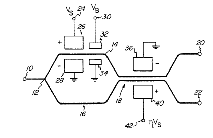
Figure 1 is a schematic diagram of a first
embodiment of the present invention wherein an
optical carrier in a first path is phase modulated
prior to an electrooptic directional couplers
Figure 2 is an alternate embodiment of the
present invention wherein the optical carrier is
phase modulated in first and second paths, prior to
an electrooptic directional coupler;
to Figure 3 is a graph illustrating the
coefficients of the second and third order terms
around the DC bias point in a modulator in
accordance with the present invention: and
Figure 4 is a graph comparing the third order
1~ harmonic distortions versus modulation depth of a
conventional Mach Zehnder interferometer to two
embodiments of a modulator in accordance with the
present invention.
9
The present invention provides a linearized
optical intensity modulator that can be fabricated
from a Y-branch optical power splitter having a
first pair of electrodes and a directional coupler
having a second pair of electrodes. The electrode
pairs are biased at opposite polarities with respect
to each other. As a result, the signal driving each
pair will have a different slope at the c~uadrature
point corresponding to the bias polarity of the
pair. Correction of harmonic nonlinearities results
from the provision of a desired couplixig coefficient
at the directional coupler. Since all compensation
is provided in a single substrate, a low cost device
is obtained.
Figure 1 illustrates a first embodiment of a
linear electrooptic modulator in accordance with the
present invention. An optical carrier (e. g., laser
beam) is input at a terminal 10 and split by a Y-
branch optical power splitter 12 into a first path
14 and a second path 16. A pair of modulation
signal electrodes 26, 2S provides an electric field
across first path 24 when a modulating signal VS is
input at terminal 24. The field across first path
14 will have a first polarity as indicated in Figure
1. A separate pair of bias electrodes 32, 34 is
provided to establish a bias field across first path
14 upon the application of a bias voltage VB at
terminal 30. The bias voltage biases first path 14
10
at the inflection point of ~/4 (i.e., to provide a
45° phase shift to the optical signal propagating
therethrough).
A directional coupler generally designated 18
couples light from the first and second paths 14, 16
respectively for output at terminals 20, 22. Like
first path 14, the directional coupler is fabricated
from an electrooptic material that responds to an
electric field provided thereacross. The electric
field is provided by a pair of electrodes 36, 40.
The modulating signal VS scaled by a factor n is
input at terminal 42 to provide an electric field
across the directional coupler at a polarity
opposite to the electric field across first path 14.
Figure 2 illustrates an alternate embodiment of
the present invention wherein an electric field is
provided across second path 16 of the Mach Zehnder
modulator by additional electrodes 29, 35. Input of
the signal voltage VS at terminal 31 establishes a '
field between electrode 28a and electrode 29 having
the polarity indicated. Second path 16 is biased by
an electric field between electrodes 34a and 35 when
the bias voltage ~~B is input to terminal 37. The
provision of electrodes adjacent both the first and
second paths provides a modulator having greater
sensitivity.
Those skilled in the art will appreciate that
the modulator of the present invention is
11 ~~~~~~"~
essentially a, Mach Zehnder modulator followed by a
directional coupler. Each device is separately
known in the art. See,,e.g., the article to Koai
and Liu referred to above. In accordance with the
present invention, these devices are combined into a
novel structure wherein a common modulating signal
is applied to both devices via separate electrodes
and at opposite polarities. The use of separate DC
bias electrodes 32, 34 on the Mach Zehnder portion
avoids heating in the main electrode 26. The
separate biasing electrodes do not require a
termination resistor, and therefore anly a minimal
amount of power is consumed as compared to the
alternative of applying the bias voltage together
with the signal voltage to electrode 26.
The Mach Zehnder portion of the present
modulator has the following response:
I = IQcos2 ( Q ~iL) ,
where 2 /,.SQL is the phase difference between the
signals in paths 14 and 16. Io is the input optical
power. The directional coupler portion of the
modulator provides:
k2
I = Io sin2 ( kz + L»ZL) ,
]CZ -i- Q~~
CA 02054337 1999-10-20
12
where k is the coupling constant, L is the length,
and p p = (p~ - pZ)~ 2 ,p~ and ,BZ are the wave vectors
in the two waveguides. Biased at the inflection
point of ~r/4, each portion taken separately can
provide a null for the second harmonic and
intermodulation distortions. However, the third
harmonic and intermodulation distortions are at or
near their maxima in conventional separate Mach
Zehnder and directional coupler devices.
In accordance with the present invention, Y-
branch optical power splitter 12 divides the optical
power at terminal 10 equally into two arms of the
Mach Zehnder modulator, which operates as a phase
shifter. The directional coupler that follows the
Mach Zehnder modulator has a nominal coupling
constant length product kL, of ~r/4, i.e., half a
coupling length. The output can be taken from
either of the two output waveguides at terminals 20,
22. The modulation signal applied to the phase
shifter produces a p~B. The same modulation signal
with a reversed polarity and a multiplication
factor, r~, is applied to the directional coupler.
This multiplication factor can be optimized for
minimal distortions according to the value of kL.
The output can be written as:
I=Io f as «~ ( x-,p R ) +az ( x- p ~ ) z+a3 ( x-Q R ) 3+a4 ( x-p R ) 4+a5 ( x-
p R ) 5+ . . . )
13
where Io represents the input power, x is the AC
modulation signal, and DAB is essentially the DC
bias. The coefficient of the linear term determines
the efficiency of the modulator.
The coefficients of the second order and the
third order terms for the modulator of Figure 2 are
shown in Figure 3 as a function of O p. The
directional coupler section is assumed to have kL =
n/4. n is assumed tn be 0.947. As shown in Figure
3, bath the second order term 60 (represented by
circles) and the third order term 62 (represented by
dots) are zero or near zero at O ~ = 0. It should
be appreciated that there are other combinations of
kL and r~ which can also provide~nulled second order
and third order terms. Depending on the values of r~
and kL used, the coefficient of the third order term
may be zero at one or two values of D p.
In comparison with a Mach Zehnder
interferometer, the present modulator, using optimal
kL and r~, requires over twice the modulation voltage
magnitude to obtain a similar modulation depth.
However, the third order harmonic and
intermodulation distortions are orders of magnitude
lower than those of a conventional Mach Zehnder
interferometer.
When modulated by a sinusoidal signal, the
harmonic contents in the output of a modulator
constructed in accordance with the present invention
w.
%.
14
can be found by computing a fast Fourier transform.
Figure 4 illustrates the third harmonic distortions,
defined as 20 log (harmonic content/linear term),
versus the optical modulation depth for a
conventional Mach Zehnder interferometer (solid
curve 70) and for two different linear modulators in
accordance with the present invention. One such
modulator, represented by curve 72, has kL = 0.2~r
and n = 1.281. The other modulator, represented by
curve 74, has kL = ~r/4 and r~ = 0.95. When the
modulation signal consists of two tones, IMD is
present in addition to harmonic distortions. With
the same modulation depth for both tones,, the third
order IMD is three times (i.e, 9.54 dB higher than)
the third order harmonic distortion plotted in
Figure 4. Assuming that a -95 dB third order IMD is
required for CATV applications, the optical
modulation depth available from the linear modulator
of the present invention is 13% for kL = ~r/4 and 8%
for kL = 0.2~r. The Mach Zehnder interferometer
alone can only offer an optical modulation depth of
1.3%. Among combinations of kL and r~ tested, the
largest optical modulation depth, which can be
obtained by using kL = 0.988 and ~7 = 0.629, is 16%.
Results shown in Figure 4 indicate that it is not
necessary to have kL = ~r/4. Any deviation can be
partially compensated for by adjusting r~. However,
the modulation efficiency may be further reduced.
15
For example, if kL = 0.2n, the modulation voltage is
increased by a factor of 1.47 in comparison with kL
= r~/4. Distortions are also larger as shown in
Figure 4. The dips in Figure 4 result from details
in the dependence of the third order coefficient a3
on p (3. The positions of these dips can be varied.
Fox a given kL, by tuning r~, one of the dips can be
moved to a larger modulation depth. In other words,
the distortion performance can be improved at large
modulation depths if a slight deterioration in the
distortion performance at small modulation depths
can be tolerated. The second order distortions of
such electrooptic modulators are always below -120
dB when they are biased at their inflection points.
It is noted that the value of r~ (which
establishes the scaling of the modulating signal
applied to the directional coupler electrodes) must
be tightly controlled. A deviation of just 2.5%
from the optimal value can increase the third order
distortions by 20 dB.
It should now be appreciated that the present
invention provides a linear electrooptic external
amplitude modulator. Both the second order and
third order terms can be nulled simultaneously at
zero DC bias. Second order distortions are well
below those reguired for CATV transmission systems.
With an optical modulation depth of up to 16% for
each channel, third order IMD on the order of -95 dB
16
~~~ a«.~~~~
is achievable. The use of an electrooptic modulator
as described in conjunction with diode-pumped solid
state lasers provides superiox performance than
directly modulated injection lasers for CATV
applications.
Although the invention has been described in
connection with several preferred embodiments, those
skilled in the art will appreciate that numerous
adaptations and modifications can be made thereto
without departing from the spirit and scope of the
invention, as set forth in the following claims.