Note: Descriptions are shown in the official language in which they were submitted.
,3 1 ,J
CONSTANT FREQUENCY RESONANT DC/DC CON~/kK l ~K
Field of the Invention
This invention generally relates to resonant dc/dc converters.
More specifically, it is directed to pulse width modulation (PWM) resonant
mode dc/dc converters with constant and very high operating frequency.
Ba~gloulld of the Il~v~l~lion
In many advanced telecommunication systems, for example,
such as Fiber World Products, high performance dc/dc power converters with
low voltage, high current output are required. Some of the basic
requirements for these power converters are:
a) high ~ffil~iency;
b) high power density;
c) high reliability;
d) fast dynamic response;
e) low mass densit,v;
fl low EMI (both conducted and radiated);
g) regulated output dc voltage with low ripple; and
h) constant frequenc,v operation.
It is believed that the above features of the converters will
25 ~ignifil~ntly enh~nce overall ~elroll.,ance of the system. Consequently, there
is likely to be a trend toward use of such converters in the future.
Various topologies of half-bridge resonant converters are studied
and compared in IEEE Trans. on Power Electronics, Vol. 3, No. 2, April 1988,
30 pp. 174-182 "A Comparison of Half-Brldge Resonant Converter Topologies"
by R. Steigerwald. A half-bridge inverter is coupled with a series, a parallel or
a series-parallel resonant circuit and their ~uelfullLlances are compared.
3 ~ ~
In an article by the present inventor, "Performance Comparison
of Pulse Width Modulated Resonant Mode dc/dc Converters for Space
Applications", IEEE Industry Applications Society Conference Record, Oct.
1989, pp. 1106-1114, full-bridge resonant converters are described.
PWM series-parallel resonant converters are further studied in
"Fixed Frequency PWM Series-Parallel Resonant Converter", by A.K.S. Bhat,
IEEE Industry Applications Society Conference Record, Oct. 1989, pp. 111
1121.
U.S. Patent 4,857,822, issued August 15, 1989 in the name of
Tabisz et al, describes a zero-voltage-switched multi-resonant converter in
which a multi-resonant switch forms three different resonant circuits for
improved performance at higher freq1len~i~s
U.S. Patent 4,833,584, issued May 23, 1989 in the name of Divan,
on the other hand, teaches a high frequency quasi-resonant current mode
static power conv~llel in which the output voltage is controlled by varying
the operating frequency. It is therefore not suitable for the application where
20 frequency locking/synchronization is required.
In the above articles, parallel resonant and series-parallel
resonant circuits contain only parallel capacitors as their parallel resonant
component.
Objects of the Invention
It is therefore an object of the present invention to provide
resonant dc/dc CO11V~
2 ~ 3 ~ cij
It is another object of the present invention to provide pulse
width modulated (PWM) resonant dc/dc converters by using phase-shift
control within the inverter.
It is a further object of the present invention to provide PWM
resonant dc/dc converters including a series and a parallel resonant circuit.
It is a further object of the present invention to provide a
resonant dc/dc converter with near zero turn-on, turn-off, and snubber losses
10 while operating at constant and very high frequency.
Summary of the Invention
Briefly stated, the present invention is directed to a constant
15 frequency full resonant mode dc/dc converter which comprises a full bridge
inverter, a resonant circuit means connected to the full bridge inverter, a
transformer connecte-3 to the resonant circuit means, and a rectifying circuit
means col necte~ to the` transformer. The resonant circuit means includes a
parallel resonant branch which has a parallel inductor and a parallel capacitor,20 and a series resonant branch which has a series inductor.
Brief Des.~ Iion of the Dld~. ings
For a more complete underst~n~ing of the present invention
25 and for further objects and advantages thereof, reference may now be made to
the following description, taken in conjunction with the accompanying
drawings, in which:
Figure 1 is a diagrammatic illustration of a prior art dc/dc
converter;
Figure 2 is a diagrammatic illustration of a resonant dc/dc
converter according to one embodiment of the present invention;
2 ~
Figures 3(a) and 3(b) are graphs showing various waveforms of
signals on a corresponding time scale;
Figure 4 is a diagrammatic illustration of a resonsant dc/dc
converter according to a further embodiment of the present invention; and
Figures 5 and 6 are graphs showing various wavefo~ s of signals
according to the embodiment shown in Figure 4.
Detailed Descl;~tioll of the P~ d Embodiments
o A large number of resonant mode dc/dc converter topologies
have been reported in the literature. However, it has been shown, for
example, in the aforementioned articles that the series-parallel resonant
converter is most suitable for applications with low voltage, high current
regulated dc outputs.
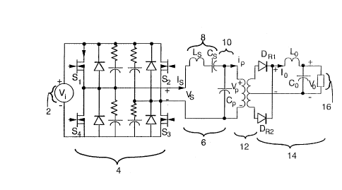
Figure 1 illustrates diagrammatically such a known dc/dc
converter circuit. In the figure, a dc voltage source 2 supplies the power to a
full-bridge in~rerter 4 whose output, voltage Vs and current Is is fed to a
resonant circuit means 6. The resonant circuit means consists of a series
resonant branch 8 and.a parallel resonant branch 10. A transformer 12 is
connected to the resonant circuit means. The secondary windings of the
transformer is provided with a full-wave rectifying circuit means 14 which
feeds its output to a load 16.
It has been well known that the full-bridge inverter contains
switching elements, e.g. FETs Sl, S2, S3 and S4 and their parallel or anti-
parallel diodes. Snubber capacitors and resistors are also provided across theirrespective switching elements. The full-wave rectifying circuit means
includes rectifying diodes and a filter consisting of a capacitor and an inductor.
In the circuit shown, the output voltage of the converter can be
regulated by varying either (a) switching frequency of the converter with
respect to the resonant frequency at constant pulse width, or (b) pulse width ofthe converter at constant switching frequency. Between the two, it has been
5 shown that the pulse width modulation (PWM) at constant switching
frequency performs better than the variable frequency method, particularly in
systems with frequency locking requirement. However, the PWM method
also has the following disadvantages:
(1) turn-on losses (for either switches S1 and S4 or switches S2
and S3) and turn-o~f losses (for either switches S2 and S3 or
switches S1 and S4) are present which are dnmin~nt at
higher o~elatil~g freq~enri~si
(2) lossy snubbers are required across switches S1 through S4.
These losses increase as the operating frequency of the
converter is increased;
(3) either pair of switches S1 and S4 or S2 and S3 experience
high`di/dt and dv/dt switching stresses; and
(4) fast recovery diodes are required across either pair of
switches S2 and S3 or Sl and S4~
",
All the above disadvantages of the pulse width modulation limit
the operation of the converter at m~dillm freql~enries (up to approximAtely 40
kHz).
Referring to Figure 2, one of the plefelled embodiments is
diagrAmmAtically illustrated. The full-bridge inverter 22 contains four
switches (Sl to S4), four diodes (D1 to D4) and four snubber capacitors (C1 to C4).
In this embo~limen~, high frequency MOSFET switches are employed for S1 to
S4 and no external diode is required across the switch as body diodes of the
30 MOSFETs serve the function for D~ to D4. The function of this bridge is to
, : .
~ ~3 ~
convert dc input voltage to high frequency quasi-square waveform voltage Vs
at its own output.
The resonant circuit means 24 consists of a series branch 26 and a
5 parallel branch 28. The series and parallel branches of the resonant circuit
means each comprise an inductor and a capacitor. Thus, a series capacitor Cs
and a series inductor Ls are in series in the series branch and a parallel
capacitor Cp and a parallel inductor Lp are in parallel in the parallel branch.
The components of the resonant circuit means are selected so that a close-to-
o sinusoidal voltage waveform Vp across the parallel branch, and a near-
sinusoidal current waveform Is with lagging power factor through the series
branch is obtained.
The high frequency transformer 30 provides matching and
15 isolation for the output voltage of the converter. The rectifying circuit means
32 includes rectifying diodes ~RI and DR2~ and a filter consisting of an inductor
Lo and capacitor CO so that an essentially ripple-free dc output voltage VO is
applied to the load 34.
In another embodiment, the parallel inductor Lp of the parallel
branch of the resonant circuit can be included as an integral part of the high
frequency transformer 30 by adjusting the parameters of the transformer, such
as air gap, turns, etc.
In this converter, a high frequency quasi-square voltage
waveform is produced at the output of the full-bridge inverter 22 using phase-
shift control within the inverter. The components of the series branch are
tuned to the operating frequency so that this branch provides a zero
impedance at the fundamental operating frequency. The components of the
30 parallel branch are off-tuned such that this branch provides an effective
inductive impedance at the filnli~m~nt~l operating frequency.
2~4'~
The application of the high frequency quasi-square voltage
waveform across the combination of series and parallel branches results in a
near-sinusoidal curren~ waveform with lagging power factor through the
series branch and a close-to-sinusoidal voltage waveform across the parallel
5 branch. Voltage and current wave sh~ping obtained in this way achieves the
following:
a) load-independent output voltage resulting in a narrow
range of phase-shift control;
b) maximum voltage gain of the converter resulting in
lower conduction losses;
c) turn-on and turn-off of the MOSFET switches under zero
voltage, resulting in near zero switching losses;
d) loss-less snubbers across the switches;
e) elimination of Miller's effect, res-llting in lower gate drive
current and losses at MOSFET switches;
f) mAxim1lm duty cycle (50%) for each rectifying diode of the
output re~ ing circuit means, resulting in a lower value
of the output filter in~1llctor; and
low voltage stress across the output rectifying diode,
res~lting in the use of schottky diode with lower ~o~ard
voltage drop and hence co~duction losses.
The sinusoidal voltage waveform Vp across the parallel branch
also appears at the primary winding of the transformer 30. The rectification
,
25 achon of the output rectifying diodes converts this sinusoidal voltage
~vdve~",. into unidirectional output voltage waveform VDR at the output of
; ~ the output filter. The required voltage is now filtered by the output filter to
provide a low ripple output dc voltage VO. The output voltage of the
col~vl:lter is m~intained constant at a desired level against any variation in
~. ~
30 input voltage and output load by controlling the phase shift angle of the
~, ~
.
- :,
converter. This converter performs at the operating frequency up to several
hundred kHz.
A description of the operation of the dc/dc converter shown in
5 Figure 2 will now be given with reference to Figure 3.
For a steady-state cycle, there exists eight distinct intervals in
which the converter of Figure 2 operates. For each interval, the operation of
the converter is described below, where gating signals igl, ig2, ig3 and ig4 are10 control signals applied to the gates of the MOSFET switches S1, S2, S3 and S4 respectively.
Interval I:
During this interval, MOS~ET switches Sl and S~ are conducting
15 and carrying the positive resonant current Is~ Simultaneous conduction of S1
and S2 provides a zero voltage interval for the output voltage of the inverter
(Vs)~ The zero voltage interval is needed to control power flow from the
input to the output in order to regulate and/or vary the output DC voltage.
20 Interval II:
At the beginning of thls interval, gating signal igl applied to the
gate of switch Sl has been removed. Switch Sl starts to turn-off, and the
snubber capacitor Cl starts to charge. At the same time, because of the positiver~son~nt current Is~ the snubber capacitor C4 across switch S4 starts to discharge
25 to the reson~nt circuit. Once voltage across the snubber capacitor C4 reacheszero, the positive reso~ ~nt current forces anti-parallel diode D4 across switchS4 to conduct. Simultaneous conduction of diode D4 and switch S2 provides a
negative voltage Vs at the output of the inverter. Since energy stored in the
snubber capacitor is discharged to the resonant circuit, a larger value of the
~3~ 3 ~
snubber capacitor Cl is employed to provide a slow rise of the voltage across
switch Sl. This ensures a close to zero turn-off loss in the switch.
Interval III:
At the beginning of this interval, gating signal ig4 has been
applied at the gate of switch S4. The resonant current Is is now transferred to
switch S4 from anti-parallel diode D4. Since diode D4 was conducting prior to
the conduction of switch S4, turn-on of switch S4 is, therefore, obtained under
zero voltage. This results in zero turn-on loss for the switch. During this
10 interval, switches S2 and S4 conduct and a negative voltage Vs appears at theoutput of the inverter. In this interval, power flows from input DC source to
the resonant circuit.
Interval IV:
: 15 At the beginning of this interval, gating signal i~2 from the gate
of switch S2 has been removed. Switch S2 starts to turn-off, and the snubber
capacitor C2 starts to charge. At the same time, because of the negative
resonant current Is~ the snubber capacitor C3 across switch S3, starts to
discharge to the resonAnt circuit. Once voltage across snubber capacitor C3
reaches zero, the negative rçson~nt current forces anti-parallel diode D3 to
conduct. Simultaneous conduction of switch S4 and anti-parallel diode D3
provides a zero voltage interval for the inverter output voltage Vs. A large
value of snubber capacitor C2 across switch S2 provides a slow rise of voltage
across switch S2, thereby ~liminA~ing turn-off loss in the switch.
Interval V:
At the beginning of this interval, gating signal ig3 has been
applied at the gate of switch S3. The resonant current Is is now transferred to
switch S3 from anti-parallel diode D3. Since diode D3 was conducting prior to
the conduction of switch S3, turn-on of the switch is, therefore, obtained
~, ~
~ s ? . ~
under zero voltage which results in zero turn-on loss for the switch~ During
this interval, switches S4 and S3 are conducting and providing a zero voltage
interval for the inverter output voltage V
5 Interval VI:
At the beginning of this interval, gating signal ig4 from the gate
of switch S4 has been removed. Switch S4 starts to turn-off and snubber
capacitor C4 starts to charge. At the same time, because of negative resonant
current Is~ the snubber capacitor Cl across switch S1 starts to discharge to theresonant circuit. Once voltage across snubber capacitor C1 reaches to zero, the
negative resonant current forces anti-parallel diode D1 to conduct.
Simultaneous conduction of diode D1 and switch S3 provides a positive
voltage Vs at the output of the inverter. A large value of snubber capacitor C4
provides a slow rise of voltage across switch S4, thereby eliminating turn-off
5 loss in the switch.
Interval VII:
At the beginning of this interval, signal ig1 has been applied at
the gate of switch S1. The resonant current Is is now transferred to switch S1
20 from anti-parallel diode D1. Since diode D1 was conducting prior to the
conduction of switch S1, turn-on of switch S1 is achieved under zero voltage,
thereby elimin~ting turn-on loss for the switch. During this interval,
switches S1 and S3 are con~l-cfing and providing a negative voltage Vs at the
output of the inverter.
Interval VIII:
At the beginning of this interval, gating signal i~;3 from the gate
of switch S3 has been removed. Switch S3 starts to turn-off, and snubber C3
starts to charge. At the same time, because of positive resonant current Is~ the30 snubber capacitor C2 starts to discharge to the resonant circuit. Once voltage
across snubber capacitor C2 reaches zero, the positive resonant current forces
anti-parallel diode D~ to conduct. Simultaneous conduction of switch S1 and
diode D2 provides a zero voltage interval for the inverter output voltage Vs.
A large value of snubber capacitor C3 provides a slow rise of voltage across
5 switch S3, thereby eliminating turn-off loss in the switch.
At the position where ~ot = 2~, ~O is the filnd~mPntal operating
frequency in radian/second, gating signal ig2 is applied at the gate of switch S2.
Switch S1 and S2 now conduct simultaneously and a new cycle begins.
The above description of the convelle operation reveals that the
switches are always turned-on and turned-off under near zero voltage,
thereby eliminating the switching losses. Further, the snubber capacitors
always discharge to the resol ~nt circuit, which also eliminates the snubber
15 losses. As can be seen in the above from the above discussion with reference
to the operation of the converter, all this is possible because of the lagging
nature of the reson~nt current Is and large values of snubber ~ra~itors. The
resonant circuit employed in this converter provides the desired type of
output current Is.
The table below shows effi.i~ncies for the converter circuits of
Figures 1 (prior art) and 2 (invention) as a function of operating frequency. Ascan be seen from this table, the P~ iency of the converter circuit of Figure 1
decreases as the ope,ating frequency increases, while the efficiency of the
25 convellel circuit of Figure 2 is independent of the operating frequency and is
always higher than the other circuit. This gives the obvious advantages of the
conve~ circuit of Figure 2 over the collv~l~er circuit of Figure 1 for high
- ~ frequency operation in terms of higher power density and lower conversion
losses.
,
'
, ~
OPERATING EFFI~ NC:Y OPERATING
r~ PARAMETERS
PRIOR ART~ hv ~ n ~ lON
2S kHz 87 . 0% B7 .1% Oul.~u~.
Voltage - 5V
50 kHz 85.0~ 87.1% Oul~ul. Power
~ 500W
100 kHs 83 . o% 87 .1% Input Vo1t-
~IgQ ~ 48V
250 XHZ 76.3% a7.1
500 k~z 67 . 29~ ~7 . 19
1000 kHz s5. o% 87 . 19~
Referring now to Figure 4, a further embodiment of the present
invention is diagrammatically illustrated. In this figure, the resonant circuit
5 means 40 consists of a series branch 42 cont~ining a series inductor Ls and a
parallel branch 44 cont~ining a combination of a parallel inductor Lp and a
parallel capacitor Cp. The components of the parallel branch are s~lecte~l such
that they are tuned to the operating frequency of the converter. However, the
value of the series inductor Ls is chosen such that the reson~nt frequency of Ls10 and Cp is about 1.7 times the operating frequency of the converter. The series
in~ ctor Ls has two function~: (a) it provides high impe~nces for harmonic
components which are present in output voltage of the full-bridge inverter,
and (b) it limits discharging from the parallel capacitor to the switches of thefull-bridge il~Vel Lel during zero voltage interval of the output voltage of the5 full-bridge il~veller. The parallel inductor Lp and parallel capacitor Cp of the
parallel branch also have two functions: (a) they provide a near-sinusoidal
stiff voltage source across the output transformer, and (b) they allow the
circ~ tin~ current of the resonant circuit to be confined primarily within the
parallel branch.
In this converter, a high frequency quasi-square voltage
~averorll~ is produced at the input of the resonant circuit means using phase-
shift modulation within the inverter. This voltage contains f~m~l~ental
2 ~j 3 ~
and odd harmonic components. The series inductor Ls of the series resonant
branch offers a low impedance for the flln~lAnl~n~l, and high impe~l~ncPs for
the harmonic components of the output voltage. The parallel inductor Lp
and parallel capacitor Cp, which are tuned to the operating frequency, provide
5 a high impedance for the f1ln~1Ament~l, and low impe-l~nces for the harmonic
components of the output voltage. Applic~tion of the high frequency quasi-
square voltage waveform across the combination of series and parallel
branches results in a resonant current waveform which has near
exporlenti~lly rising and falling edges with lagging power factor through the
10 series inductor and a near-sinusoidal voltage waveform cross the parallel
branch. Voltage and current wave shaping obtained in this way achieves the
following characteristics, in addition to some features discussed heretofor
with respect to the embodiment shown in Figure 2:
a) circulating currents are cot fine-l within the parallel
5 branch, resulting in high convelle~ Pffi~iPncy from full-load to reduced-load; and
b) turn~on and turn-off of the MOSFET switches under zero
voltage over a wide range of phase-shift control, resulting in near zero
switching losses.
It is therefore evident that the switches are always turned on and
turned off under near zero voltage, thereby eliminating the switching losses.
Further, the cnllhbPr capacitors always discharge to the resonant circuit, whichalso elimin~tes the snubber losses. In achieving near zero switching and
25 snubber losses, shape of the output current waveform Is plays a major role.
The nature of current Is should be such that it must force the anti-parallel
diode across the switch to conduct before the switch can be turned on. This
will ensure discharging of the snubber capacitors to the resonant circuit, and
~ ~turn-on of the switches under zero voltage. As explained earlier, the
; ~30 components Lp and Cp of the parallel branch are tuned to the operating
frequency. However, the value of the series inductor is chosen such that the
~:
2 i.~
resonant frequency of Ls and Cp is higher than the operating frequency of the
converter. The resonant frequency of Ls and Cp has a signific~nt effect on the
shape of resonant current waveform Is as shown in Figures 5 and 6. As can be
seen from these figures, depending on the values of the resonant frequency,
5 the current Is may have multiple or single zero crossings in each half cycle.
Over a wide range of control of the pulse width angle (~), the current
waveform with multiple zero crossings does not always ensure conduction of
the anti-parallel diode before the switch across it is turned on. Therefore, theresonant frequency of Ls and Cp should be such that the resultant output
10 current waveform has only single zero crossing in each half cycle over a widerange of the angle ~ control. Normally the resonant frequency of Ls and Cp is
chosen about 1.7 times the operating frequency of the converter.