Note: Descriptions are shown in the official language in which they were submitted.
2054~92
. 1
PLUG AND RECEPTACLE OF A MICROSTRIP LINE CONNECTOR
BACKGROUND OF THE INVENTION
The present invention relates to a plug and a
receptacle of a connector by which microstrip lines
formed on separate printed circuit boards to constitute
high-frequency circuits can electrically be connected to
and, if necessary, disconnected from each other.
In circuits handling signals of an ultrahigh
frequency band a circuit pattern which is formed on a
printed circuit board has a microstrip line structure on
account of impedance matching. Where it is necessary
that circuits formed by microstrip lines be separately
mounted on a plurality of printed circuit boards, it is
customary in the art to mount coaxial connectors to the
microstrip lines and interconnect the coaxial connectors
by coaxial cables to interconnect the microstrip lines
of the separate printed circuit boards.
Since the coaxial connector is bulky as well as
expensive, a large space is required for interconnecting
the printed circuit boards. This introduces difficulty
in miniaturization of the entire device. In view of
this, it is considered to employ a connector which
permits electrically direct connection of printed circuit
boards, but the connector of this type has a high
impedance, which mismatches with the microstrip line.
If such a connector is used with ultrahigh frequency
circuits, then a reflection occurs in the connector,
resulting in deterioration of the signal quality. In
the case of directly interconnecting printed circuit
boards, particularly close tolerances are needed for
positioning them relative to each other, so that their
connection may sometimes become difficult. To avoid
2 20S~5~2
this, it is necessary to increase the widths and lengths
of signal contacts and ground contacts of the connector,
but this increases the inductance of the connector, and
hence augments the impedance mismatching.
SUMMARY OF THE INVENTION
It is therefore an object of the present
invention to provide a plug and a receptacle of a
connector for a microstrip line which are able to
directly interconnect printed circuit boards while
maintaining impedance matching with the microstrip line.
The plug of a connector for a microstrip line
according to the present invention is made up of: a
ground contact member provided with a coupling plate/
disposed astride a signal conductor forming a strip line
on a printed circuit board and having a recess formed in
a manner to avoid contact with the signal conductor, and
a pair of contact pieces projected from opposite ends of
the coupling plate in a direction vertical to the surface
of an insulating plate of the printed circuit board where
the strip line is formed; a signal contact member
provided with a contact piece disposed just midway
between the pair of contact pieces of the ground contact
member and held in contact with the signal conductor of
the strip line, and a contact bent at right angles to
the contact piece and projected therefrom in parallel
to the contact pieces of the ground contact member; and
an insulating support block electrically isolating but
supporting the signal contact member and the ground
contact member as one piece.
The receptacle of the present invention, for
receiving the plug, is made up of: a substantially
rectangular parallelpipedic insulating housing provided
with both side panels each having cut therein a groove
20545~2
for receiving one of the pair of contact pieces of the
ground contact member of the plug, a front panel having
made therein a contact receiving hole substantially at
the center of a line joining the openings of the grooves,
and a top panel formed as a unitary structure with the
both side panels and the front panel; a signal socket
contact including contact piece means housed in the
insulating housing at the axial position of the contact
receiving hole for elastic contact with the signal
contact of the plug, and an extended piece extended from
the base of the contact piece means along the top panel
of the housing and having a predetermined area; a ground
socket contact housed in the insulating housing and
exposed in the grooves cut in the both side panels for
contact with the pair of contact pieces of the ground
contact member of the plug; and a shield cover which is
electrically connected to the ground socket contact,
surrounds and shields the ground socket contact and the
signal socket contact, forms an electrostatic capacitance
between the extended piece of the signal socket contact
and the signal socket contact and is connected to a
ground conductor of the microstrip line.
The plug and the receptacle according to the
present invention are electrically and mechanically
connected to strip lines formed on printed circuit
boards, respectively, and by putting the plug in the
receptacle, the strip lines formed on the separate
printed circuit boards can be interconnected directly.
In addition, the receptacle includes the piece extended
from the signal socket contact in parallel to the shield
cover, by which an appropriate electrostatic capacitance
can be formed between the signal socket contact and the
shield cover, and by a suitable selection of the
4 2054592
electrostatic capacitance, the impedance between the
signal socket contact and the shield cover can be set
to a proper value. Thus, the impedance of the connector
can be matched with the impedance of the microstrip line;
namely, impedance matching can be achieved. Accordingly,
the printed circuit boards can be directly interconnected
and the impedance of their connecting portion can be
matched with the impedance of the microstrip line.
BRIEF DESCRIPTION OF THE DRAWINGS
Fig. 1 is a perspective view for explaining the
construction of the plug according to the present
invention;
Fig. 2 is a perspective view for explaining the
construction of a ground contact member for use in the
plug of the present invention;
Fig. 3 is a perspective v-iew for explaining the
shape of a signal contact member for use in the plug of
the present invention;
Fig. 4 is a vertical sectional view for
explaining how to engage the plug and the receptacle
according to the present invention;
Fig. 5 is a perspective view for explaining the
construction of the receptacle according to the present
invention;
Fig. 6 is a horizontal sectional view for
explaining how to engage the plug and receptacle
according to the present invention;
Fig. 7 is a perspective view for explaining the
construction of a signal socket contact for use in the
plug according to the present invention;
Fig. 8 is a perspective view for explaining the
construction of a ground socket contact for use in the
plug of the present invention;
2054592
Fig. 9 is a perspective view for explaining the
construction of a shield cover for use in the plug of
the present invention; and
Fig. 10 is a perspective view of the receptacle
5 as viewed from the back thereof. I
DESCRIPTION OF THE PREFERRED EMBODIMENTS
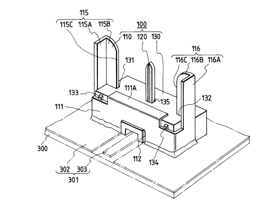
In Fig. 1, reference numeral 100 indicates
generally a plug of a connector for a microstrip line
in accordance with an embodiment of the present
invention.
The plug 100 comprises a ground contact member
100, a signal contact member 120 and an insulating
support block 130. Fig. 1 shows the plug 100 on the
assumption that it is mounted on a printed circuit board
300. The printed circuit board 300 in this example is
shown to have formed thereon an open planar microstrip
line 301. That is, the microstrip line 301 is composed
of a ground conductor 302 and a signal conductor 303
formed in the same plane.
The ground contact member 110 is electrically
connected to the ground conductor 302 forming the
microstrip line 301 and is mounted on the printed circuit
board 300. A portion of the ground contact member 110
making contact with the ground conductor 302 will
hereinafter be referred to as a coupling plate portion
111. The ground contact member 110 is obtained by
punching out a sheet metal into a desired pattern and
bendin8 it as required. The ground contact member 110
includes the coupling plate portion 111 which covers one
longer side surface of the substantially rectangular
parallelpipedic insulating support block 130 and has its
both end portions bent in a manner to hold therebetween
the insulating support block 130 on its opposite end
2~54~92
faces (i.e. shorter side surfaces) L-angle brackets 115
and 116 coupled at their lower ends to both ends of the
coupling plate portion 111 and extending upwardly of the
top of the insulating support block 130 on its both end
faces. The L-angle brackets 115 and 116 have their plate
portions 115A and 116A held in contact with the shorter
side surfaces of the insulating support block 130, and
plate portions 115B and 116B bent at right angles to
the plate portions 115A and 116A, respectively, are
substantially flush with each other and are received in
grooves 131 and 132 cut in the shorter side surfaces of
the insulating support block 130. The coupling plate
portion lll has a recess 112 cut in its lower marginal
edge centrally thereof so that it remains out of contact
with the signal conductor 303 forming the microstrip
line 301.
The coupling plate portion lll has its upper
central marginal portion bent at right angles to form a
press piece lllA. The coupling plate portion lll has
downward projecting pieces 113 and 114 extending from
its both ends in the direction opposite from the L-angle
brackets 115 and 116 (Fig. 2). The projecting pieces 113
and 114 are pressed into holes made in the printed
circuit board 300 so that the plug lO0 is mechanically
planted thereon. The coupling plate portion lll is
soldered along its lower marginal edge to the ground
conductor 302 of the microstrip line 301, and hence is
fixed thereto electrically and mechanically. The plate
portions 115B and 116B of the L-angle brackets 115 and
116 form contact piece portions and their opposed edges
115C and 116C make contact with a ground socket contact
of a receptacle 200 described later.
The upper marginal portion of the rectangular
~~ 7 2~545`92
parallelpipedic insulating support 130 is locked by the
press piece lllA of the coupling plate portion lll. The
contact piece portions 115B and 116B are received in the
grooves 131 and 132 cut in the both end faces of the
insulating support block 130, and lugs 133 and 134 engage
marginal edges of the coupling portion lll to prevent it
from falling off. The insulating support block 130 has a
centrally-disposed through hole 135 extending therethrough
vertically, which receives and firmly supports the signal
contact member 120.
The signal contact member 120 is also obtained
by punching out a sheet metal into a desired shape and
bending it. Fig. 3 shows its structure on an enlarged
scale. The signal contact member 120 is formed by a
pair of opposed pieces 121 and 122 coupled together at
their base ends. The signal contact member 120 has an
L-shaped terminal 123 extending from the coupling portion
of the opposed pieces 121 and 122, and as depicted in
Fig. 4 which shows the state of connection between the
plug lO0 and the receptacle 200, the terminal 123
projects out of the plug structure through a channel 137
formed in the bottom of the insulating support block 130
at right angles to a line joining the pair of L-angle
brackets 115 and 116. The projecting end of the terminal
123 makes contact with the signal conductor 303 of the
microstrip line 301 formed on the printed circuit board
300 as shown in Fig. 4. The projecting end of the
terminal 123 has a lug 124 for contact with the signal
conductor 303 at one point.
Next, a description will be given of the
construction of the receptacle 200.
As depicted in Fig. 5, the receptacle 200 is
made up of a substantially rectangular parallelpipedic
20545~2
insulating housing 210, a ground socket contact 220
housed therein and exposed through slots 211 cut in both
sides of the housing 210, a signal socket contact 230
housed in the insulating housing 210, and a shield cover
240.
The insulating housing 210 has a front panel
212, side panels 213, a top panel 214 (Fig. 5) and a
bottom panel 215 (Fig. 4).As depicted in Fig. 6, the
inside of the housing 210is essentially separated into
three contact housing rooms 212B, 212C and 212D by two
parallel partition walls 216 and 217 extending rearwardly
from the front panel 212. In the middle contact housing
room 212C the signal socket contact 230is housed from
behind the housing 210, and in the both side contact
housing rooms 212B and 212D contact portions 220A and
220B coupled at their rear ends together to form the
ground socket contact 220 are housed from behind the
housing 210. The both side panels 213 of the housing
210 have the slots 211 extending in the front-to-back
direction and communicating with the contact housing
rooms 212B and 212D. The slots 211 have a desired height
H1 so that the plate portions 11 5B and 11 6B of the ground
contact member 110 of the mating plug 100, when inserted
thereinto, may sightly be shifted lengthwise thereof.
The slots 211 are extended as well to the front panel
212 to form recesses 21lA, whose depths D1 are suitably
selected so that their plate portions 11 5B and 11 6B may
slightly be shifted widthwise thereof. In the top o~ the
top panel 214 there is made a concavity 214R for
receiving a top panel 240B of the shield cover 240
described tater.
In the front panel 212 there is made intermediate
between the recesses 211A a contact introducing hole
205~5~2
~ g
212A which communicates with the contact housing room
212C and has its center aligned with the axis of the
signal socket contact 230 received in the contact housing
room 212C. The height H2 and the width D2 of the contact
introducing hole 212A are chosen so that the plug 100
may be shifted vertically and horizontally relative to
the receptacle 200 when the signal contact 120 of the plug
100 has been inserted in the contact introducing hole
212A.
The signal socket contact 230 is produced by
punching out a springy sheet metal into a desired shape
and bending it. As shown in Figs. 6 and 7, the signal
contact 230 has a pair of opposed contact pieces 231
and 232 coupled together at their bases, a signal
terminal 233 extending rearwardly from their coupling
portion and an extended piece 234 bent forwardly from
the coupling portion and having a desired area. As
depicted in Fig. 4, the extended piece 234 is opposite
the shield cover 240 across the top panel 214 of the
insulating housing 210 and adds an electrostatic
capacitance to the ground conductor, causing the
impedances of the signal contact member 120 and the
signal socket contact 230 to match with the impedances
of the microstrip lines.
The widths of the contact pieces 231 and 232 are
about the same as the height H2 of the contact
introducing hole 212A. The contact pieces 231 and 232
are disposed symmetrically with respect to the axis of
the contact introducing hole 212A and make elastic
contact with the signal contact member 120 of the plug
100 inserted therebetween, thus interconnecting the
signal lines of the plug 100 and the receptacle 200.
The signal terminal 233 of the signal socket contact
2054~92
230 is extended rearwardly of the insulating housing
210 and is held in contact with a signal conductor 401
of the microstrip line formed on a printed circuit board
400 as shown in Fig. 4.
In the contact housing rooms 212B and 212D formed
in the insulating housing 210 there are housed contact
portions 220A and 220B of the U-shaped ground socket
contact 220. The ground socket contact 220 has a width
substantially equal to or greater than the aforementioned
height H1 of the slot 211 and, as shown in Figs. 6 and
8, it is bent in the U-letter form, the free end portions
of its two arms forming the contact portions 220A and
220B for contact with the ground contact member 110 of
the plug 100. The outside surfaces of the contact
portions 220A and 220B are exposed through the slots
211 cut in the side panels 213 of the insulating housing
210. When the plug 100 is put in the receptacle 200,
the contact piece portions 115A and 116A of the ground
contact member 110 of the plug 100 are inserted into the
slots 211 and make contact with the contact portions
220A and 220B of the ground contact 220. The contact
pieces 231 and 232 of the signal socket contact 230 and
the contact portions 220A and 220B of the ground socket
contact 220 are formed long enough to ensure elastic
contact between the plug 100 and the receptacle 200,
even if the former is somewhat displaced relative to the
latter.
The U-shaped contact 220 has on its base portion
an outward protrusion 220C, which is contacted with the
shield cover 240 as shown in Fig. 4. Consequently, the
ground socket contact 220 is connected to a ground
conductor 402 (Fig. 5) of the printed circuit board 400
via the shield cover 240.
2~54592
The shield cover 240 is produced by bending a
metal plate punched out into the form of a fork, and as
shown in Figs. 9 and 10, it is formed by two terminal
portions 240A which are fixed in contact with the ground
conductor 402 on both sides of the signal conductor 401
on the printed circuit board 400, a top panel portion
240B which is placed on the top of the insulating housing
210, and a rear panel portion 240C which covers the back
of the insulating housing 210.
The top panel portion 240B is fitted in the
concavity 214R made in the top panel 214 of the
insulating housing 210 as mentioned previously. The top
panel portion 240B faces the extended piece 234 of the
signal socket contact 230 received in the contact
housing room 212C, forming an electrostatic capacitance
between the signal socket contact 230 and the ground.
The top panel portion 240B and the terminal portions
240A hold therebetween the insulating housing 210 and a
hole 240D made in the top panel portion 240B is engaged
with a lug 214A protrusively provided on the top panel
214 of the insulating housing 210 (Figs. 4 and 5).
Thus, the shield cover 240 and the insulating housing
210 are formed as a unitary structure with each other.
As described above, according to the present
invention, the plug 100 and the receptacle 200 are
electrically connected to the microstrip lines formed on
the separate printed circuit boards 300 and 400 and
packaged thereto, and by putting the plug 100 into the
receptacle 200, the microstrip lines formed on the
printed circuit boards 300 and 400 can be interconnected
elelctrically.
In this instance, since the receptacle 200 has
a construction in which a proper electrostatic
205~92
- 12
capacitance is formed between the ground and the signal
socket contact 230 having its extended piece 234 disposed
opposite the top panel portion 240B of the shield cover
240 across the top panel of the insulating housing 210
and the impedance between the signal socket contact 230
and the shield cover 240 can be set to an appropriate
value, the impedance in the connecting portion of the
plug 100 and the receptacle 200 can be matched with the
characteristic impedance of each microstrip line. Hence,
the microstrip lines formed on the printed circuit boards
300 and 400 can be connected to each other in the
impedance matched state and they can be disconnected as
required. Moreover, the plug and the receptacle can be
manufactured at low costs as compared with coaxial
connectors, since their parts can be produced by thin
plate working and molding of resin.
While in the above the microstrip lines have
been described to be the open planar type, it can easily
be understood that the present invention is also
applicable to the case of employing a microstrip line of
the type having a ground conductor on the back of an
insulating plate and a signal conductor on the surface
thereof.
It will be apparent that many modifications and
variations may be effected without departing from the
scope of the novel concepts of the present invention.