Note: Descriptions are shown in the official language in which they were submitted.
- 2054 597
SPECIFICATION
Title of the Invention
A novel superc~n~lu~ting circuit and a process for fabricating the same
s
Ba~ round of th~ Invention
Field of the Tnvention
The present invention relates to a novel supercc-n~llcting circuit,
more particularly, to a novel structure of a patterned supercon(lucting
10 wiring lines each made of a thin film of oxide superconductor
deposited on a substrate and a process for fabricating the same.
Description of the related arts
The conventional superconductors exhibit the superconductive
15 phenomenon only at extremely low temperatures, so that it has not been
expected to be used in actual applications. In 1986, however, new oxide
type superconductors of [La, Ba]2CuO4 and [La, Sr]2CuO4 were
discovered and after then, discovery of the other superconducting
compound oxides such as Y-Ba-Cu-O system or Bi-Ca-Sr-Cu-O system
20 was continued. In these newly discovered oxide superconductors, the
superconductive phenomenon can be realized with relatively cheaper
liquid nitrogen and hence the possibility of an actual utilization of the high
Tc superconductors have burst onto the scene.
Although these oxide superconductors were obtained initially in a
2 5 bulk forrn of sintered block by powder sintering technique, now it
becomes possible to prepare their thin films of high quality by physical
vapour deposition or chemical vapour deposition techniques. The thin
films of oxide superconductor are expected to be used in a variety of
2 0 5 4 5 9 7
applications including sensors, SQUID, s..~lco~ ucting devices such as
5u~e.~.ol.d~ g transistors or the like. In this srecif~ ion~ the term
"oxide superconductor" means any high-Tc compound oxide which shows
the critical t~ p~ ul~ of above 30 K.
S In su~cluollJucting circuits having ~upcl~,ollducting wiring lines, itis desirable to integrate the superc- n~ cting patterned wiring lines in the
same thin film of oxide superconductor that is used to fabricate the
~u~elcnl.d~c~ing elements or devices. However, how to fabricate the
patterned superconducting wiring lines in an integrated circuit have not
been established.
It is known that the value of superconducting current depend on the
orientation of crystals of which a thin film of oxide superconductor is
made and that the crystal possess anisotropy. This anisotropy limits the
structure of a superconducting circuit including superconducting wiring
lines made of a thin film of oxide superconductor.
An object of the present invention is to solve the problem and
provide a novel structure of a superconducting circuit having pattemed
superconducting wiring lines each made of a thin film of oxide
~ul eluollductor deposited on a substrate and a process for fabricating the
2 0 same, so as to increase the freedom of circuit designing and to make the
best use of oxide superconductor.
Summarv of the Invention
The present invention provides a superconducting circuit having
patterned superconducting wiring lines each made of a thin film of
oxide superconductors deposited on a substrate, characterized in that
each of the supercon(lucting wiring lines consists of at least one portion
of a thin film of an oxide superconductor deposited on a flat substrate,
2 0 5 4 5 9 7
each portion having a ~ te .";"~d crystal orien~ on with respect to
a surface of the substrate, remaining portions of the thin film of the
oxide superconductor having a different crystal orientation from the
portion, and all of the portion and the remaining portions make a
5 con~in~ouC planar surface.
The terms "a-axis", "b-axis" and "c-axis" are crystal axes of a
crystal, as are usually used in the crystallography and they are known
and d~lell..i"cd in crystalline oxide superconductors to which the
present invention is applicable.
Orientation of these axes is usually defined by the direction of
the crystal axis with respect to a surface of the substrate. For example,
"a-axis oriented thin film" is a thin film whose a-axis is perpendicular
to the surface of substrate.
The superconducting circuit having superconducting wiring lines
15 according to the present invention can be fabricated from any oxide
superconductor including compound oxide superconductors such as
Y-Ba-Cu-O system, Bi-Sr-Ca-Cu-O system and Tl-Ba-Ca-Cu-O system.
The substrate on which the thin film of oxide superconductor is
deposited is preferably a single crystalline substrate of oxide such as
20 MgO, SrTiO3, CdNdAI04 or the like. The substrate may be a
semiconductor substrate such as silicon substrate having or not having an
insulator layer or buffer layer.
The portion can be made of a thin film of the oxide
superconductor whose a-axis is oriented perpendicular to the surface of
2 5 the substrate. When the superconducting circuit is used in a multi-
layered structure, another upper thin film of oxide superconductor is
further deposited on a surface of the planar surface through an
insulation layer which can have a thickness of less than 10 nm. The
20 54 597
thin film of oxide superconductor can have viaholes c~ e vertically
adjacent ~ o~ llrting layers.
A process for fabricating a ~u~ e circuit may be . l. ~ ;1 by
the steps of depositing a thin film of an oxide superconductor whole over a
5surface of the substrate in such a condition that the a-axis of crystals of the thin
film orients perp~n~lir~ rly to the surface of the substrate, forming an oxygen
barrier layer through which oxygen can't pass in a desired pattern on a surface of
the thin film, subjecting thin film having oxygen barrier layer thereon to
deoxygenation treatment to such an extent that exposed portions of thin film
10change to no superconductor, and removing the oxygen barrier layer from a
surface of thin film to obtain a planar surface having pattemed wiring lines at
unexposed portions.
The deoxygenation treatment can be carried out in an ultra-high vacuum
chamber while the substrate is heated. The oxygen barrier layer can be made of
15ceramic such as MgO and SiN or metal such as Au.
A thin film of oxide superconductor deposited whole over a surface of a
substrate is exposed to deoxygenation treatment after the thin film of oxide
superconductor is protected at pre.1et~rmin~1 areas by a pattemed oxygen barrier layer.
20In the ~w~v~ iul~al process for fabricating pattemed wiring lines on a thin
film of oxide superconductor, the thin film of oxide superconductor itself is
directly machined by etching technique, so that the resulting superconducting
patterned wiring lines doesn't have a planar surface.
2054 597
Still more, it is difficult to flatten a surface of the resulting ~u~ omlucting
patterned wiring lines.
In the process described above, a patterned oxygen barrier layer is firstly
formed on a surface of a thin film of oxide superconductor deposited on a
5 surface of a substrate, and then d~ y~ lion treatment is effected on the
thin film of oxide superconductor so as to produce a patterned
supercondnrting wiring lines at the patterned area protected by the oxygen
barrier layer. Since the patterned wiring lines according to the present
invention are not subjected to physical ,..~.I.;";"g, the resulting patterned
10 wiring lines maintain a flat surface of the thin film as deposited, resulting in
f?lrilit:lting operations which will be effected in next stage for depositing
another layer and/or for fabricating the other circuit elements on the
resulting supercondl~cting patterned wiring lines.
It has been that the diffusion velocity of oxygen depends on the crystal
15 orientation of the thin film. In fact, oxygen escapes slowly out of a c-axis
oriented thin film of oxide superconductor while the diffusion velocity of
oxygen out of an a-axis oriented thin film of oxide superconductor is very
rapid.
Therefore, the a-axis oriented thin film of oxide superconductor is
20 advantageously used in the process in order to accelerate the d~ y~ alion
treatment and to realize fine patterning.
The portions above-mentioned can be divided into two groups of thin
films of a-axis (or b-axis) oriented thin film and c-axis oriented thin film. Itshould be noted that there is no difference from the view point of flowability
25 of superconducting current between the a-axis oriented thin film and the b-
axis oriented thin film in the oxide supercon.l--rtors to
' 2054 597
which the present invention is applicable, because the oxide
superconductors have layered structures in which the supercon~
current flow ~ln",;"-"lly to the direction which is perp~n~ uls~ to the c-
axis.
In a variation of the present invention, the superconducting
circuit is ~,I.a~ ,t~,li,ed in that the supercon~ tin~ wiring lines consist
of first supercon~lucting wiring lines and second SU~ rCOn~ g
wiring lines, all of the SUP~ ;IIg wiring lines being made of an
identical oxide superconductor, each of first sUpercon(lucting wiring
lines is made of a thin film of oxide superconductor whose c-axis is
perpendicular to a surface of the substrate so that a ,~l~e-co"d~,cting
current flows in parallel with the surface of the substrate, each of
second superconducting wiring lines is made of a thin film of oxide
superconductor whose a-axis is perpendicular to the surface of the
substrate so that a superconducting current flows vertically with
respect to surface of the substrate, and the superconducting circuit has
a planar surface.
In this case also, the superconducting circuit can have insulation
zones, viaholes, another upper thin film of oxide superconductor
2 0 deposited on the planar surface through an insulation layer which can
have a thickness of less than 10 nm.
This superconducting circuit can be produced by the steps of
depositing a first thin film of an oxide superconductor whose a-axis or
c-axis is oriented perpendicularly to a surface of substrate, removing
predetermined areas of the first thin film to leave patterned first
supercon~ ting wiring lines, depositing a second thin film of the same
oxide superconductor as the first thin film in such a condition that the
second thin film becomes a c-axis oriented thin film or a-axis oriented
2054 597
thin film but has a different orientation from the first thin film on a
whole surface of the substrate having the patterned first thin film, and
removing an upper part of the second thin film so as to expose the
patterned first thin film up to a planar level.
In this case, the first thin film of oxide superconductor is
preferably a c-axis oriented thin film and the second thin film of oxide
SI~ OU~ln,.l(.l is preferably an a-axis oriented thin film.
In this type superconducting circuit, all ~ ,on-h~ ç wiring
lines made of an identical oxide superconductor make a planar surface in
a single layer but each superconducting wiring line has a different crystal
orientation.
As stated above, the thin film of oxide superconductor shows
anisotropy in the current property due to the anisotropy in crystal. In
fact, the superconducting current flows dominantly along a direction
which is perpendicular to the c-axis but almost zero current flow along a
direction of the c-axis.
The superconducting circuit according to the present invention has
such a novel structure that both of the a-axis oriented thin film and the c-
axis oriented thin film are juxtaposed in a layer and two ~u~eLco~ ucting
wiring lines make a planar surface. However, substantially no current
flow between these two superconducting lines even if these two thin films
of a-axis oriented thin film and c-axis oriented thin film are juxtaposed
because no substantial current is propagated between these two thin films.
This novel structure of superconducting circuit permits to realize
the mostly compacted wiring design due to such a fact that both of
superconducting lines made of the a-axis oriented thin film and of the c-
axis oriented thin film can be juxtaposed closely on a common surface of
' 2054 597
a substrate in the mostly c~....p~ t~ d condition which could not be done in
the case of metal conductors.
The ~Jp~ rJ~ cting wiring lines made of a-axis oriented thin film
are used to pass an electric current along a direction which is
5 perpendicularly to the surface of the substrate, in other words, they
function as conrluct~r lines co....~ g two adjacent layers deposited one
over another, while the su~ colld.~cting wiring lines made of c-axis
oriented thin film are used to pass an electric current along a direction
which is in parallel with the surface of the substrate.
The supercnn~lllrting circuit according to the present invention can
be used for fabricating a multi-layered superc~ llc~ing circuit. In this
case also, superc-mdll~ting wiring lines as well as viaholes can be arranged
in a juxtaposition in each layer at the mostly compacted layout and can be
contacted by vertical wiring lines filled in the viaholes.
In practice, the superconducting circuit can be fabricated as
following:
At first, a first thin film of an oxide superconductor whose a-axis
or c-axis is oriented perpendicularly to a surface of the substrate.
Then, predetermined areas of the first thin film of oxide
2 0 superconductor are removed to leave a patterned first superconducting
lines. After then, a second thin film of the same oxide superconductor
is deposited in such a condition that the second thin film becomes a
different orientation from the first thin film thereon. Namely, when
the first thin film is an a-axis oriented thin film, a c-axis oriented thin
2 5 film is deposited and when the first thin film is a c-axis oriented thin
film, an a-axis oriented thin film is deposited. It is preferable to
prepare firstly the c-axis oriented thin film in consideration of such a
2054 597
fact that a higher substrate t~,.,.pe.~.lu,e is required to prepare the c-
axis oriented thin film.
The deoxygenation is effected on such portions of the
superconducting lines that will not be used as wiring lines. The
S deo,~ nalion can be done to the second thin film so as to produce a
finally patterned ~u~l~ u~ g circuit.
The process has following merits:
(1) The thin film of oxide superconductor is not d~,t~,.iuldted by
heat-treatment during the process because both of the a-axis oriented thin
10 film and the c-axis oriented thin film are made of an identical material.
(2) Fabrication of the other elements and/or wiring lines which
will be effected on a surface of the superconducting circuit obtained by
the present invention become easy because the patterned supercon-lucting
circuit has a flat surface.
In summary, the superconducting patterned wiring lines prepared
by the present invention have a planar surface which facilitates fabrication
of a superconducting devices and also possess high mechanical resistance,
because all portions of thin film are connected to each other through the
non-superconductor which is made of the same material as the
2 0 superconducting lines. Still more, two different superconducting lines for
passing supercon~l~lcting current in parallel with a surface of a substrate
and for passing superconducting current perpendicularly to the surface of
the substrate can be arranged in juxtapositions in a layer. Still more,
deterioration of superconducting properties of thin films of oxide
2 5 superconductor caused by heat-treatment can be prevented, because all of
superconducting lines each having a different function and the insulator
zones can be produced by an identical material.
20 54 597
Now, the present invention will be described with reference to
Examples but the scope of the invention should not be limited thereto.
Brief Description of the Drawin~s
S Figure 1 is an illustrative perspective view of patterned
supercon(lurting wiring lines provided by the first aspect of the present
invention.
Figure 2A to 2H illustrate successive steps for fabricating the
pattemed superconducting wiring lines shown in Figure 1.
Figure 3 is an illustrative perspective view of a superconducting
circuit having patterned wiring lines provided by the second aspect of the
present invention.
Figure 4A to 4F illustrate successive steps for fabricating the
superconducting circuit shown in Figure 3.
l S
Description of the Preferred Embodiments
Example 1
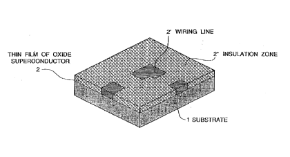
Figure 1 is an illustrative perspective view of superconducting
2 0 wiring lines provided by the first aspect of the present invention.
The superconducting wiring line 2' consists of at least a portion
of a crystalline thin film 2 made of oxide superconductor deposited on
a substrate 1. The superconducting wiring line 2' is made of a portion
of the thin film 2 whose an a-axis is oriented perpendicularly to a
surface of said substrate 1. The superconducting wiring line 2' is
surrounded by insulation zones 2" consisting of the ~ hlg portions
of the crystalline thin film 2 in which oxygen is removed out of the
crystals and hence they are changed to non-superconductor.
2 0 5 4 5 9 7
Example 2
Figure Figure 2A to 2H illustrate ~uccessi~c steps for fabricating
the superc~n~llcting wiring pattem shown in Figure 1.
In this example, at first, a substrate 1 having a smooth surface is
prepared (Fig. 2A). The substrate can be MgO (100) single crystal.
Other substrate such as CdNdA104 substrate or a silicon substrate having
a buffer layer can be used in place of the MgO single crystal.
Then, on the substrate 1, a thin film 2 of oxide ~u~ c~-~.du~lor
having a thickness of more than 200 nm is deposited (Fig. 2B). This thin
film 2 can be prepared by any technique including off-axis sputtering,
reactive evaporation or the like. In this Example, the thin film 2 of oxide
superconductor is prepared by the off-axis sputtering technique under the
presence of a mixed sputtering gas of Ar + ~2 (volume ratio of 9: 1) of
10 Pa. The substrate is heated at a temperature which is not higher than
650 ~C so that the thin film of oxide superconductor deposited becomes an
a-axis orientated thin filrn.
Then, as is shown in Figure 2C, an insulation layer or oxygen
barrier layer 3 is deposited. The oxygen barrier layer 3 may be made of
MgO, SiN, Au or the like.
Then, the oxygen barrier layer 3 is pattemed by known photo-
lithograph technique as is shown in Figure 2D. A pattem fommed in the
barrier layer 3 corresponds to the final superconducting wiring pattem.
In other words, the resulting patterned barrier layer 3a has the same
pattem as the superconducting wiring pattern.
2 5 The thin film of oxide superconductor 2 having the resulting
pattemed barrier layer 3a thereon is subjected to deoxygenation treatment
as is shown in Figure 2E. In this example, the deo~yg~ Lion is effected
by m~int~ining the substrate having the thin film of oxide ~u~ nd~
11
20 54 597
2 and the patterned barrier layer 3a thereon in a ultra-high vacuum
chamber for one hour while the substrate is heated at a le.llp~ ul~i which
is not higher than 400 ~C. During this deoxygenation treatment, oxygen
escape out of the thin film at the areas which are not covered with the
S barrier layer 3a to produce incllla~ing zones or non-~upe-c~\d-lctor zone
2a in the thin film 2 while the areas covered with the barrier layer 3a are
protected from the deoxygenation treatment to leave a patterned
supercnnducting wiring lines.
The resulting thin film having the patterned ~u~l-,on-lucting wiring
10 lines can be utilized as they are as a superconducting circuit having
conductor lines. In this case, an outer protective layer 4 is preferably
formed on a surface of the thin film 2 of oxide superconductor as is
shown in Figure 2F-1.
In a variation for fabricating a multi-layered superconducting
15 circuit having layered thin films of oxide superconductor, another upper
thin film layer of oxide superconductor is prepared by the steps shown in
Figure 2F-2 to 2H as following:
In this case, after the step of Figure 2E, a protective layer 4 is
deposited whole over the surface of the thin film 2 having the oxygen
2 0 barrier layer 3a as is shown in Figure 2F-2.
Then, the two layers of the protective layer 4 and the barrier layer
3a are etched back to leave a flat thin film layer 4' consisting of the
protective layer 4 and the barrier layer 3a as is shown inf Figure 2G.
When the flat thin film layer 4' is used as an interlayer barrier in a tunnel
2 5 type superconducting device utilizing the proximity effect, a thickness of
the flat thin film layer 4' must be reduced as thin as possible. This
etching can be carried out by a reactive ion etching tcrhniqn.~ or ion
milling te~hni~lue.
12
2 0 5 4 5 9 7
Finally, on a surface of the flat thin film layer 4', another thin film
S (Fig. 2H) of oxide ~upclcullJu~ tor in which an upper wiring pattem or
a suitable ~upel~onJ~Jcting element or device is r~b~ is dc~
The flat thin film layer 4' can be used as an insulator layer which
S separates adjacent two thin films layers 2 and 5 of oxide ~u~,~rco~lllu~ Jr
or can be used an il~t~ llayc;l barrier which functions as a weak junction in
a SII~ r~jng device utilizing the p-o~ y effect. In the latter case,
the thickness of the barrier layer 3a remained in the flat thin film layer 4'
must be as thin as possible. When the barrier layer 3a is made of an
10 insulator, the thickness of the barrier layer 3a remained is preferably
reduced to less than 10 nm so that a tunnel effect is realized by the barrier
layer 3a.
Example 3
Figure 3 is an illustrative perspective view of a superconducting
circuit provided by the second aspect of the present invention.
The superconducting circuit of Figure 3 has a thin film layer 2 of
oxide superconductor deposited on a substrate 1. The thin film layer 2 of
oxide superconductor comprises c-axis oriented thin film zones 21, a-axis
2 0 oriented thin film zones 22, insulation zones 23 in which
superconductivity is lost and viaholes 24.
The c-axis oriented thin film zones 21 provide superconducting
lines in which superconducting current is propagated in parallel with a
surface of the substrate 1. The a-axis oriented thin film zones 22 provide
2 5 superconducting lines in which superconducting current flow
perpendicularly to the surface of the substrate 1. No superconducting
current flow in the insulation zones 23. The viaholes 24 are used to
connect layers in a stacked multi-layered circuit (not shown).
13
-
2 0 5 4 5 9 7
Example 4
Figure 4A to 4F illustrate successive steps for fabricating the
supercon(luc~ing circuit shown in Figure 3. The oxide ~u~elco~ r
used in this Example 4 is a compound oxide superconductor of Y-Ba-Cu-
O system.
At first, a substrate 1 having a smooth surface is prepared. In this
Example 4, the substrate 1 consists of a silicon base substrate la having a
buffer layer Ib which is composed of an under-layer of MgA12O3 having
a thickness of 350 nm deposited by chemical vapour deposition (CVD)
technique and an upper-layer of BaTiO3 having a thickness of 75 nm
deposited by sputtering technique. MgO (100) substrate, CdNdAI04
substrate or the like can be preferably used in place of the silicon
substrate. On the buffer layer I b of the substrate 1, a thin film 2 of oxide
superconductor having a thickness of more than 200 nm as is shown in
Figure 4B is deposited. This thin film 2 can be prepared by an off-axis
sputtering technique, a reactive evaporation technique the like. In this
Example 4, the thin film 2 of oxide superconductor is prepared by the
off-axis sputtering technique under the presence of a mixed sputtering gas
of Ar + ~2 (volume ratio of 9: 1) of 10 Pa. The substrate is heated at a
2 0 L~ eldlul~ above 700 ~C so that the thin film of oxide superconductor
deposited shows c-axis orientation.
Then, as is shown in Figure 4C, a photoresist layer 3 having a
predetermined patter is coated on the thin film 2 of oxide superconductor
obtained by a well-known technique.
2 5 After the photoresist layer 3 is cured, exposed areas which are not
covered with the photoresist 3 are removed by a dry etching technique
such as reactive ion etching and argon milling or by a wet etching
te~ ue such as treatment with phosphoric acid or hydrochloric acid, so
14
2054 597
as to produce a pattemed superc~n~lucting lines 2c concic~ing of the c-axis
oriented thin film as is shown in Figure 4D.
Then, as is shown in Fig. 4E, an a-axis oriented thin film 2a of the
same oxide superconductor is deposited on the surface of the substrate l
S having the patterned superconducting lines 2c concicting of the c-axis
oriented thin film. This thin film 2a of oxide superconductor also is
prepared by the off-axis sputtering technique under the presence of a
mixed sputtering gas of Ar + ~2 (volume ratio of 9: l) of lO Pa but the
substrate is heated at a temperature which is not higher than 650 ~C so
l 0 that the thin film of oxide superconductor 2a deposited becomes an a-axis
oriented thin film.
After then, a surface of the a-axis oriented thin film 2a is smoothed
by a dry etching technique such as reactive ion etching or argon milling to
obtain a superconducting circuit according to the present invention as is
l 5 shown in Figure 4F in which both of the superconducting lines 2c made of
c-axis oriented thin filrn and the superconducting lines 2a made of a-axis
oriented thin film make a planar surface on a common plane or on the
surface of the substrate l.
In practice, an insulator layer may be deposited on a surface of the
2 0 resulting superconducting circuit of Figure 3 before the circuit is passed
to next stage for completing the superconducting circuit into a desired
superconducting device.
The insulation zones 23 shown in Figure 3 can be prepared by
deoxygenation of the thin film 2 of oxide superconductor. Namely, after
2s predetermined areas of the thin film 2 of oxide superconductor are
protected with photoresist or insulator, remaining exposed areas are
subjected to a treatment of deoxygenation so that the exposed areas are
changed into non-superconductor.