Note: Descriptions are shown in the official language in which they were submitted.
2~5~6~4
SPECIFICATION
Title of the Invention
SUPERCO~DUCTlNG DE~e~ HAVING AN EXT~EMELY
SHORT SUPERCONDUCI'ING CHANNEL FORMBD OP
EXTREMELY THIN OXlDE SUPERCONDUCTOR FLM AND
METHOD FOR MANUPACI'URING THE SAME
Background of the Invention
~ield of the invention
The present invention relates to a suye.conducting device and a
method for manufactur;ng the same, and more specifically to a
superconducting device inc]uding an extreme]y thin ~uyel~onducting
channel formed of oxide superconductor materia], and a method for
manufactnnn~ the same.
Description of related art
Typical devices utilizing a superconductor include a so called
Josephson device, which c~ ylises a pair of supcrco~ductors coupled to
each other through a tunnel barrier. The Josephson device can realize a
high speed swilchillg. However, the Josephson device is a two-terminal
device, and therefore, requires a complicated circuit in order to reali~ a
logic circuit.
On the other hand, typical three-terminal devices utilizing a
ye~onductor include a so called su~e~co~ ctin~-ba~se transistor and a
so called super-FET (field effect transislor). The suyer~;onclllct~ base
transistor includes an emitter of a supercontlllctor or a normal conductor,
: - , ,.. ,: .
, . - ~. .
- .
.. ~
. - . . .. ... . . .. .
:. ..
;.
..
44
a tunnel barrier of an insulator, a base of a superconductor, a
semiconductor isolator and a collector of a normal conductor, s~acked in
~e named order. lllis sup- rcol~dl~ctin~-base transistor Ope~alCS at a high
speed with a low power collsul~plion, by utili7ing high speed electrons
passing through the tunnel barrier.
The super-FET includes a semiconductor layer, and a
su~;,conductor source electrode and a superconductor drain electrode
which are formed closely to each other on the semiconductor layer. A
portion of the semiconductor layer between the s~perconductor source
electrode and the superconductor drain electrode has a gready recessed or
undercut rear surface so as to have a reduced thickness. In addition, a
gate electrode is formed through a gate insulating layer on the recessed or
undercut rear surface of the portion of the semiconductor layer ~etwee
the suyerconductor source electrode and the superconductor drain
electrode.
A superconducting current flowing through the semiconductor
layer portion b~lwe~ll lhe superconductor source electrode and the
~u~reol-ductor drain electrode due to a su~elcondl~ctin~ proximity effect,
is controlled by an applied gate voltage. This super-FET also ope~ s at
a high speed with a low power con.c~u~llt;on.
In addition, in the prior art, there has been proposed a
three-terrninal superconducting device having a channel of a
~ ,e-collductor formed between a source electrode and a drain electrode,
so that a current flowing through the superconducting channel is
control~ed by a voltage applied to a gate formed above the
s~ ;ol.-lucting channel.
,
~: . . . -
..
. ~....... .
2(~S44
Both of the above mentioned ~u~)erconducting-base transistor and
the super-FET have a portion in which a semiconductor layer and a
SU~eI~;O~dU~ layer are stacked to each other. HoweYer, it is difficult
to form a staclced structure of tbe semiconductor layer and the
sul,e.eollducting layer formed of an oxide ~uperconductor which has
recently advanced in study. In addition, even if it is possible to fonn a
stacked structure of the semiconductor layer and the oxide
su~)e~conducting layer, it is difficult to control a boundaly bel..eel~ the
semicon~1uctot layer and the oxide ~u~erco~ cting layer. Therefore, a
y operation could not been obtained in these ~ e~ollducting
devices.
In additiorl, since the super-FET utilizes the superconducting
proximity effect, the superconductor source electrode and the
~ulJe~onductor drain electrode have to be located close to each other at a
I;sl; nce which is not greater than a few times the coherence length of the
~upwconductor materials of the su~c~.iQn~ cto~ source electrode and the
superconductor drain electrode. ~n particular, since an oxide
ol-rluctQr has a short coherence length, if the supercol~ ctor source
electrode and the superconductor drain electrode are formed of the oxide
sup~c~nductor material, a distance between the supe~on(luctor source
electrode and the superconductor drain electrode has to be not greater
than a few ten nanometers. However~ it is very dif~lcult to conduct a fine
processing such as a fine pattern etching so as to ensure the very short
separation distance. Because of this, in the prior art, it has been
impossible to manufacture the super-FET composed of the oxide
clcor..luctor material with good reproducibility.
.. . . . . .. ..
, '. ~' ' , ' '' ' ,~',' - ' ' ''
,~ '. ~ ' '
.: . ' -, :.
ZC~44
Furthermore, it has been confirmed that the conventional
three-terminal superconducting device having the superconducting
channel shows a modulation operation. However, the conventional
three-terminal superconducting device having the superconducting
channel could not realize a complete ON/OFF operation, because a carrier
density is too high. In this connection, since an oxide &u~erconductor
material has a low carrier density, it is e~lrecred to forrn a lhree-tenninal
efeollducting device which has a ~uperconducting channel and which
can realize the complete ONlOFF operation, by forming the
~u~lco~lducting channel of the oxide superconductor material, In thi~
case, however, a thickne~ Df the ~upL.~;ollducting channel has to be made
on ~e oreler of five nanometers. This extremely thin superconducting
chaDnel is difficult to realize.
On the other hand, in order to realize a high speed ONtOFF
operation in the above mentioned sul,erconducting device, it is nececs~ry
to shorten a gate length. In order to shorten the gate length, the gate
electrode has to have a shape which is short in a direction of a current
nowing through the superconducting channel, for example, not greater
than 100nm. It is practic~lly very difficult to form the gate e1ectrode
having the above men~ioned size on the oxide su~erconductor by a
conventional fine~working (fine-etching) technique with good
reproducibility .
Somm~ly 0~ the lnvention
Accordingly, it is an object of the present invention to provide a
c~onducting device and a method for manufacturing the same, which
havè overcome the above mentioned defects of the co--vel,tional ones.
: - , -.
- . . : .- ,. . ::.
,
. ~, . ::
Z~5
Another object of the present invention is to provide a
~upe,-,onducting device including a ~up~l~'onductin~ re~ion conDIi~uled of
an eAII.,.llely thin oxide super~onductor film, which can be manufactured
by using existing established processing techniques with a good
repeatability.
Still another object of the present invention is to provide an FET
type superconducting device including an extremely short
~u~e~col-dllcting channel composed of an oxide supcleonductor thin fflm,
and a method for manufacturing the same with a good repeatability by
using existing established ~lu~e~s;ng te~ ,f,s.
The above and olher objects of the present invention are achieved in
accordance with the present invention by a superconducting device
ec)~ isillg a substrate, a su~,ercol-ductin~ channel constituted in an oxide
supercon~ ctor thin film deposited on a deposition surface of the
substrate, a source electrode and a drain electrode formed on the oxide
s.,pc~col--lu~ lor thin fi~m at ol)pGsilc ends of the ;,up~ on~Ucting eh~nnel,
so that a ~u~crconducting current can flow through the su~rconducting
channel between the superconductor source electrode and the
~u~,.col~ductor drain electrode, and a gate electrode formed through a
gate insulator layer on the supereonducting channel so as to control the
~u~e..;onducting current flowing through the supercoud~ ting channel,
the Bate electrode being in the fonn of a thin film standing upright to the
gate insulator layer.
In one en~bodimen~ the ~u~ef~ionducting channel has a thickness of
not greater than ~lve n~nonlrt~rs, and the oxide su~ercol-ductQr thin film
has an upper planar surface. The gate lnc.ll~or layer is deposited on the
upper planar surface of the oxide superconductor thin film, and an
.. .. , . -. ~, ..
. .
.' . , ~- ' ,~ - ., ''
~ .~ , -- - ~ .
- . ' ~, . ' - ' ' ! ' '
ZC'5~5~44
insulating protec~ion layer is forrned on the gate insulator layer and
having an end surface angled to the gate insulator layer. The gate
electrode is fonned of a thin film of a normal con~l-ctor deposited on the
end surface of the in~ ting protection layer.
The above mentioned superconducting device can be formed in
accordance with a method of the present invention, by forming on- a
substrate an oxide ~u~crec~ ctor thin film having a planar upper surface
and a ~u~)e..io~-ducting region having a thiclrness of not greater than five
nanometers, de~Gsi~ g a gate insulator layer on the planar upper surface
of the oxide su~erconductor thin film, forming a plurality of insulating
protection layers on the gate insulator layer in such a manner that a
selected one of the insnlating protection layers has an end surface
positioned above the ~u~crc.".~uctine region having the thickness of not
greater than five n~nnmeters~ and forming a gate electrode in the forrn of
a th;n film on the end surface ~f the selected insu]ating protection layer.
In another embodiment, the gate electrode being in the fo~m of a
thin film is embedded in the substrate. This gate electrode in the forrn of
a thin film and embedded in the substrate can be formed by de~)osiling an
oxide ~u~,er.io"ductor thin film on an ins~ n~ substrate having a stepped
portion or a semiconductor substrate having a stepped pordon and coated
with an insulating layer, selectively removing the deposited oxide
~u~-co~lductor thin film from the substrate so as to leave the deposited
oxide superconductor thin film on only the side surface of the stepped
portion, and filling a material (for exarnple, the same rnateria~ as that of
the substrate) into a recess formed by the stepped portion.
In still another embodiment, the gate electrode being in the form of
a thin film is located on the substrate, and the source ~1PI t~od~ anLthe
. . - .
Z(~ 544
drain.electrode are formed of an oxide superconducting source electtode
and an oxide sul~e-conducting drain electrode, respectively, which are
located on the oxide supelconductor thin film of the superconducting
channel through an extremely thin insulator layer. E~loccul~tion occurs in
the extremely thin insulator layer sandwiched between the o~ide
supel~condnctQr thin film of the supercon~1ucting channel and each of the
oxide ~u~ercol-ducting source electrode and the oxide su~?crconducting
drain electrode, so that the superconducting source electrode and the
s~,perco~ducting drain electrode are in electrical connection with the
o~ide sul)ereonductor thin film of the superconducting channel.
In this embodiment, the oxide superconductor thin film of the
superconducting channel is formed of a c-axis oriented oxide
superconductor crystal layer formed on the substrate, and the
su~)e~co~ducting snurce electrode, the supercon(l~lcting gate electrode and
the superconducting drain electrode are formed of an a-axis oriented
oxide ~el.;on~ ctor crystal layer folTned on the extsemely thin insulator
layer.
As seen from the above, the sllpe-conducting device in accordance
with the present invention includes the ~u~c~conducting channel formed of
the oxide ~u~erconductor thin film, the source electrode and the drain
electrode for causing a current to flow through the supercondl-cting
channel, and the gate electrode for controlling the current flowing
~rough the ~ul,eJLonducting channel. Here, each of the three electrodes
must be not n~ce~c~rily consli~uted of a s.,l,~,.co,~ducting electrode.
As mentioned above, in the superconducting device iD accordance
with the present invention, the ;,tl~c~ol-ducting channel is col-c~ d of a
portion of the oxide superconductor thin film having the planar upper
;. . - . .: . - ' .
..
- i -. . -,.. ",
-: .
Z~ 544
surface. In order to turn on and off the gate (namely, the
superconducting channel) by a voltage applied to the gate electrode, the
thickness of the superconducting channel in a direction of an electric field
created by the gate electrode must be not greater than five nanometers.
Such an extremely thin oxide supe-~o!ldllctor thin film can be formed in a
conventional process by precisely controlling the grQwth speed and the
growth time of the thin film. For this purpose, a s~ull~ g can be used.
However, since the oxide superconductor crystal has a multi-layer
~llucLul~ in which ~ ,eclive constituent elements are stacked in a layered
structure, it is possible to stack a desired number of unit ce]ls of oxide
s. pelco~ ctor, by using a MBE (molecular beam epita~y).
In the supercondllcting channel-FET having a channel formed of an
oxide superconductor thin film, only a portion of the oxide
supe~ondllctor thin film subjected to an electric field given by an applied
gate vo}tage can flow and block an electric current. Therefore, the
channel length is substantially determined by the gate length of the gate
electrode. The gate length is a length of the gate electrode in a direction
of a current flowing through the superconducting channel. Namely, in
the ~.,pelconducting device in acc~,ld~l-ce with the present invention, since
the extremely thin gate electrode stands upright on the s~l)e~onducting
channel through the gate insulator layer, the gate length of the gate
electrode is subst~nti~lly determined by the thickness of the oxide
superconductor thin film of the gate electrode. Preferably, the gate
electrode has a thickness of not grea~er than lOOnm. ln any case, thinner
the gate electrode (in the form of a thin film) becomes, the shorter the
gate length becomes. Accordingly, in the ~ e~conducting device in
accordance with the present invention, an extremely short gate length and
.
- .: . . . . .. .. . .
2C'~;44
hence a corresponding extremely short superconducting channel can be
realized by this extremely thin gate electrode, so that the ON/OFF
operation can be speeded up.
As mentioned above, only the portion of the oxide ~u~el.;onductor
thin film superconducting channel layer subjected to an electric field
given by an applied gate voltage con.~tit ~tes the ~u~lconducting channel
which can flow and block an electric cutrent. Namely, the other portion
nf the nxide ~ur1ercnnductm ~hin film ~uperconduc~ing çh~nnel l~yer does
not contribute ON/OFF of the current, and the.efole, it can be understood
that, a portion of the oxide superconductor thin film ~u~)e,~;onducting
channel layer that does not contribute ON/OFF of the current, is a portion
of a source electrode or a drain electrode. In this specification, ll,e,erurb,
the source electrode should be understood to include not only an electrode
co.l~,i",ollding to the electrode which is called a "source electrode" in the
field of a semiconductor MOSFET, but al~so a source region which is
formed ~ljac~n1 to and continuous to the s..pe.~onducting channel and on
which the source electrode is formed, and the drain electrode should be
llnde,~ood to include nol only an electrode corresponding to the electrode
which is called a "drAin electrode" in the field of the semiconductor
MOSFET, but also a drain region which is formed adjacent to and
continuous to the su?erconducting channel and on which the drain
electrode is fotmed~
As m~ntisn~d above, the thin film of the gate electrode is provided
on the end surface of the insul~ting protection layer. Therefore, it is
possible to easily forrn the thin film of the gate electrode on the end
surface of the insulating protection layer, by depositing a conductive
ma~erial onto the end surface of the insulating protection layet.
-- ..
- ~
- .
: ~- -
. ~ .
Z~5~5AA
Accordin~,ly, the superconducting device in accordance with the present
invention can have the above m P.n~iQIl~.d shortened gate without using the
fine-processing tPçhnique~
In ~he superconducting device in accordance with the present
invention, the above mentioned extremely thin su~clco~ rting channel is
reali~ed as follows:
(1) Components of the substrate are selectively diffused into the oxide
superconductor layer deposited on the substrate, so that a
non-~up~.co~ cting region is forrned in the oxide supelconductor thin
film. The non-superconducting region thus formed in the oxide
superconduct~r thin film acts to thin a superconducting portion of the
oxide su~)elcollductor thin film.
(2) A projection is previously formed on the substrate, and an oxide
~u~ conductor thin film having a planar upper surface is forrned to
cover dle projection of the substrate. As a rcsult, an extremely thin
portion of the oxide superconductor thin film is formed above the
projection of the substrate.
~ n the forrner case, constituent element(s) of the substrate can be
diffused into the oxide superconductor thin film. Otherwise, a portion of
d~e substrate surface can be previously provided with a layer or island of
a material which diffuses into an oxide ~upe~ol~uctQr thin filrn in the
course of the deposition of the oxide superconductor thin film so as to
destroy superconductivity in a diffused portion of the deposited oxide
elconductor thin film. In order to cause the constituent element(s) of
the substrate to diffuse into the oxide supercrndllc~or thin film, energy is
locally applied to a position of the oxide su~,en;onductor thin film where
~e sup~ ;onducting channel is to be for~med, by a focused ion beam, a
- 10-
,.. . .
. ~ . . . ......... . .
.. - . . ..
2~544
laser, or the like, so that the constituent element(s) of a substrate portion
under the superconducting channel forming position of the oxide
superconductor thin film is c~used to diffuse into the oxide
ond.~clor thin film.
In general, the oxide superconductor has large crystalline
inhomogeneity. In particular, the critical current density is larger in
direc~ions ~n~ c~ r to the c-axis, ~an in a direction paTallel to the
c-axis. Therefore, if a superconducting source electrode and a
supelconducting drain electrode have been formed of c-axis oriented
oxide superconductor thin films, it has been difficult to cause a
;,.,pe.Lollducting current to uniformly flow through an extremely thin
erconducting channel of an oxide sllpcrconductor. As mentioned
above, in the superconducting device in accordance with the present
invention, sillce the superconducting source electrode and the
supe~ondueting drain electrode are formed of an a-axis oriented oxide
su~erc~ ctor thin film, the main current is allowed to flow within the
~u~e.cu~ducdng source electrode and the supe-conducting drain electrode
in a direction perpendicu]ar to the substr~. On the other hand, since the
superconducting channel is formed of a c-axis oriented oxide
~u~c~r.~h.~tor thin film, the m~in current i5 allowed t~ flow within thc
~u~c~onducting channel in a direction parallel to the substrate.
Therefore, in each of the superconducting source electrode, the
~erconducting drain electrode and the su~,elconducting channel, the
main current is caused to flow in a direction having a large critical
current density of the oxide sul~erconductor crystal.
The c-axis oriented oxide supefconductor thin film sup~nconducting
channel can be easily formed by maintaining the substrate at a
'
,. : ; '- ".:
- . .
Z~ 44
al,plopliate buffer layer is deposi~d thereon. For example, the buffer
layer on the semiconductor substrate can be formed of a double-layer
coating fonned of a MgAl204 layer and a BaTiO3 layer, or a single ]ayer
of "YSZ" (yttrium stabilized zirconia) or Y203 if a silicon substrate is
used.
The above and other objects, features and advantages of the present
invention will ~e al",a,~,nl from the following description of p.e~e"ed
emb~dimPnt~ of the invention with reference to the accon~)allying
drawings.
Brief Description of the Drawings
Figures lA and lB are diagrammatic sectional views of
embodiment~ of the superconducting device in accordance with the
precsnt invontion;
Figure 2A to 2G are diagrammatic sectional views illustrating an
emboclim~.n~ of the process for n~ fa~~uring the ~u~c,~ionducting devices
shown in Figure I A and IB;
Figure 3A to 3K are diagram-natic sectional views illustrating an
P-~bodi~--f~ of the process for m~nnfactllring a second embodiment of the
su~ c)n~h~eting device in accordallce with the present invention; and
Figure 4A to 4L are dia~.n.. ~tic sectional views illu~ .ling an
~...ho~ of the process for m~n-lfacturing a third embodiment of the
s.-pe.c~ cting device in accorddnu with the present invention.
- 13-
- . . .: . - . .
... ~... ......
Z~ i44
Description of the Preferred embodiments
Embodiment 1
Referring to Figures lA and lB, there are shown diagrammatic
section~l views of two embodiments of the superconducting devices in
r-:Dr~anCe with the present mvention. In these Figures, çl~m~.ntc similar
to each other are given the same Rercl~,nce Numerals.
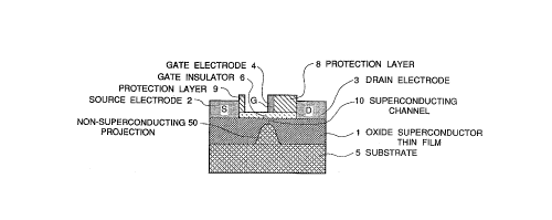
The ~u?e~o~ducting device shown in Figure 1 includes an oxide
superconductor thin film 1 formed on a substrate 5 and having a
non-superconductin~ region 50 which is formed by diffusion of
coll~tituer t element(s) into the oxide ;iu~ eul-ductor thin film and which
no longer has su~erconductivity. The oxide su~ uctor thin film
fonns a superconducting channel 10 of about five nanometers in ~hir~nP.~
at a position above the non-superconducting region 50. On the
superconducting channel 10, an extremely thin gate electrode 4 is
provided through a ~ate insulator layer 6. A source electrode 2 and a
drain electrode 3 are located on the oxide superconductor thin film I at
opposite sides of the ~ o~ lcting channel 10, respectively.
The gate eleclrode 4 is fonned of a normal conductor thin film or
an oxide ~ c.col~J~Ictor thin film, and is deposited on a side surface of a
surface p~ etion layer 8 formed on the gate jn~llkttûr 6. The normal
c~n~nctor thin film can be deposited on the side surface of the su~ace
p~uleclioll layer 8 by for example an inclinpd evaporation process. The
oxide ~u~ J Ictor thin film can be deposited on the side surface of the
surface protection layer 8 by for example an off-axis s~ut~ g. As seen
from the drawing, the thin film of the gate electrode 4 stands upright on
the gate insltl~or, and therefore, the thiel~n~ss of the thin film of the gate
electrode 4 det~ es a gate length.
- 14-
.
',
~ ' ,'., ' . ~' ' ,
~ . ., '' ' ~ ',','', " ." '' '; ', ~"'" '' '. ' '' ' " '
''. ' . .'' " I '
Z~ 4A
The embodiment shown in Figure I B is different from the
embodiment shown in Figure lA, only in that the non-superconducting
re~ion 50 is con~titut~d of a projection previously fo~ned on the substrate
5. The other features of tlle embodiment shown in Figure IB are
completely dle same as those of the embodiment shown in Figure ~ A, and
ererc,.~, further e~pl~n~t;on will be omitted.
Now, a process for manufacturing the superconducting device
shown in Figure lA will be described with reference to Figures 2A to 2G.
First, a substrate 5 is prepared as shown in Figure 2A, This
substrate 5 is formed of for example, an insulating substrate such as a
MgO (100) substrate, a SrTiO3 (I00~ substrate or others, or a
semiconductor substrate such as a silicon (100) substrate having a
p,il~ei~Jal surface coated with insulating films. However, if the silicon
substrate is used, a principal surface of the silicon substrate is
continuously coated wi~h MgAI2O4 by a CVD process and with BaTiO3
by a Sp~ g process.
Then, as shown in Figure 2B, an oxide su~ercul-ductQr thin fi]m 1
having a thickness on the order of 200nm to 300nm i9 deposited on the
~uL,Ilat~ 5, by for example an off-axis sputtering, a reactive evaporation,
an MBE (molecular beam epitaxy), a CVD, etc. The oxide
s,lpclconductor material is preferably formed of, for example, a
Y-Ba-Cu-O type compound oxide superconductor materia], a
Bi-Sr-Ca-Cu-O type conlpuulld oxide superconductor material, and a
Tl-Ba-Ca-Cu-O type compound oxide superconductor material. The
oxide ~.lp~ nductor thin fi]m is preferably formed of a c-axis orientated
oxide ~ elcollductor thin film, since the c-axis orientated oxide
rconductor thin film has a large cri~ical current density in a direction
.. . . .
- ; . --,, ' , .: . ' '~
., .. :: ~ -: : : ; '
2~ ~S44
parallel to the substrate. The c-axis orientated oxide sul~elcollductor thin
film can be formed by m~in~Aining ~e substrate temperature at about
700~C in a filtn deposition process.
Next, a laser beam or a focused ion beam is locally irradiated onto
~e ~xide ~u~e.~onductor thin film l, as shown by arrows in Figure 2C,
so that cc~nntituent ele~ .l(s) of the substrate 5 is caused to diffuse into
the oxide superconductor thin film 1 so as to form the
non ~.lpe,co~ ,cting region 50. A portion of the oxide superconductor
thin film rem~ining above the non-superconducting region 50 forms the
ducting chasmel lO.
In the case of forming the non-superconducting region 50 by
irradiating the laser beam, it is preferable to use a hi~h power laser beam
such as an excimer laser, a CO2 laser, a YAG laser, etc. For example,
when an Ar laser having a waveleng~h of 514nm is used, it is preferred to
scan the laser beam having an irradiation output power of 2.0W at a speed
of lOOIlm/second. On the other hand, in d~e case of forming the
non superc~-n~ cting region 50 by irradiating the focused ion beam, it iS
plcr~ ed to irradiate Ar ions with a beam diameter of not greater than
O.~m and an acceleration voltage of not greater than SOKV.
Here, the process shown in Figures 2B and 2C can be replaced by a
process illustrated in Figures 2BB and 2CC.
Namely, as shown in Figure 2BB, an focused ion beam is locally
irradiated onto the substrate S so as to form a doped region 51. Thc
irradiated ions preferably are Ba ions, Y ions, or Cu ions. In addition, it
is also ~-~fel~d that the beam di~meter is 0.211m and the acceleration
voltage is ~OKV. The doped region S l having a wid~ of not greater than
- 16-
.
,; ':'':' . :
~ .~ . . ,. . - :: .
. . .
X~ i4~
Illm is formed on the principal surface of the substrate 5 by irradiation of
the focused ion beam.
The.~afle~, as shown in Pigure 2CC, ~e oxide superconductor thin
film 1 is deposited on the substrate 5 having the doped region 51, by for
e~mrlP the off-axis s~ e.h~g, the reactive evaporation, the MBE, the
CVD, etc., similarly to the process of Figure 2C. In the process of
growth of the oxide s,lyel~ionductor thin film 1 on the substrate 5, doped
elements are diffused from the doped region 51 into the oxide
su~,cl~ion~l~)ctQr thin film 1 so as to form the non-superconductin~ region
50. A superconducting portion of the oxide superconductor thin film
remaining above the non-superconducting region 50 forms the
~up~rconducting channel 10.
Th~.edfler, as shown in Pigure 2D, an insulator film 16 is formed
on the oxide superconductor thin film l, and then, surface protection
inSu~ ng layers 8 and 9 are forrned on the insulator film ~ 6, excluding a
limited region above the supercnr~ cting channel 10. The in~ul~ting
layer 16 is preferably fonned of an in~ til-g material such as MgO,
which does not form a large density of energy levels beL.._en the
~u~ ol-d11ctor thin film I and the insulating layer 16. In addition, the
insulating layer 16 has a thickness sufflcient to prevent a tunnel current,
for example, a thickness of not less than 10 nanometers. The surface
protection in~ ing layers 8 and 9 are preferably formed of MgO.
As shown in Figure 2E~, a normal conductor ~llm 1~ is formed on
the surface protection layer 8 by ~e,S~ ing an evaporation in an inclined
direction so as to ensure that the normal conductor film ~ 8 is deposiL~d on
a side surface 8A of the surface protection layer 8 positioned above the
s,l~,cl.o~d~1ct;n~ channel 10. In this process, another norrnal conJu-ilor
- 17-
. . .
- : , . -
.. ~ : .,
ZC'5~544
film 19 is simultaneously formed on the surface protection layer 9.However, this nonnal conductor film 19 is not necei~ar~ These normal
conductor films 18 and 19 are preferably formed of a refractory metal
such as Ti, W, etc., or Au, or a silicide thereof.
Then, as shown in Figure 2F, an anisotropic etching i6 conducted on
the nonnal conductor films 18 and 19 by means of a reactive ion etching,
or an Ar-ion milling, so that a portion of ~e norrnal con~1uctor film 18
remains only on the side surface 8A of of the surface protection layer 8.
This rl~m~inin~ nonnal condl~ctor film 18 forrns a gate electrode 4. This
gate electrode 4 is preferred to have a thickness of not greater than
100nm.
Finallyl as shown in Figure 2G, the insulator film 16 and ~e
surface protection layers 8 and 9 are removed from opposite end regions
of the oxide s.lpelcol7ductor thin ~llm 1. Th~ fore, the insulator film 16
re~qining above the supercond~lcting channel 10 forms a gate insulator
layer 6. On the other hand~ a source electro~e 2 and a drain electrode 3
are formed on the opposite exposed end regions of the oxide
su~erconductor thin film 1. The source electrode 2 and the drain
electrode 3 are formed of the same normal conductor material as that of
the gate electrode. Thus, the su~elc~ ductillg channel-~:ET is completed.
In the above mentioned embodiment, the non-sul,el.ioll.lucting
region S0 is forrned by diffusing the constituent element(s) of the
subsnate into the oxide s-lp~lco~ nctc-r thin film ~ . The present invention
is not limited to this method. For example, in the case of m~n~r~ct~ g
the i~u~,rconducting device as shown in Figure lB, the substrate is
previously machin.~t? or etched so as to have a projection co~sponding to
~e non-sul~erco.-ducting region 50, and then, the oxide s,.~e.collductor
- 18-
- . ~ ~ . .~, - . -, .
.. .. ; . . . :,. :,.. . . .
..
- - : . . ... i., ,,, ~ , . .
CA 02054644 1997-11-18
thin film 1 is deposited on the substrate surfaoe having the projection, and
thereafter, is planarized so that the oxide superconductor thin filrn 1 has
an flat upper surface.
In the above mentioned embo-liment, the gate electrode is formed of
a norrnal conductor, but can be formed of an oxide superconductor. In
the latter case, after the insular film 16 is formed, an oxide
sll~r.;o,lductor thin film which has a thickness of not greater than 100nm
and which is preferably an a-axis oriented film, is deposited, and then, the
Ar-ion milling and the anisotropic etching are performed in an inclined
direction so as to shape a superconducting gate electrode. Thereafter, the
protection layers 8 and 9 are formed.
Embodiment 2
Referring to Figure 3K, there are shown diagr~mm~tic sectional
views of a second embodiment of the superconducting device in
accordance with the present invention. In Figure 3K, elements similar to
those shown in Figures lA to 2G are given the same Refen~nce Numerals.
The superconducting device shown in Figure 3K includes a gate
insulator layer 6 and an oxide superconductor thin film 1 forrned in the
named order on a substrate S having a superconducting gate electrode 4
embedded therein. A surface protection layer 7 is formed on a portion
of the oxide superconductor thin film 1 above the superconducting gate
electrode 4. A source electrode 2 and a drain electrode 3 are formed on
the oxide superconductor thin film 1 at both sides of the surface
protection layer 7, respectively.
The oxide superconductor thin film 1 is formed of a c-axis oriented
oxide superconductor crystal layer having a thickness of not greater than
- 19-
CA 02054644 1997~ 18
about five nanometers, so that a portion of the oxide superconductor ~in
film 1 above the elTbedded supercon~lctin~ gate electrode 4 folms the
superconducting channel 10. The gate in~ul~tor layer 6 is l .~fcl~bly
formed of an insulating material such as MgO, Si3N4, and has a ~hic~ness
sufficient to prevent a tunnel current, for example, a ~ickness of not less
than 10 nanometers. The superconducting gate electrode 4 is formed of
an a-axis oriented oxide superconductor crystal layer and has a thi~n~ss
of not greater than about 100nm in a direction of an electric current
flowing through the superconducting channel 10.
Now, a process for manufacturing the superconducting device
shown in Figure 3K will be described with reference to Figures 3A to 3K.
First, a substrate 5 is prepared as shown in Figure 3A. Similarly to
the first embodiment, this substrate 5 is formed of for example, an
insulating substrate such as a MgO (100) substrate, a SrTiO3 (100)
substrate or others, or a semiconductor substrate such as a silicon (100)
substrate having a principal surface coated with an insulating film.
However, if the silicon substrate is used, the silicon substrate is coated
with an insulating filrn after a step explained hereinafter is formed.
As shown in Figure 3B, a photoresist 20 is deposited and patterned
to cover a portion 5A of the substrate, and then, an uncovered portion of
the substrate S is etched by a dry etching such as a reactive ion etching
and an Ar-ion milling, so that a step 53 is formed as shown in Figure 3C.
Thereafter, the photoresist 20 is removed.
In the case that a semiconductor substrate is used, a crystalline
direction is important, and therefore, the process is modified. For
example, if a silicon substrate is used, a photoresist mask 20 is formed so
as to ensure that a gate length direction (a channel current direction) is
- 20 -
CA 020S4644 1997~ 18
perpendicular to a Si(l lO) plane. The silicon substrate partially masked
with the photoresist 20 is etched with an etching liquid such as KOH or
APW, so that a step 53 is formed as shown in Figure 3C. After the
photoresist mask 20 is removed, the principal surface having the step 53 is
contil-uously coated with MgA104 by a CVD (chemical vapor deposition)
and with BaTiO3 by a sputtering process.
Then, as shown in Figure 3D, an a-axis oxide superconductor ~in
film 11 having a thickness of not greater than lOOnm is deposited on the
principal surface of the substrate 5 at a substrate temperature of not
greater than 650~C, by for example an off-axis sputtering, a reactive
evaporation, an MBE (molecular beam epitaxy), a CVD, etc. The oxide
superconductor material is preferably forrned of, for example, a
Y-Ba-Cu-O type compound oxide superconductor material, a
Bi-Sr-Ca-Cu-O type compound oxide superconductor material, and a
Tl-Ba-Ca-Cu-O type compound oxide superconductor material. The a-
axis orientated thin film has a large critical current density in a direction
perpendicular to the substrate surface.
The oxide superconductor thin film l l is selectively removed from
a projected portion 5A and a recessed portion SB of the substrate surface
by an anisotropic etching such as a reactive ion etching, so that a
superconducting gate electrode 4 is formed on only a side surface of the
step 53 as shown in Figure 3E.
The same material as that of the substrate 5 is deposited by
sputtering so that a layer 54 having a thickness sufficient to perfectly fill
the recessed portion SB, as shown in Figure 3F. In addition, a photoresist
(not shown) is deposited to cover the layer 54 and to have a flat upper
surface. Thereafter, as shown in Figure 3G, the photoresist on the layer
- 21 -
CA 02054644 1997-11-18
50 and the layer 50 itself are etched backed and planarized by the Ar-ion
~tc-hin~ until an upper end of the superconducting gate electrode 4 is
exposed.
As shown in Figure 3H, a gate insulator layer 6 is formed on the
planarized surface of the substrate 5. This gate insulator layer 6 is
preferably formed of an insulating material such as MgO, which does not
form a large density of energy levels between the oxide su~,erco,lductor
thin film and the gate insulator layer 6. In addition, the gate insulator
layer 6 has a thickness sufficient to prevent a tunnel current, for example,
a thickness of not less than 10 nanometers.
As shown in Figure 3I, a c-axis oxide superconductor thin film 1
having a thickness of not greater than five nanometers is deposited on the
gate insulator layer 6. This c-axis oxide superconductor thin film 1 can
be formed at a substrate temperature of about 700~C, by for example an
off-a~is sputtering, a reactive evaporation, the MBE, the CVD, etc. The
c-axis orientated thin film has a large critical current density in a
direction in parallel to the substrate surface.
As shown in Figure 3J, a surface protection layer 17 is deposited to
cover the whole of the oxide superconductor thin film 1. Thereafter, dle
surface protection layer 17 is selectively removed so that the surface
protection layer 17 remains only above the superconducting gate electrode
4. A source electrode 2 and a drain electrode 3 are forrned on the oxide
superconductor thin film 1 at both ~ide~ of the remaining surface
protection layer 7. The source electrode 2 and the drain electrode 3 are
formed of a no~nal conductor, for example, a refractory metal such as
Ti, W, etc., or Au, or a silicide thereof, or an oxide superconducting
material.
CA 020S4644 1997~ 18
Embodiment 3
Referring to Figure 4L, there are shown diagrammatic sectional
views of a third embodiment of the superconducting device in acc~r~auce
with the present invention. In Figure 4L, element~ similar to those shown
in Figures lA to 3K are given the same Reference Numerals. -
The superconducting device shown in ~igure 4L includes an oxide
superconductor thin film 1 deposited on a substrate 5 so as to form a
superconducting channel. An insulating layer 61 is formed on dle oxide
superconductor thin film 1 above the superconducting gate electrode 4. A
superconducting source electrode 2 and a superconducting drain electrode
3 are formed on both end portions of the insulating layer 61, respectively.
On a central portion of the insulating layer 61, there is located a
superconducting gate electrode 4 surrounded by an insulating layer 77.
The substrate 5 is formed of for example, an insulating substrate
such as a MgO (100) substrate, a SrTiO3 (lOO) substrate, a CdNdAl04
(100) substrate or others. The oxide superconductor thin film 1 is
formed of a c-axis oriented oxide superconductor crystal layer having a
thickness of not greater than about five nanometers, and on the other
hand, the superconducting source electrode 2 and the superconducting
drain electrode 3 are forrned of an a-axis oriented oxide superconductor
crystal layer having a thickness of about 200nm. The superconducting
gate electrode 4 is similarly formed of an a-axis oriented oxide
superconductor crystal layer and has a thickness of not greater than about
lOOnm in a direction in parallel to the oxide superconductor thin film 1.
The insul~ting layer 77 surrounding the superconducting gate electrode 4
is preferably formed of an insulating material such as MgO, Si3N4, and
- 23 -
CA 02054644 1997~ 18
has a thickness sufficient to prevent a tunnel current, for example, a
thiclrness of not less than 10 nanometers.
The insulating layer 61 is fonned of a MgO fiLTn having a thic~n~ss
of not greater than 10 nanometers. In a portion of the insulating layer 61
under each of the superconducting source electrode 2 and the
superconducting drain electrode 3, MgO flocculates so that the oxide
superconductor thin film 1 is in electric connection with the
superconducting source electrode 2 and the superconducting drain
electrode 3, respectively.
Now, a process for manufacturing the superconducting device
shown in Figure 4L will be described with reference to Figures 4A to 4L.
First, a substrate 5 is prepared as shown in Figure 4A. Similarly to
the first embodiment, this substrate S is forrned of for example, an
insulating substrate such as a MgO (100) substrate, a SrTiO3 (100)
substrate or others, or a semiconductor substrate such as a silicon (100)
substrate having a principal surface coated with an insulating film. For
example, if the silicon substrate is used, a principal surface of the silicon
substrate is continuously coated with Mg~1204 by a CVD process and
with BaTiO3 by a sputtering process.
Then, as shown in Figure 4B, a c-axis oxide superconductor thin
film 1 having a thickness of not greater than five nanometers is deposited
on the substrate 5. This c-axis oxide superconductor thin film 1 can be
formed by for example an off-axis sputtering, a reactive evaporation, the
MBE, the CVD, etc. The c-axis orientated thin film has a large critical
current density in a direction in parallel to the substrate surface.
For example, the oxide superconductor thin film 1 can be formed
by an off-axis sputtering which is perforrned under the condition that a
- 24 -
ZC'S'~S44
sputtering gas is composed of Ar and ~2 at the ratio of Ar: O2 = 9: 1,
the sl ullelL~g gas pressure is 10 Pa, and the substrate l~ ,e.~tul~ is
700~C.
Then, an insulating layer 61 is formed on the oxide su~erc~ndl1ctor
thin film 1, as shown in Figure 4C. T,he thirl~ness of the insulating layer
61 is made to be not greater than ten n~nompt~rs~ The in~ulot;ng layeJ 61
is formed of an insulating rnaterial such as MgO, which can realize an
electric ccmnection due to flocculation.
As shown in Figure 4D, a sublima~ion type resist layer ~0 oî for
examp]e Mo is formed on a right half (in the drawing) of the in5~1~tin~
layer 61, by a vacuum evaporation process.
As shown in Figure 4E, an ~-axis oxide supercQrldllctor thin film
having a thickness of about 200nm is deposited on a portion o~ the
inc~ ting layer 61 which is not covered by the resist layer 80, so thAt a
~upc~conducting source electrode 2 is formed. This a-a~is oxide
superconductor thin film can be formed by for example an off-axis
~uLte.il~g, a reactive evaporation, the MBE, the CVD, etc., and at a
substrate te.ll~el~lure of not sreater than 650~C.
For example, the oxide superconductor thin film for the
superconducting source electrode 2 can be formed by an off-axis
t~,.;.-g which is performed under the con~ on that a ;~u~ ;i)g gas is
ccl..~Gs.,d of Ar and ~2 at the ratio of Ar: ~2 = 9: l, the sl,uue.;ng gas
pl~sSule iS 1O Pa, and the substrate temperature is 640CC.
In a portion of the insulating layer 61 under the superconducting
source electrode 2, MgO flocculates, so that an electrical connection is
forrned between the oxide superconductor thin film 1 and the
ye~ohducting source electrode 2. In the deposition process of the
- 25 -
,
.' ' '' ~ ' .
- : :
-
CA 02054644 1997~ 18
superconducting source electrode 2, on the other hand, the sublimationtype resist layer 80 sublim~tes, so that the right half of ~e ins~ ting layer
61 is exposed.
As shown in Figure 4F, an insulating layer 70 such as MgO or
Si3N 4 is deposited to continuously and uniforrnly cover the
superconducting source electrode 2 and the insulating layer 61. The
in~ tin~ layer 70 cooperates with the ins~ ting layer 61 so as to fonn a
gate insulator layer, and therefore, the insulating layer 70 is made to have
a thickness of not greater than ten nanometers in order to prevent a tunnel
current.
Thereafter, as shown in Figure 4G, an oxide superconductor thin
film 14 is deposited on the insulating layer 70. This oxide superconductQr
thin film 14 is formed of an a-axis oriented oxide superconductor crystal
layer having a thickness of not greater than about 100nm. This oxide
superconductor thin film 14 can be formed by an off-axis sputtering
similarly to the superconducting source electrode 2 by m~int~ining the
substrate temperature not greater than 650~C.
As shown in Figure 4H, the oxide superconductor thin film 14 and
the in~ ting layer 70 are anisotropically etched by a reactive ion etching,
an Ar-ion milling or other suitable means, so that the oxide
suyercollductor thin film 14 and the insulating layer 70 are left on only a
side surface of the superconducting source electrode 2. The reln~ining
superconductor thin film 14 forms a superconducting gate electrode 4.
On the other hand, an etching is perfo~ned so that the right half portion
of the insulating layer 61 is exposed again.
As shown in Figure 4I, an insulating layer 72 is deposited to
continuously and uniformly cover the superconducting source electrode 2,
- 26 -
2~ 44
the remaining insulating layer 70, the superconducting gate electrode 4
and an exposed surface of the insulating layer 61. The insulating layer 72
is formed of the same material as that of the insulating layer 70.
As shown in Figure 4J, the insulating layer 70 is anisotropically
etched by a reactive ion etching, an Ar-ion milling or other suitable
means, so as to finish the supérconducting gate electrode 4 surrounded by
the insulating layer 77. An etching is performed so that the right half
portion of the insulating layer 61 is exposed again.
As shown in Figure 4K, an oxide superconductor thin film 13 is
deposited to continuously and uniformly cover the superconducting source
electrode 2, the insulating layer 77, the superconducting gate electrode 4
and an exposed surface of the insulating layer 61. This oxide
superconductor thin film 13 is formed of an ~z-axis oriented oxide
superconductor crystal layer having a thickness of not greater than about
200nm. This ox;de superconductor thin film 13 can be formed by an
off-axis sputtering similarly to the superconducting gate electrode 4 by
maintaining the substrate temperature not gre~ter than 650~C. At a
boundary between the in~ulating layer 61 and the oxide superconductor
thin film 13, MgO flocculates, so that an electrical connection is forrned
between the oxide superconductor thin film l and the oxide
superconductor thin film 13.
Thereafter, a photoresist is deposited to cover the oxide
superconductor thin film 13 and to have a flat upper surface, and etched
bacl~ and planarized until the upper end surface of the superconducting
gate electrode 4 is exposed as shown in Figure 4L.
As explained above, in the superconducting device in accordance
with the present invention, a main current flows through the
Z~ 44
superconducting channel and is controlled by the gate voltage. Therefore,
differently from the conventional super-FET in which a superconducting
current flows through the semiconductor channel due to the
superconducting proximity effect, the fine processing techniques which
had been required for manufacturing the super-FET have become
unnecessary. In addition, since it is not necessary to stack the
superconductor and the semiconductor, high performance
superconducting device can be realized by using an oxide superconductor.
Furthermore, since the gate length can be shortened, the superconducting
device in accordance with the present invention can operate at a high
speed. Therefore, the application of the superconduction technology to
the electronic devices can be promoted.
The invention has thus been shown and described with reference to
the specific embodiments. However, it should be noted that the present
invention is in no way limited to the details of the illustrated structures
but changes and modifications may be made within the scope of the
appended claims.
- 28 -