Note: Descriptions are shown in the official language in which they were submitted.
CA 020~4796 1997-12-10
SPECIFICATION
Title of the Invention
Superconducting wiring lines and process for fabricating the same
Background of the Invention
Field of the Invention
The present invention relates to a superconducting circuit, more
particularly to novel patterned superconducting wiring lines each made
10 of a thin film of oxide superconductor deposited on a substrate and a
process for fabricating the same.
Description of the related arts
The conventional superconductors exhibit the superconductive
15 phenomenon only at extremely low temperature so that it has not been
expected to be used in actual applications. In 1986, however, new oxide
type superconductors of ~La, Ba]2CuO4 and ~La, Sr]2CuO4 were
discovered and after then, discovery of the other superconducting
compound oxides such as Y-Ba-Cu-O system or Bi-Ca-Sr-Cu-O system
20 was continued. In these newly discovered oxide superconductors, the
superconductive phenomenon can be realized with relatively cheaper
liquid nitrogen and hence the possibility of an actual utilization of the high
Tc superconductors have burst onto the scene.
Although these oxide superconductors were obtained initially in a
25 bulk form of sintered block by powder sintering technique, now it
becomes possible to prepare their thin films of high quality by physical
vapour deposition or chemical vapour deposition techniques. The thin
films of oxide superconductor are expected to be used in a variety of
CA 020~4796 1997-12-10
applications such as sensors, SQUID, superconducting devices including
superconducting transistors and Josephson devices. In this specification,
the term "oxide superconductor" means any high-Tc compound oxide
which show the critical temperature of above 30 K.
In superconducting circuits having superconducting wiring lines, it
is desirable to integrate patterned superconducting wiring lines in the
same thin film of oxide superconductor as is used to fabricate the
superconducting elements or devices. However, how to fabricate the
patterned superconducting wiring lines in an integrated circuit have not
1 0 been established.
It is known that the critical current density of oxide superconductor
depend on the orientation of crystals of which a thin film of oxide
superconductor is made and that the crystal possess anisotropy. This
anisotropy limits the structure of a superconducting circuit including
superconducting wiring lines made of a thin film of oxide
superconductor.
An object of the present invention is to solve the problem and
provides a novel structure of patterned superconducting wiring lines each
made of a thin film of oxide superconductor deposited on a substrate and
a process for fabricating the same, in order to increase the freedom of
circuit designing and to make the best use of high Tc oxide
superconductor.
Summary of the Invention
2 5 The present invention provides patterned superconducting wiring
lines, characterized in that each of the superconducting wiring lines
consists of a portion of a thin film of an oxide superconductor
deposited on a flat substrate, the portion having a predeterrnined
CA 020~4796 1997-12-10
crystal orientation with respect to a flat surface of the substrate,
remaining portions of the thin film of the oxide superconductor having
a different crystal orientation from the portion, and both of the portion
and the remaining portions having a substantially identical thickness so
5 that the thin film has a substantially flat planar surface.
The terms "a-axis", "b-axis" and "c-axis" are crystal axes of a
crystal, as are usually used in the crystallography and they are known
and determined in crystalline oxide superconductors to which the
present invention is applicable.
Orientation of these axes is usually defined by the direction of
the crystal axis with respect to a surface of the substrate. For example,
"a-axis oriented thin film" is a thin film whose a-axis is perpendicular
to the surface of substrate.
The superconducting circuit having superconducting wiring lines
15 according to the present invention can be fabricated by using any oxide
superconductor including compound oxide superconductors such as
Y-Ba-Cu-O system, Bi-Sr-Ca-Cu-O system and Tl-Ba-Ca-Cu-O system.
The substrate on which the thin film of oxide superconductor is
deposited is preferably a single crystalline substrate of oxide such as
20 MgO, SrTiO3, CdNdAl04 or the like. The substrate may be a
semiconductor substrate such as silicon substrate having or not having an
insulating layer or buffer layer.
Each of the portions can be made of a c-axis oriented thin film
or an a-axis oriented thin film. Or, one of the portions can be made of
25 an a-axis oriented thin film and another one of the portions can be
made of a c-axis oriented thin film. In a variation, the portion is made
of a c-axis oriented thin film and the remaining portion is made of an
2 ~
a-axis oriented thin film The remaining portion can be made of non-
superconductor.
The superconducting wiring lines can have an upper insulation
layer thereon. In a special application, the upper insulation layer has
5 preferably a thickness of less than 10 nm. In another variation,
another thin film of oxide superconductor is deposited on the upper
insulation layer.
In a first embodiment, the present invention provides a
superconducting circuit including superconduc~ing wiring lines each
10 made of a thin film of oxide superconductor deposited on a substrate,
characterized in that the superconducting wiring lines consist of at least
one first superconducting line and at least one second superconduc~ing
line both being made of an identical oxide superconductor, each of the
first superconducting line consists of a thin film of the oxide
1 5 superconductor whose c-axis is oriented perpendicularly to a surface of
the substrate so that superconducting current flow in parallel with the
surface of the substrate, and each of the second superconducting line
consists of a thin fi]m of the same oxide superconductor whose c-axis is
oriented perpendicularly to the first superconducting line and in
20 parallel with the surface of the substrate so that superconducting
current flow perpendicularly to and/or in parallel with the surface of
the substrate.
The thin film of the oxide superconductor in which the first and
second superconducting wiring lines are included can have viaholes
25 additionally. The thill film in which the first and second
superconducting wiring lines are included can have ~urther insulator
zones which have a thickness substantially equal to that of the
2~796
superconducting wiring lines so that the thin film has a substantially
flat planar surface.
The present invention provides a process for fabricating the
superconducting circllit having the superconducting wiring lines of the
5 first embodiment, characterized by the steps of depositing a first thin
film of an oxide superconductor whose a-axis or c-axis is oriented
pelpendicularly to a surface of the substrate, removing predetermined
areas of the first thin film to leave patterned first superconducting
lines, and depositing a second thin film of the same oxide
10 superconductor in such a C~ l lhal lh~ S~U0~ r~ b~wTn~
an a-axis oriented or c-axis oriented thin film which is oriented
differently from the first thin film nn the ~urf~re of the substrate at
remaining areas in which the first thin films are removed~
In a preferred embodiment of the first process, the
15 superconducting wiring lines are produced by the steps of of depositing
a first thin film of an oxide superconductor whose c-axis is oriented
perpendicularly to a surface of the substrate, removing predetermined
areas of the first thin film to leave patterned first superconducting
wiring lines, and depositing a second thin film of the same oxide
2 0 superconductor on exposed surface of the substrate where the first thin
film has been removed to produce second superconducting wiring
lines, the c-axis of the ~econd thin film being oriented perpendicularly
to the first superconducting wiring lines and in parallel with the
surface of the substrate so that superconducting current in the second
25 swpercondwcting wiring lines flow per~endicularly to and/or in parallel
with the surface of the substrate~
In a second embodiment, the present invention provides a
superconducting circuit having superconducting wiling lines each made
s
2Q~4790
of a thin film of oxide superconductor deposited on a substrate,
comprising first supereonducting wiring lines each consisting of a thin
film of an oxide superconductor whose c-axis is oriented
perpendicularly to a surface of the substrate so that superconducting
5 current flow in parallel with the surface of the substratet and shield
zones each consisting of a thin film of the same oxide superconductor
whose a-axis is oriented perpendicularly to the surface of the substrate
and whose b-axis is oriented in parallel with the direction of a current
which propagates in the superconducting wiring line.
The superconducting circuit can have seçond superconducting
wiring lines each extending perpendicularly to the first
superconducting wiring lines, and insulation zone being arranged
belweel~ the second superconducting wiring line and the shield zone.
The present invention provides a process for fabricating the
15 ~u~onducting circuit having the superconducting wiring lines of the
second ~."bodinlent, characterized by the steps of depositing a first thin
film of an oxide s~perconductor whose a-axis or c-a~is is oriented
perpen~icul~rly to a surface of the substrate, rernoving predetermined
areas of the first thin film to leave patterned first superconducting
20 lines, depositing a second thin film of the oxide superconductor in such
a condition that the second thin film becomes an a-axis oriented or c-
axis oriented thin film which is oriented differently from the first thin
film on the swrface of the substrate at remainin~ areas where the first
thin films are removed, and forming insulation zones at predetermined
25 portions of the thin film, each of the portion corresponding to an
interface between the second superconducting wiring ]ine and the shield
zone.
2~5~79~
The insulation zone can be produced by deoxygenation treatment
which can be effected in a vacuum chamber or by a laser beam or a
focussed ion beam.
An essence of the superconducting circuit according to the
5 present invention resides in that each of superconducting wiring lines is
made of a thin film of an oxide superconductor which is juxtaposed in
a single layer and can have a specific crystal orientation. In other
words, in the present invention, the superconducting circuit including
all superconducting wiring lines has a substantially flat planar surface.
As stated above, the thin film of oxide supercond-ctor shows
anisotropy in the current property due to the anisotropy in cr~rstal. In
fact, a great value of current flows along a direction which is
perpendicular to the c-axis but only extremely limited critical current
flow along a direction of tl1e c-axis.
The superconducting circuit according to first embodiment of the
present invention has such a novel structure that both of the a-axis
oriented thin film and the c-axis oriented thin film are co-exist in one
layer, in other words two superconducting wiring lines are juxtaposed on
a ~urface o~ a subst~te. Substantially no current flow between these two
2 0 superconducting lines even if these two thin films of a-axis oriented thin
film and c-axis oriented thin film are juxtaposed or deposited side by side,
because no substantial current is propagated between these two thin films.
Thi~ novel slruclure ~,r ~uperconducting citcuit acc~rding to the
present invention permits to realize the mostly compacted wiring pattern
25 since both of superconducting wiring lines made of the a-axis oriented
thin film and superconducting wiring lines made of the c-axis oriented
thin film can be juxtaposed on a common surface of a substrate in the
29~7~
mostly compacted condition which could not be done in the case of metal
conductors.
In the superconducting circuit according to the present invention,
the 3uperconducting wiring linc~ made of a-a~cis o~ienle~ l ril~ r~
5 used to propagate an electric current along a direction which is
perpendicular to the surface of the substrate, in other words, they
- function as connection lines between two adjacent layers deposited one
over another, while the superconducting lines made of c-axis oriented thin
film are used to pass an electric current along a direction which is in
10 parallel with the surface of the substrate.
The superconducting circuit having superconducting wiring lines
according to the present invention can be made up in a form of a multi-
layered superconducting circuit. In this case also, each layer can have the
superconducting wiring lines as well as viaholes which are juxtaposed on a
15 common plane in the mostly compacted layout.
The superconducting circuit having the superconducting wiring
line~ of thc first cmbodiment of the present invelltiotl C~ll be fabri~ated as
following:
At first, a first thin film of an oxide superconductor whose c-axis
20 is oriented perpendicularly to a surface of a substrate is deposited on
whole surface of the substrate. The substrate may have an additional
buffer layer thereon.
Then, predetermined areas of the first thin film of oxide
superconductor are removed to leave a pattern of first superconducting
25 wiring lines. After then, a second thin film of the same oxide
superconductor is deposited in such a condition that the second thin
film is orientated differently from the first thin film on the surface of
the substrate at areas where the first thin film of oxide superconductor
7 ~ ~
has been removed. Namely, when the first thin film is a c-axis
oriented thin film, an a-axis oriented thin film is deposited and when
the ~irst thin film is an a-axis oriented thin film, a c-axis oriented thin
film is deposited. In the present invention, any one of the c-axis
5 oriented thin f;lm and the a-axis oriented thin film may be deposited
firstly. In a practice, however, it is preferable to prepare firstly the c-
axis oriented thin film in consideration of such a fact that a higher
substrate temperature is ~equired to prepare the c-axis oriented thin
film.
Then, deoxygenation which will be described hereunder is
effected on portions of the superconducting lines which will not be
used as wiring lines so as to produce a final pattern of superconducting
wiring.
In the superconducting circuit having the superconducting wiring
15 lines according to second embodiment of the present invention, atl of the
superconducting wiring lines are made of c-axis oriented thin film of
oxide superconductor and are separated by shield zones each made of an
a-axis oriented thin fihn of the same oxide superconductor. In this case
also, both of the a-axis oriented thin film and the c-axis oriented thin film
20 co-exist in one layer and substantially no current flow between these two
superconducting thin films even if these two thin films are juxtaposed
because no substantial current is propagated between these two thin films.
Therefore, if the superconducting wiring lines each made of the c-axis
oriented thin film are produced in predetelmined portions of the thin film
2 5 of oxide superconductor while the shield zones each made of of the a-axis
oriented thin film are produced at the remaining portions of the same thin
film of oxide superconductor, crosstallc between adjacent superconducting
wiring lines can be minimized and hence performance of superconducting
2~796
wiring is improved. Stil3 more, the density oil wiring lines also can be
increased.
It must be note that, although subslantially no propagation of
current occur when the propagation direction of a current passing
5 through a superconducting wiring line is perpe.ndicular to the c-axis of the
shield zone, a current propagates from a superconducting wiring line to
the shield zone when the current propagation direction becomes in
parallel with the c-axis of the shield zone.
Therefore, in the ]atter case, it is necessary to arrange an insulation
10 zone between the superconducting wiring line and the shield zone. The
insulation zone can be produced easily by deoxygenation treatment or the
other means.
The superconducting circuit having the superconducting wiring
lines according to the second embodiment of the present invention can be
15 fabricated as following:
At first, a first thin film of an oxide superconductor whose c-axis
is oriented perpendicularly to a surface of the substrate. Then,
predetermined areas of the first thin film of c-axis oriented oxide
~ul)er~ionductor are removed to leave pattern of first superconducting
20 wiring lines. After then, a second thin film of the same oxide
superconductor is deposited in such a condition that the second thin
film becomes an a-axis oriented thin film.
The processes according to the present invention have fol]owing
merits:
25 (l) The properties of the thin film of oxide superconductor are not
deteriorated during heat-treatment because both of the a-axis
oriented thin film and the c-axis oriented thin film are made of an
identical material.
205~796
(2) Fabrication of the other elements and/or wiring lines which will be
effected on the superconducting circuit of the present invention is
easy, because a surface of the final circuit having the
superconducting wiring lines according to the present invention has
a flat planar surface.
In ~un,n~ar~, the first embodiment o~ the present invention provides
a su~elconducting circuit having superconducting wiring lines made of
thin films of oxide superconductor. In the superconducting circuit
according to the present invention, both of superconducting lines for
passing superconducting current in parallel with a surface of a substrate
and of superconducting lines for passing superconducting current
perpendicularly to and/or in parallel with the surface of the sub~trate can
be arranged in a juxtaposed n~an,ler and viaholes can be formed in a layer
which is common to the superconducting lines. Still more, since all of
two superconducting lines each having a different function and the
insulator zones as well as viaholes can be produced by an identical
material, deterioration of superconducting properties of thin films of
oxide su~lconductor caused by heat-tre~ne-n~ can be prevented.
In tbe second embodiment of the present invention, superconducting
wiring ]ines for passing ~upeicol1ducting current in parallel with a surface
of a substrate are separated by shield zones so that crosstalk between the
superconducting wiring lines can be minimi~ed. In other words, the
wiring density can be increased. Still more, since both of the
su~erconductin~ wiring lines and of the shield zones are produced by a
identical material, deterioration of superconducting properties of thin
films of oxide superconductor caused by heat-treatment can be nlinimi~ed
Now, the present invention will be described with reference to
Examples but the scope of the invention should not be limited thereto.
11
Y1~ W1 ~ HL~ r~ lllLI~
2~54~9~
Brief ~?escr~tin~ of ~ Drawin~.~
Figure 1 j9 an illustrative perspective view of a ~LIpcrcon~lucting
circuit having superconducting wir~ng lines provided by the ~Irst a~pect of
~e present invention.
5Figure 2 is a drawing illustrating a relation in the directions of
crystal o,i~ tion in two wiring lines shown in Figure l.
Figure 3A to 3F illustrate successive steps for fabricating the
su~ol~ducting circuit shown in Figure 1.
Figure 4 is an illustrative perspective view of another eJnbo~ e-~
10of a sup~ollductin~ circuit obtained by the present invention.
Figure SA to SF illustrate successive steps for fabricating a
~u~rcollducting wiring pattern shown in Figure 4 provided by the second
aspect of the present invention~
15Descri~tion of the Plcfe,l~d P~mhot~ ents
FY~ e 1
Figure 1 is an illustratiYe perspective view of an example of a
superconducting circuit according to the first aspect of the present
2 0 invention.
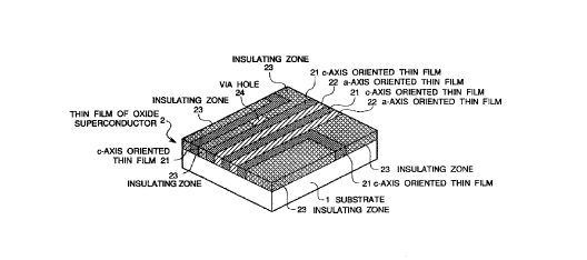
The superconductit)g circuit of ~igure 1 has a thin film layer 2 of
oxide su,~ol~ductor deposited on a substrate l~ The thin film layer 2 of
oxide superconductor comprises c-axis oriented thin film zones 21, a-axis li
oriented thin film zones 22, insulation zones 23 in which
2 6superc~nd~lctivity is lost and viaholes 24
The c-axis oriented thin film zones 21 provide superco.lducting
wiring lines in which a superconducting current propagates in parallel
with a surface of the substrate 1~ The a-axis oriented thin film zones 22
12
CA 020~4796 l997-l2-lO
provide superconducting wiring lines in which superconducting current
flow perpendicularly to and/or in parallel with the surface of the
substrate 1.
Figure 2 is a drawing illustrating a relation in the directions of
S crystal orientation in two wiring lines A and B deposited on a plane P.
The wiring line A corresponds to the c-axis oriented thin film zones 21
shown in Figure 1, while the wiring line B corresponds to the a-axis
oriented thin film zones 22 shown in Figure 1. It should be noted that, in
this example, there is no difference between the a-axis oriented thin film
10 and a b-axis oriented thin film in the oxide superconductors to which the
present invention is applicable because the oxide superconductors have
layered structures in which superconducting current flow dominantly to a
direction which is perpendicular to the c-axis.
In the insulation zones 23, no superconducting current flow. The
15 viaholes 24 are used to connect layers in a stacked multi-layered circuit
(not shown).
Example 2
Figure 3A to Figure 3F are illustrative drawings showing successive
2 0 steps for fabricating the superconducting circuit shown in Figure 1. In
this Example, a compound oxide superconductor of Y-Ba-Cu-O system is
used as the oxide superconductor.
At first, a substrate I having a smooth surface is prepared. In this
Example, the substrate 1 (Figure 3A) consists of a silicon substrate la
25 having a buffer layer Ib which is composed of an under-layer of
MgA1203 having a thickness of 350 nm deposited by chemical vapour
deposition (CVD) technique and an upper-layer of BaTiO3 having a
thickness of 75 nm deposited by sputtering technique. MgO (100)
13
2~479G
substrate, CdNdAl04 substrate or the like can be preferably used in place
of the silicon substrate.
On the buffer layer of the substrate 1, a thin film 2 of oxide
superconductor having a thickness of more than 200 nm as is shown in
5 Figure 3B is deposited. This thin film 2 can be prepared by an off-axis
s~Julleril~g technique, a reactive evaporation technique or ~e like. In this
Example, the thin film 2 of oxide superconductor is prepared by the
off-axis sputtering technique under the presence of a mixed s~ulle-lng gas
of Ar + ~2 (volume ratio of 9: 1) of l0 Pa. 'rhe substrate is heated at
10 700 ~C so that the clystals produce a c-axis orientated thin film of oxide
superconductor in which c-axis is oriented perpendicularly to the surface
of the substrate.
Then, as is shown in Figure 3C, a photoresist layer 3 having a
predetermined pattern is coated on the thin film 2 of oxide
15 superconductor obtained.
After the photoresist layer 3 is cured, exposed areas which are not
covered with the photoresist 3 are removed by a dry-etching technique
such as reactive ion etching and argon milling or by a wet etching
technique such as treatment with phosphoric acid or hydroch]oric acid in
20 such a manner that patterned superconducting wiring lines 2c consisting
of the c-axis oriented thin film and insulation zones 23 are left as is shown
in Figure 3D. The insulation zones 23 can be produced by deoxygenation
trea~ment.
At the resulting etched areas, another superconducting wiring lines
25 each being made of an a-axis oriented thin film will be produced in next
stage. Thus, as is shown in Figure 3E, an a-axis oriented thin film 2a of
the same oxide superconductor is deposited on the surface of the su~strate
l on which the patterned superconducting wiring lines 2c consisting of the
14
2 ~ 6
c-axis oriented thin film have been deposited. This thin film 2a of oxide
superconductor also is prepared by the off-axis sputtering technique under
the presence of a mixed sputtering gas of Ar + ~2 (volume ratio of 9: 1)
of 10 Pa but the su~strate is heated at a temperature of lower than 650 ~C
5 so that the thin film of oxide superconductor 2a deposited becomes an a-
axis oriented thin film.
After then, a surface of the a-axis oriented thin film 2a is smoothed
by a dry etching technique such as reactive ion etching or argon milling to
obtain a superconducting circuit according to the present invention as is
10 shown in Figure 3F~ Namely, both surfaces of the superconducting lines
2c made of c-axis oriented thin film and of the superconducting lines 2a
made of a-axis oriented thin fi]m make a planar flat surface or a common
plane.
Tn practice, an interlayer insulator layer is deposited on the
15 resulting superconducting circuit shown in Figure 1 according to the
present invention before the latter is passed to next stages for completing
the superconducting circuit into a desired superconducting device.
The insulation zones 23 shown in Figure 1 can be prepared by
deoxygenation of the thin film 2 of oxide superconductor. Namely, after
20 predetermined areas of the thin film 2 of oxide superconductor are
protected with patterned photoresist or insulator, remaining exposed areas
are subjected to a treatment of deox),genation so that the exposed areas are
changed into non-superconductor.
2 5 Rx~ le 3
Figure 4 is an illustrative perspective view of another example of
the superconducting circuit according to the present invention.
20547g6
The superconducting circuit of Figure 4 has a thin film layer 2 of
oxide superconductor deposited on a substrate l. The thin film layer 2 of
oxide superconductor comprises c-axis oriented thin film zones 2c, a-axis
oriented thin film zones 2a and in~ tion zones 2b.
The c-axis oriented thin film zones 2c provide superconducting
wiring lines in which a superconducting current propagates in parallel
with a surface of the substrate l. Ill this su~r~ull~lu~tin~ wiring lines 2c,
superconducting current can flow along two directions "Y" and "X".
Lines along the direction "Y" is called the first supercollducting wiring
line 2c', while lines along the direction "X" is called the second
~u~rcollducting wiring line 2c".
The a-axis oriented thin film zones 2a provide shield zones each
functions as a shield to separate respective superconducting wiring lines
2c~ In fact, the shield zones 2a prevent crosstalk between adjacent
su~erconducting wiring lines 2c in which superconducting current ca
flow along any one of two directions "Y" and "X".
The insulation zones 2b are arranged at opposite sides of each
second ~;u~e[conducting wiring line~ The insulation zones 2b can be
produced by deoxygenation treatment which is effected on selected
20 portions of the a-axis oriented thin film 2a~
Example 5
Figure SA to Pigure SP are illustrative drawings showing successive
steps for fabricating the superconducting circuit shown in Figure 4. In
2 5 tllis Example, a compound oxide superconductor of Y-Ba-Cu-O system is
used ~s the oxide superconductor.
At first, a substrate l having a smooth surface is prepared. In this
Example, the substrate l (Figure SA~ consists of a silicon substrate la
16
2~7~6
having a buffer layer lb which is composed of an under-layer of
MgAl2O3 having a thickness of 350 nm deposited by chemical vapour
deposition (CVD) technique and an upper-layer of BaTiO3 having a
thickness of 75 nm deposited by sputtering technique. MgO (100)
substrate, CdNdA104 substrate or the like can be preferably used in p1ace
of the silicon substrate.
On the buffer layer of the substrate l, a thin film 2 of oxide
superconductor having a thickness of more than 200 nm as is shown in
Figure SB is deposited. TlliS thin film 2 can be prepared by an off-axis
1~ slJu~ g technique, a reactive evaporation technique or the like. In thisExample, the thin film 2 of oxide superconductor is prepared by the
off-axis sputtering technique under the presence of a mixed sputtering gas
of Ar + ~2 (volume ratio of 9: 1) of 10 Pa. The substrate is heated at a
temperature which is higher than 700 ~C so that the crystals deposited
produce an c-axis orientated tl2in film of oxide superconductor in which
c-axis is oriented perpendicularly to the surface of the substrate.
Then, as is shown in Figure SC, a photoresist layer 3 having a
predetermined patter is coated on the thin film ~ of oxide superconductor
obtained.
After the photoresist layer 3 is cured, exposed areas which are not
covered with the photoresist 3 are removed by a dry-etching technique
such as reactive ion etching and argon milling or by a wet etching
technique such as treatment with phosphoric acid or hydrochloric acid so
as to produce a patterned superconducting wiring lines 2c consisting of
the c-axis oriented thin film as is shown in Figure SD.
Then, as is shown in Figure se, an a-axis oriented thin film 2a of
the same oxide superconductor is deposited on the surface of the substrate
1 on which the patterned superconducting wiring lines 2c consisting of the
CA 020~4796 1997-12-10
c-axis oriented thin film have been deposited. This thin film 2a of oxide
superconductor also is prepared by the off-axis sputtering technique under
the presence of a mixed sputtering gas of Ar + ~2 (volume ratio of 9: 1)
of 10 Pa but the substrate is heated at a temperature which is not higher
S than 650 ~C so that the thin film of oxide superconductor 2a deposited
becomes a-axis oriented thin film. In this a-axis oriented thin film, it is
preferable that its c-axis is also well-ordered.
After then, a surface of the a-axis oriented thin film 2a is smoothed
by a dry etching technique such as reactive ion etching or argon milling to
10 obtain a superconducting circuit according to the present invention as is
shown in Figure SF. Namely, both surfaces of the superconducting
wiring lines 2c made of c-axis oriented thin film and of the shield zones
2a made of a-axis oriented thin film make a flat planar surface or a
common plane.
In actual applications, an interlayer insulator layer is deposited on
the resulting superconducting circuit shown in Figure 4 according to the
present invention before the latter is passed to next stages for completing
the superconducting circuit into a desired superconducting device.
The insulation zones 2b shown in Figure 4 can be prepared by
20 deoxygenation treatment of the thin film 2 of oxide superconductor.
Namely, after predetermined areas of the thin film 2 of oxide
superconductor are protected with patterned photoresist or insulator,
remaining exposed areas are subjected to deoxygenation treatment so that
the exposed areas are changed into non-superconductor. The
2 S deoxygenation treatment can be effected by local heating by means of a
laser beam or a focussed ion beam.