Note: Descriptions are shown in the official language in which they were submitted.
CA 020~4934 1999-04-20
ELECTRO-OPTICAL DETECTOR ARRAY AND METHOD OF M~T~G SAME
The present invention relates generally to
electro-optical dLetector arrays and more particularly to
an electro-optical del:ector array having front faces of
semiconductor elements illuminated by the optical energy,
and to a method of making same.
SemicondLuctor electro-optical detectors are either
of the photovolt:aic or photoresistive type. Different
types of electlo-optical detectors are employed for
different wavelength regions from infrared through
ultraviolet. For example, photovoltaic electro-optical
detectors for the infrared wavelength range from
approximately 8 to 12 microns and 1 to 5.6 microns are
frecluently made of mercury cadmium telluride (HgCdTe) and
indium antimonide (InSb), respectively. The specific
construction of inldium antimonide electro-optical
detectors is desc:ribed, for example, in commonly assigned
U.S. Patents 3,483,096, 3,554,818 and 3,577,175. While
the following descriptiLon is made for InSb electro-optical
detectors, the invention in many of its broade~t aspect~
is not limited to this material.
2 2 0 ~
Single element devices, as disclosed in the
aforementioned patents, typically include a P-N
junction wherein an N-doped bulk substrate carries a P-
doped region that is exposed to an optical energy
source being detected. Usually, the P-N junction is no
greater than about 4 microns from the surface of a P-
type region on which the optical energy to be detected
is incident. In other words, the P-type region exposed
to the optical radiation to be detected has a thickness
of no greater than about 4 microns. For certain InSb
devices, the P-N junction is closer than 0.5 microns to
the surface of the P-type region exposed to the
radiation. The P-type region is desirably positioned
so that the optical radiation is directly incident
thereon to enable photo-generated charge carriers
formed in the P-type region to diffuse, somewhat
uninterrupted, to the junction. Even in this
configuration, a significant amount of optical energy
penetrates through the P-type region into the P-N
junction where some additional charge carriers are
generated and on into the N-type region where still
more charge carriers are generated. As long as this
absorption in the n-type material does not occur too
far away from the junction, the resulting charge
carriers also diffuse back to the junction. In
addition, this arrangement enables optical energy that
is not absorbed in the P-type region to reach the P-N
junction directly. Thereby, efficiency in converting
optical energy to electric energy is relatively high if
the P-doped region of an indium antimonide detector is
arranged such that the optical energy is incident on
the P-type region.
While these characteristics have long been known,
to our knowledge, they have not been achieved when
relatively large InSb electro-optical semiconductor
detector arrays have been manufactured. In the large
3 ~ Q 5 ~
InSb array prior art of which we are aware, it has been
the practice to illuminate the relatively thick N-type
doped bulk substrate semiconductor material, i.e., the
"back" face of the array has been illuminated. The
thickness of the illuminated N-type doped bulk
substrate is typically 10 microns which increases the
probability that photogenerated charge carriers will
interact with crystal defects or other charge carriers
in the N-type bulk substrate. This is particularly
true of the shortest wavelength energy to which the
optical detector is exposed because the shortest
wavelength energy is absorbed closest to the back face,
and the resulting photogenerated charge carriers must
travel the greatest distance to the P-N junction. In
addition, very little, if any, of the optical energy in
the 1-4 micron region can propagate unimpeded to the P-
N junction through the bulk material.
The construction and manufacturing method of a
typical prior art indium antimonide, photovoltaic
detector array are illustrated in Figures 1 and 2. In
this and other prior art arrangements, the optical
energy to be detected is first incident on the
relatively thick (about 10-20 microns) N-type bulk
substrate. Hence, the distance between the P-N
junction and the surface on which the optical radiation
to be detected is first incident is approximately 10-20
microns. For the shortest wavelengths in the 1-5.6
micron band to be detected, i.e., between 1 and 3
microns, there is a relatively low quantum efficiency
because photogenerated charge carriers created in the
N-type bulk substrate in response to the incident
optical energy do not proceed in an unimpeded manner to
the N-type bulk substrate. Instead, the free charge
carriers resulting from absorption of optical energy
photons frequently interact with the InSb crystal
lattice and crystal defects prior to reaching the P-N
4 2 ~ 5 ~
junction, causing the carriers to lose energy and
recombine with other carriers of the opposite type and
therefore go undetected. In addition, very little of
the shortest wavelength energy is able to reach the
junction without being absorbed in the N-type material
and create photogenerated carriers therein.
In the prior art arrangement illustrated in
Figures 1 and 2, an indium antimonide N-type bulk
substrate 23, having a thickness of approximately 15
mils with an array of P-type regions 24 formed thereon,
is connected to multiplexer substrate 25 by indium
columns 26, which can be grown on metal contact pads
(not shown), typically of gold, nickel or chromium for
the P-type regions or on the multiplexer substrate or
on a combination of both. A P-N junction, forming a
diode, exists at each location of P-type region 24 on
N-type bulk substrate 23. After the detector assembly
including N-type bulk substrate 23 and an array of P-
type regions 24, formed by gaseous diffusion or ionic
bombardment, has been connected to multiplexer
substrate 25, the bulk material substrate is
mechanically and/or chemically thinned and polished to
a thickness of approximately 10 microns, as illustrated
in Figure 2. Multiplexer substrate 25 includes
electronic circuitry having switching elements with
substantially the same topography as the topography of
P-type regions 24. The electronic circuitry in
multiplexer substrate 25 selectively reads out the
signal from a selected diode of the electro-optical
detector array through the indium bump to one or a few
common signal leads on the multiplexer chip. This
causes readout of the optical energy incident on a
surface of N-type bulk substrate 23 corresponding
generally with the P-type region 24 connected to the
indium column or bump 26 which is selected by the
circuitry on multiplexer N-type bulk substrate 25.
205~
To withstand the mechanical forces during and
after thinning, an epoxy bonding agent is injected
between the array including N-type bulk substrate 23
and P-type regions 24 and multiplexer 25. The bonding
agent fills the space between indium columns or bumps
26.
In use, the structure of Figure 2 is arranged so
that the optical energy is initially incident on N-type
bulk substrate 23. The optical energy creates free
charge carriers, an electron-hole pair for each photon
absorbed, in bulk substrate 23. If the minority
carrier, i.e., the hole in N-type indium antimonide N-
type bulk substrate 23, recombines with a majority
carrier, no current results and the optical energy is
not detected. If, however, the minority carrier
diffuses to and crosses the junction between N-type
bulk substrate 23 and a particular P-type region 24,
current is produced in the P-type region.
Whether a minority carrier diffuses across the
junction is a function of (1) how far away from the
junction the electron-hole pair is at the time it is
created by the incident optical energy, (2) the
diffusion length in bulk material 23, and (3) the
density of the bulk material defects which act as
recombination centers. These defects can exist before
processing is performed. However, other defects are
created by several of the many processing steps, e.g.,
by ion implantation, thinning and/or bump bonding. In
general, detector efficiency in converting optical
energy to electrical energy decreases as the distance
between the junction and the surface on which the
optical energy is initially incident increases.
Thinning and polishing operations performed on N-
type bulk substrate 23 place severe stresses on the
detector and often result in N-type bulk substrate
cracking. Polishing compounds and mechanical abrasion
CA 020~4934 1999-03-30
used to thin N-type bulk substrate 23 result in micro-
crystalline damage on the surface of and into N-type
bulk substrate 23 on which the optical energy is
initially incident. The microcrystalline damage has
severe detrimental effects on the electrical
characteristics of the array. The resulting degradation
of the bulk material in N-type bulk substrate 23 on
which the optical energy is incident produces a high
surface recombination rate in the N-type bulk substrate
23, lowering quantum efficiency dramatically,
particularly at the shortest wavelengths which are
absorbed close to the surface of N-type bulk substrate
23.
The detector arrays are usually operated at
cryogenic temperatures, in the liquid helium or liquid
nitrogen range. While lower quantum efficiencies at
short wavelengths may not occur in InSb arrays at liquid
nitrogen temperatures, the diffusion length (mentioned
above) decreases dramatically as temperature is lowered
further such that at liquid helium temperature ranges
(of interest to astronomers), the performance of the
prior art devices is degraded. Also, operation at
liquid nitrogen temperatures causes the arrays to
undergo severe mechanical strain due to thermal
expansion mismatch between the bulk material of N-type
bulk substrate 23 and multiplexer substrate 25. The
very thin bulk material of N-type bulk substrate 23
cannot always accommodate the induced strain and is
subject to breakage or may become deformed to cause
bonds between indium columns 26 and N-type bulk
substrate 23 or the pads thereon to fail.
An additional disadvantage of the prior art
methods is that the th;nning process is performed
after sawing the detector wafer into individual chips
and after bump bo~;ng occurs. As an example, if
there are ten arrays on a wafer, the thinning pro-
cess is performed ten different times, resulting in an
7 2 $~
expensive processing technique.
It is, accordingly, an object of the present
invention to provide a new and improved electro-optical
detector array and to a method of making same.
Another object of the invention is to provide a
new and improved electro-optical detector array having
P-N junctions in very close proximity to a surface on
which optical energy is initially incident, and to a
method of making same.
An added object of the invention is to provide a
new and improved electro-optical detector for infrared
energy in the 1-5.6 micron wavelength band, which
detector has relatively high quantum efficiency for
wavelengths throughout the aforementioned spectrum, and
to a method of making same.
A further object of the invention is to provide a
new and improved electro-optical detector adapted to be
used in cryogenic temperature environments, but which
has stable mechanical and electrical properties even
though the array is subject to temperature cycle
extremes, and to a method of making same.
Still another object of the invention is to
provide a new and improved electro-optical detector
array wherein all detector processing is performed
prior to connecting the wafer to external control
circuitry, e.g., a multiplexer N-type bulk substrate.
An additional object of the invention is to
provide a new and improved indium antimonide detector
array having relatively high quantum efficiency over
the entire spectrum of use for such arrays, wherein the
array has stable mechanical and electrical properties,
even though it is operated at cryogenic temperatures
and is subject to cycling between those temperatures
and ambient temperatures, and to a method of making
same.
Still another object of the present invention is
CA 020~4934 1999-03-30
to provide a new and improved indium antimonide
detector array wherein P-type material in the indium
antimonide i8 positioned 80 that infrared optical
energy to be detected is initially incident on the P-
type material, instead of on the N-type material of
the detector, and to a method of making same.
In accordance with one aspect of the present
invention an electro-optical detector comprises a
dielectric backing transparent to optical energy to be
detected, in combination with an array of
semiconductor diodes on the backing, which diodes have
an electrical property affected by optical energy
incident thereon and include a junction separating
first and second differently doped regions, wherein
the first and second regions are positioned on the
backing and are arranged 80 that the optical energy to
be detected and propagating through the backing is
incident on the first region prior to being incident
on the second region. The first regions have a
thickness that is a function of the lifetime of
carriers produced in the first regions in response to
photons of the optical energy and the capture cross
section of the optical energy photons by the lattice
such that the carriers reach the junction without
interacting with other possible carriers in the first
regions or the photons traverse the first regions
without being absorbed; for InSb, this thickness is
less than one-half micron.
In accordance with another aspect of the inven-
tion an electro-optical detector comprises a dielectric
backing transparent to optical energy to be detected,
in combination with an array of indium antimonide semi-
conductor diodes on the backing, which diodes
include a junction separating P-type and N-type doped
regions that are positioned on the backing and arranged
so that the optical energy to be detected and
propagated through the backing is incident on the P-
type doped region prior to being incident on the N-type
doped region.
In accordance with an additional aspect of the
invention, an electro-optical detector comprises a
dielectric backing transparent to optical energy to be
detected in combination with an array of semiconductor
diodes on the backing, which diodes have an electrical
property affected by optical energy incident thereon
and include a junction separating the first and second
differently doped regions, wherein the first and second
regions are positioned on the backing and arranged so
that the optical energy to be detected and propagating
through the backing is incident on the first region
prior to being incident on the second region. Both
regions of adjacent ones of the diodes are spaced from
each other, to basically form islands in the backing.
In accordance with a further aspect of the
invention an electro-optical detector comprises a
dielectric backing transparent to optical energy to be
detected in combination with an array of semiconductor
diodes on the backing, which diodes have an electrical
property affected by optical energy incident thereon
and include a junction separating first and second
differently doped regions, wherein the first regions
are positioned on the backing and are arranged so that
the optical energy to be detected and propagating
through the backing is incident on the first region
prior to being incident on the second region. The
second regions are formed of bulk material, while the
first regions are layers formed by diffusing a dopant
into the bulk material, or by implanting ions into the
bulk material.
In a preferred embodiment, metal on the dielectric
backing electrically connects the first regions
CA 020~4934 1999-03-30
together without interfering substantially with the
optical energy incident on the first region, i.e., on
the P-type region of the indium antimonide detector.
In one embodiment, the metal is arranged as a grid of
intersecting strips extending in mutually perpendicular
directions. In a second embodiment, the metal is
arranged as a film having windows for enabling the
optical energy to be detected to be incident on the
first regions.
A multiplexer integrated circuit substrate extends
parallel to the backing and includes an array of
elements for selective readout of the electrical property
of the diodes. The readout elements and diodes have
approximately the same topography so that corresponding
ones of the elements and diodes are aligned. An array
of metal (preferably indium) bumps or columns connects
the corresponding adjacent elements and diodes.
In accordance with still a further aspect of the
invention, a method of making a semiconductor optical
detector array comprises the steps of forming an array
of P-N junctions on a bulk semiconductor of a first
conductivity type (N-type material for InSb bulk
material), such that the junctions are close to a
surface of the bulk semiconductor. The junctions are
between the first conductivity type bulk semiconductor
and semiconductor regions of a second conductivity type
(P-type material for an InSb array). A portion of the
semiconductor regions is metallized. The semiconductor
regions are bonded to a transparent backing so that an
optical path subsists through the backing to at least a
segment of the semiconductor regions. The thickness of
the N-type bulk substrate is reduced while the
semiconductor regions are bonded to the backing. The
reduced thickness N-type bulk substrate is etched to
form an array of diode islands. Each of the different
diode islands includes a corresponding region of the
CA 020~4934 1999-03-30
bulk semiconductor, a junction, and the second
conductivity type semiconductor. Electrodes are
attached to the first conductivity type regions of the
islands.
The above and still further objects, features and
advantages of the present invention will become
apparent upon consideration of the following detailed
description of several specific embodiments thereof,
especially when taken in conjunction with the
accompanying drawings.
Figures 1 and 2, described supra, are
illustrations of a prior art indium antimonide
infrared detector array;
Figure 3 is a side view of one preferred
embodiment of an indium antimonide detector array in
accordance with the present invention;
Figures 4-7 are illustrations of intermediate
structures used to form the indium antimonide detector
array of Figure 3;
Figure 8 is a side sectional view of a further
embodiment of the present invention; and
Figure 9 is a plan sectional view through lines
9-9, Figure 8.
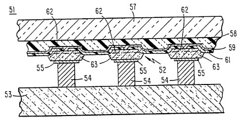
Reference i now made to Figure 3 wherein
photovoltaic indium antimonide infrared detector diode
array 52 for radiation in the wavelength region from
1 to 5.6 microns is illustrated as being mounted on
optically transparent backing 51. Multiplexer
integrated circuit substrate 53, that extends parallel
to backing 51, is electrically connected to the diode~
of the array by indium columns 54.
The diodes of array 52 are arranged on backing 51,
4 q ~ ~
12
transparent to the optical energy to be detected, so
that P-type doped regions 62 of the diodes have the
optical energy to be detected incident on them prior to
the energy being incident on N-type bulk substrate
regions 63 of the diodes in the array. The diodes of
the array are formed as islands, such that adjacent
diodes are spaced from each other by dielectric. P-N
junctions of the diodes of array 52 between P-type and
N-type regions 62 and 63 are no more than approximately
four microns (and are typically less than about a half
micron) from the surface of each diode on which the
optical energy to be detected is initially incident.
Because of the close distance of the individual
junctions to the surface on which the optical energy is
initially incident, charge carriers formed in P-type
regions 62 diffuse directly to the junction to cause
efficient transfer of optical energy into electrical
energy by the semiconductor diodes of array 52,
throughout the wavelength region of interest, including
the short wavelength end of the spectrum. Current
flowing in the N-type regions of the diodes of array 52
as a result of the incident optical energy is
transferred to elements in multiplexer 53 by way of
metal contact pads 55 on N-type regions 63, and the
connections of the metal pads to the multiplexer
elements by way of indium columns 54.
Dielectric backing 51, transparent to the optical
energy to be detected, includes dielectric plate 57
(e.g., of sapphire or gallium arsenide) which serves as
a window and has a backface covered with epoxy glue
layer 58, which overlays metal grid layer 59, typically
formed of intersecting gold strips extending in
mutually perpendicular directions. Metal grid layer 59
connects each of P-type regions 62 to a reference
potential level, such as ground. The vast majority of
metal grid 59 extends over oxide layer 61, preferably
13 2~4~3~
silicon monoxide or silicon dioxide, which overlays the
vast majority of each of P-type regions 62 of the
indium antimonide diodes of array 52 and is transparent
to the optical energy to be detected, as is plate 57.
Metal pads 55 are deposited on the faces of N-type
regions 63 remote from the faces of P-type regions 62
on which the optical energy to be detected is initially
incident.
Metal grid 59 extends through a portion of oxide
layer 61 to establish contact with the front face of
each of P-type regions 62. The percentage of the area
of each front face of region 62 covered by metal grid
59 is relatively small so that the metal grid does not
shadow a substantial portion of the otherwise exposed
front face of P-type regions 62. The diodes of array
52 and metal grid 59 are preferably arranged in a
square matrix, although this is not necessarily the
case; e.g., the diodes of array 52 can be arranged in a
linear array, a rectangular array or even in a circular
array. Usually at least 16 diodes comprise an array of
interest for the present invention.
P-type region 62, N-type region 63 and the
associated junction of each indium antimonide diode of
array 52 are arranged so that almost all of the 1-2
micron radiation to be detected is either absorbed in
the P-type region or the junction, while some of the 2
micron and longer wavelength radiation penetrates
through the P-type region and the junction to the N-
type region. To this end, the distance to the
electrical P-N junction between regions 62 and 63 from
the face of P-type region 62 contacting oxide layer 61
is no more than 4 microns and is likely to be 0.5
micron or less, while the thickness of N-type region 63
is between 5 and 20 microns. This construction enables
a significant number of photons to be absorbed in or
near the junction such that charge carriers resulting
14
from the incident optical radiation diffuse to the
junction without recombining. Thereby, there is
improved quantum efficiency in transferring optical
energy to electrical energy, particularly in the short
wavelength 1 to 2 micron region.
Oxide layer 61 engages upper and side surfaces of
P-type regions 62, as well as side surfaces of N-type
regions 63, to provide an electrical insulating layer
for the P-N junctions. In addition, oxide layer 61
prevents etchants used to isolate the indium antimonide
diodes of array 52 into islands, as described infra,
from attacking metal grid layer 59.
A preferred method of forming the structure
illustrated in Figure 3 is illustrated in Figures 4-7.
Initially, as illustrated in Figure 4, bulk N-type
indium antimonide substrate 71, having a thickness of
approximately 10 mils, for example, has P-type regions
62 formed thereon by using a gaseous deposition process
or by ion bombardment. Oxide layer 61 and metal grid
59 are then deposited in sequence on the exposed, upper
face of N-type bulk substrate 71 and P-type regions 62
to form the structure, somewhat as illustrated in
Figure 5. (Figure 5 is a schematic representation of
metal grid layer 59, as well as the top surfaces of P-
type regions 62 and N-type bulk substrate 71; oxide
layer 61 is not illustrated, for clarity.) Thereby,
there is formed a matrix of square mutually spaced P-
type regions 62 which overlay the top face of N-type
bulk substrate 71, leaving a row and column matrix
arrangement of the N-type bulk substrate that is not
covered by the P-type regions. Metal grid 59 overlays
a portion of illustrated faces of P-type region 62 and
N-type bulk substrate 71.
Plate, i.e. window, 57 is bonded to the exposed
surfaces of metal grid 59 and oxide layer 61 by epoxy
glue layer 58 to form the structure illustrated in
2~
Figure 4. Typically, anti-reflective coatings are
provided for the indium antimonide face exposed to the
optical energy, in a manner well known to those skilled
in the art. For clarity purposes, the anti-reflective
coatings are not illustrated.
After the structure illustrated in Figure 4 has
been fabricated, the thickness of N-type bulk substrate
71 is reduced, to about 10 to 20 microns, as
illustrated in Figure 6. The thickness of N-type bulk
substrate 71 is reduced, i.e., the N-type bulk
substrate is thinned, by conventional mechanical and/or
chemical means. An etchant mask is then formed on the
exposed regions of bulk substrate layer 71
corresponding generally to the oxide layer regions that
contact N-type bulk substrate 71, Figure 6. An indium
antimonide wet chemical etchant is then applied to the
etchant mask and the exposed face of N-type bulk
substrate 71, to cause trenches to be formed between
the N-type regions 63, as illustrated in Figure 7.
Dry, i.e., plasma, etching or ion beam milling can also
be used to form trenches in the detector material; the
trenches isolate individual islands of the detector
material to form isolated detector diodes. Thereby,
multiple spaced diodes, each including P-type region 62
and N-type region 63, are formed. The N-type regions
of all the diodes are mechanically and electrically
spaced from each other; the P-type regions of the
diodes are all mechanically spaced from each other, but
are electrically connected to each other by metal grid
59.
After the structure illustrated in Figure 7 has
been manufactured, metal ohmic contact pads 55 (Fig. 3)
are deposited on N-type regions 63 and columns or bumps
54 are grown on the metal pads. In particular,
multiplexer substrate 53 is connected to the diodes of
array 52 by growing indium columns or bumps 54 on the
16 ~ 3 ~
metal pads and/or regions of the multiplexer
corresponding with and topographically aligned with the
diodes of array 52. Then the wafer is sawed into
individual arrays that are bump-bonded to multiplexer
readouts.
In contrast to previous structures, which were P-
type indium antimonide "islands" with a common N-type
indium antimonide N-type bulk substrate (commonly
referred to as a "P on N" structure), the structure of
the present invention consists of islands each having
an N-type region on a P-type region to form a separate
diode having a P-N junction. In the prior art, the
optically produced carriers must traverse many microns
of N-type indium antimonide to reach a carrier
collection region. In the InSb embodiment of the
present invention, the optically produced carriers only
must traverse 0.5 microns (or less) of P-type region 62
to reach the carrier collection region. In the present
invention, the P-type material in the islands is
electrically connected by metal grid pattern 59 and all
of the diode islands are mechanically spaced from each
other by etching the material between the P-type
layers. Because of these factors, the present
invention is considered as an "N on P" device.
The only reason, in the present invention, for
thinning the N-type bulk substrate is to allow the
etching step, i.e., removal of a substantial amount
material between the P-type regions, to occur quickly
and with minimal lateral etching. Because the device is
illuminated from the "front," i.e., P-type side,
mechanical damage arising from machining the N-type
bulk material does not adversely affect the optical and
electrical detection properties of the array. The P-
type region, in many instances, extends less than 1
micron from the surface of the InSb on which the energy
to be detected is incident. By arranging the carrier
17 2~ 9~
collection region to be so close to the surface on
which the energy to be detected is incident, all of the
problems of minority carriers having to diffuse "long"
distances (approximately 10 microns) through N-type
material with high concentrations of recombination
centers are eliminated.
In the present invention, the detector material is
basically processed in wafer form, thereby improving
planarity and thickness control. In many cases, the
manufacturing procedure also eliminates the stress from
N-type bulk substrate 71 since the detector and
multiplexer N-type bulk substrates can be made of the
same material or of materials with the same or nearly
the same thermal coefficients of expansion. Hence,
there is virtually no stress to cause the bonds to
indium columns 54 to fail. Further, there is complete
electrical isolation of the detector diodes of array 52
because there is no electrical contact between adjacent
N-type regions 63, thereby eliminating optical and
electrical crosstalk between the diodes of array 52.
By physically removing the indium antimonide between
adjacent diodes of the array, charge carriers that
might diffuse sidewise are decoupled from adjacent
diodes.
Isolating the individual indium antimonide diode
detector islands removes thermal expansion stresses
from the detector material. Thermal stress problems in
the very brittle indium antimonide detector material
are relieved because of the small size of the
individual islands forming detector array 52. In the
prior art, thermal stress problems frequently occurred
because of the differential expansion of the indium
antimonide N-type bulk substrate relative to the
multiplexer N-type bulk substrate. In the prior art,
the bulk indium antimonide has an area comparable to
the area of the multiplexer so that expansion of the
18
indium antimonide relative to the multiplexer causes
stresses to be established in the indium antimonide.
Because the diodes in the present invention are formed
as spatially isolated, small islands, the expansion of
any diode element is negligible relative to the
expansion of the multiplexer.
Hence, the structure of Fig. 3 is made by
beginning with the normal process for making InSb diode
arrays, starting with a bulk N-type InSb wafer. The
surface of the wafer is then modified by diffusion or
ion implantation to create a P-type layer. In the
"mesa" method of forming diode arrays, a photomask and
etch process is used to delineate individual P-type
mesa regions by etching away the P-type (and some N-
type) InSb between the desired P-type areas. The
etching is very shallow, on the order of 1 to 4
microns, as the thickness of the P-type region is
usually only about 0.4 microns. The edge of the P-N
junction of each diode is exposed on the side walls of
each mesa. Oxide and metal patterns are then deposited
on this surface just prior to attachment to the
transparent backing. Subsequent backside thinn;ng and
etching are performed in accordance with the present
invention, as previously described in connection with
Figs. 3-7.
The principles of the invention are also
applicable to "mesa-less" processes and structures, as
illustrated in Figs. 8 and 9. The "mesa-less" process
also begins with an N-type wafer having a P-type layer
formed on the surface by diffusion or ion implantation.
In the "mesa-less" process, the etch step to delineate
individual P-type mesa regions is omitted. The oxide
and metal layers are deposited on the P-type surface
just prior to attachment to the transparent backing.
Thinning and backside etching proceed as described
supra in connection with Figs. 6 and 7. The individual
19
diodes are formed as the backside etch removes all the
InSb (both N-type and P-type) between adjacent diodes.
The edge of the P-N junction of each diode is thereby
exposed on the side wall of the island forming each
diode, as generally shown by the side view of this
structure in Fig. 8, wherein N-type regions 63 are
formed from an N-type bulk substrate having no mesas.
P-type regions 62 are formed on the substrate as
described suPra with the exception that the "window"
metal pattern is shown. Subsequent deposition of metal
contact pads and growth of indium columns is the same
for both styles of diode formation.
In the embodiment of the invention illustrated in
Figures 8 and 9, metal grid 59, Fig. 3, is replaced
with metal layer 81 having windows 82 therein. Windows
82 are positioned over the exposed faces of P-type
regions 62 and have an area slightly less than the area
of the P-type regions. Thereby, the P-type regions are
connected together by metal layer 81. Because windows
82 and metal layer 81 have an area less than the areas
of P-type regions 62, all of the P-type regions are
connected together. The N-type regions of the diodes
of detector array 52 are electrically isolated from
metal layer 81 by oxide layer 61. Because the area of
windows 82 can be controlled more accurately than the
area of the P-type regions or the N-type regions, the
uniformity of the response to optical energy is
increased relative to the structure of Figure 3. The
window structure of Figs. 8 and 9 can be used in a mesa
structure of the type illustrated in Fig. 3.
While there have been described and illustrated
several specific embodiments of the invention, it will
be clear that variations in the details of the
embodiment specifically illustrated and described may
be made without departing from the true spirit and
scope of the invention as defined in the appended
~4~
claims. For example, in the illustrated embodiments
there is only a small amount of shadow interference of
the incident optical energy due to metal grid 59 or
metal layer 81. In other embodiments, there can be
considerably greater shadow interference (e.g., up to
99%).