Note: Descriptions are shown in the official language in which they were submitted.
2~55096
1 68086-465
BACKGROUND ART
1. Field of the Invention:
The æubject invention relates to storage assemblies
having electronic locks. More particularly, the subject invention
relates to electronically programmable locking storage assemblies
having limited and varying access.
2. Description Of Related Art:
As the size of a company grows, so does the need to
limit the access of information only to those employees who have a
need to use the information. The limitation of access helps to
focus the employees on their particular tasks and increases the
time needed to locate information when it is out of its storage
location. In addition, limiting the access of information
increases security of the information.
We have previously devised an electronic interlock
system for storage units such as file cabinets. The electronic
interlock is a lock totally independent of any other file cabinet
although it may have a port to allow electronic communication with
a computer, such as a personal computer, exterior therefrom.
The prior art does not disclose an electronic lock used
for office furniture wherein the programmable capabilities of the
electronic lock are removable.
`- A -~
Meridian P-306 -2- ZO ~9 6
United States Patent Number 4,083,424 to
von den Stemmen et al, issued on April 11, 1978,
discloses a portable housing unit having keyboard for
receiving codes, which are input by the user, to
unlock the electronic lock of a vehicular cargo
space. This portable housing unit does not, however,
have any capability of programming new or existing
codes into or out of the vehicular lock.
United States Patent Number 3,812,403 to
Gartner, issued on May 21, 1974 discloses an
electronic locking system for a door comprising a
door and a door jam. A removable push-button switch
is inserted into the locking system and a locking
sequence is transferred to the locking system. If
the sequence matches, the door is unlocked. This
system, however, does not disclose any ability to
program the door locking system via the push button
switch.
United States Patent Number 4,250,533 to
Nelson, issued on February 10, 1981 discloses a
security system having one programmable key. The key
has a programmable read only memory chip (PROM),
which has several codes therein. When the key is
inserted into the security system, the PROM
inductively transfers the codes in serial fashion
ultimately into a shift register where the codes will
be stored until they are moved to the compare logic
to be compared with acceptable codes stored in a
read-only memory chip (ROM). Although the key is
programmable and is capable of holding a series of
access codes, the key cannot program the security
system by introducing new codes into the security
Meridian P-306 - 3 - 2~5~096
system. This is evident from the fact that the
security system stores the stored codes in a PROM
chip, which is not programmable.
SUMMARY OF THE l~v~ ION AND ADVANTAGE8
The subject invention is a storage assembly
and includes housing means defining an enclosure. The
housing means is subdivided into a plurality of storage
units to be supported by the housing means for movement
between a closed condition and an open condition.
Individual locking means are associated with each of
the plurality of storage units. The individual locking
means have a normally locked condition for
independently locking each of the storage units in the
closed condition and moveable to an unlocked position
in response to an unlock signal for independently
allowing each of the plurality of storage units to move
to the open condition. The subject invention further
includes control means for controlling the locking
means. The control means is connected to the housing
means and stores a plurality of access codes, receives
input codes and controls the individual locking means
by producing an unlock signal when the input code
matches one of plurality of access codes. The assembly
is characterized by including removable programming
means. The removable programming means is removably
connectable with the control means for selectively
altering the plurality of access codes stored therein.
It is also disconnectable from the control means for
removal to a remote site to prevent changing of the
access codes.
~ '
Meridian P-306 -4- Z0~5096
The advantages brought forth by the subject
invention include increasing the security of the
storage units by removing the ability to program the
control means from the storage assembly in addition
to the reduction of cost by eliminating the need to
hardwire one or more storage assemblies to one or
more computers.
BRIEF DESCRIPTION OF THE DRAWINGS
Other advantages of the present invention
will be readily appreciated as the same becomes
better understood with reference to the following
description when considered in connection with the
accompanying drawings wherein:
Figure 1 is a perspective view of the
preferred embodiment of the subject invention;
Figure 2 is a plan view of the preferred
embodiment of the removable programming means;
Figure 3 is a block diagram of the
removable programming means and the control means
with the removable programming means connected
thereto;
Figure 4 is a block diagram ,f the
removable programming means;
Figure 5 is a flow chart of the
microprocessor of the subject invention;
Figure 6 is an electrical schematic of the
subject invention; and
Figure 7 is a flow chart of the operation
of the removable programming means.
Meridian P-306 -5- 20~96
DETAILED DESCRIPTION OF THE PREFERRED EMBODIMENT
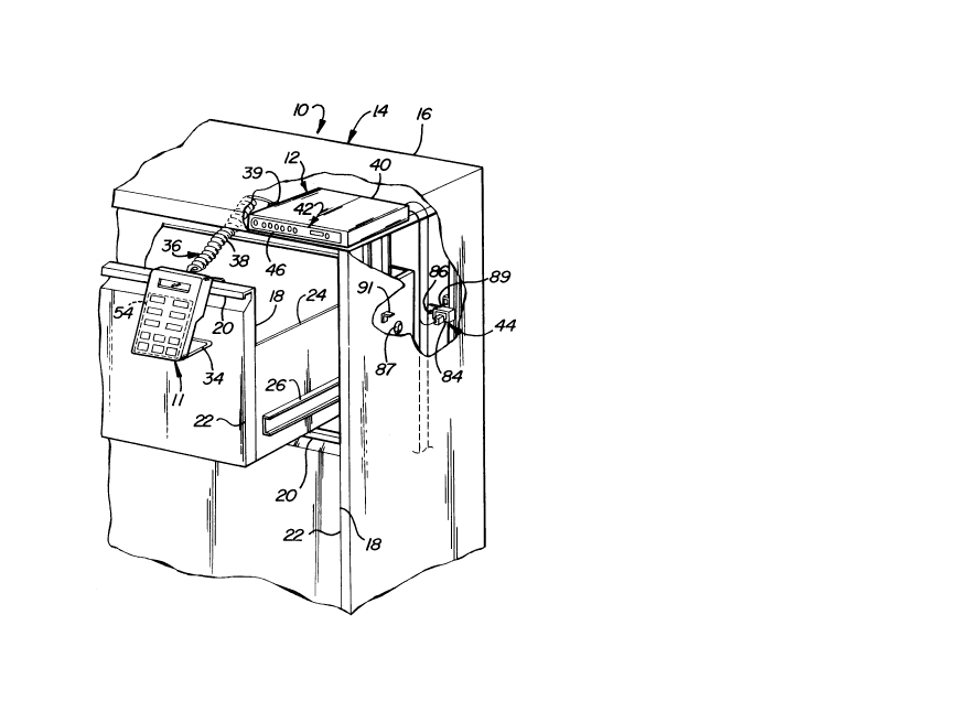
Referring to Figure 1, the subject
invention is generally shown at 10. The removable
programming means 11 is designed to interface with an
electronic lock, generally shown at 12, of a storage
assembly 14. The subject invention 10 is an
affordable means for accessing the memory of the
electronic lock 12. The electronic lock 12 will be
discussed in greater detail subsequently.
The storage assembly, generally indicated
at 14, may be any type of furniture with the capacity
to store items. In Figure 1, the storage assembly 14
is shown to be a file cabinet. The file cabinet 14
includes a housing 16 which defines an enclosure.
The enclosure is subdivided by storage units 18
wherein each storage unit 18, two fully shown, is
moveable between a closed condition and an open
condition; both conditions are represented by the top
and bottom storage units 18, respectively. The
storage units 18 may have handles 20 to aid in the
opening of a storage unit 18 to its open condition.
The storage units 18 also comprise a front 22, two
side 24, bottom and back (neither shown) surfaces.
The two side surfaces 24 have guides 26 that follow
tracks (not shown) attached to the side surface of
the housing 16. The storage units 16 are numbered
from top to bottom in ascending order. For example,
the top storage unit 18 is referred to as "one", the
storage unit 18 second from the top will be referred
to as "two", etc, the significance of which will be
discussed subsequently.
Meridian P-306 -6- Z0~5~96
The removable programming means 11 is seen
clipped to the handle 20 of the storage unit 18 in
the open condition in Figure 1. A clip 32 is U-
shaped to fit around the top of the front surface 22,
thus allowing the operator the freedom of not having
to hold the removeable programming means 10 while
operating it.
The removable programming means 11 further
includes retractable stand means 34 for positioning
the removable programming means 10 away from the
front surface 22 of the storage unit 18 to aid in the
operation thereof. The retractable stand means 34 is
a U-shaped piece of hard material, typically metal,
with hinges (not shown) attaching the retractable
stand means 34 to the back of the subject invention
for allowing rotation of the retractable stand
means 34 out of the way to facilitate storage when
the removable programming means 11 is not being used.
The removable programming means 11 further
comprises a connection means, generally indicated at
36, for electronically connecting the removable
programming means 11 to the electronic lock means 12.
The connect means 36 comprises a long set of
conductive wires 38 insulated from each other so each
wire may act as a medium for the transmission of
separate and distinct electrical signals. The long
set of conductive wires 38 has a connection end 39
and is shown to resemble a standard long telephone
cord 38 because it is inexpensive, readily available
in the market place, and, most importantly, it is
designed to perform exactly the same task as the long
set of conductive wires 38. Of course, any type of
medium of transmission may be used in place of the
Meridian P-306 - 7 -
20~1D9~
telephone cord 38 without adding anything inventive
to the subject invention. Such substitutes may be
systems utilizing acoustics, optics or radio waves.
The electronic lock 12 is shown in Figure 1
to have control means 40, input means 42, and
individual locking means 44 (two shown). The input
means 42 is an alphanumeric keyboard 42. A
connection port 46 is placed adjacent the alpha-
numeric keyboard 42 and receives the connection end
39 of the long telephone cord 38. The connection
port 46 transmits all information transmitted through
the long telephone cord 38 by the removable
programming means 10 to the control means 40. The
electronic lock 12 will be discussed in more detail
subsequently.
The removable programming means 11 may be
seen in greater detail in Figure 2. The removable
programming means 11 is substantially rectangular in
shape. The removable programming means 11 has a face
side 48 subdivided into three (3) sections 50, 52,
54. The first section 50 is a flat empty space
suitable for printed material thereon. The second
section 52 is the area where the display exists. The
display 52 is a standard liquid crystal display
(LCD). Although the removable programming means 11
is designed to use LCD display #LM16255 produced by
Sharp Incorporated, any suitable display may be
used. The third section 54 of the subject invention
10 is a keyboard 54. The keyboard 54 comprises two
different and distinct types of keys; the mode keys,
generally indicated at 56, and the numerical keys 58.
The mode keys 56 are six keys, each individually
labelled "PROGRAM" 60, "PROGRAM VERIFY" 62, "NEXT" 64,
"DELETE" 66, "YES" 68 and "NO" 70. The mode keys
A
Meridian P-306 -8- Z 0 ~ 09
56 determine what information is to be manipulated
and how it is to be manipulated. The exact
operations each mode key 56 performs when the
operation of the subject invention 10 is discussed.
The numerical keys 58 consists of a 2 X 3
matrix of keys numbered by one (1) through six (6).
The three functions of the numerical keys 58 are: (i)
to input a security code to gain access to the
control means 40; (ii) to alter the status of access
codes by adding, deleting, or modifying the list of
access codes stored by the control means 40; (iii) to
input the storage units 18 that may be accessed by
inputting the particular access code.
Turning to Figure 3, the removable
programming unit 11 and the control means 40 are
shown in block diagram form. Additionally, the
blocks representing the power supply 72 and voltage
regulator 74 are shown.
The power supply 72 receives power from
line 76 carrying current in one of two possible
manners; a connection directly to a standard wall
outlet or a connection from a dedicated power line
wherein the dedicated power line is a part of wire
harness used when more than one or a bank of file
cabinets 14 are located in close proximity to one
another. The power supply 72 supplies 12 volts DC
along lines 78, 80 to the voltage regulator 74 and
the solenoid drivers 82. The voltage regulato~ 74
supplies the remaining control means with 5 volts DC
of electrical power. The solenoid driver 82 operates
the individual locking means 44 which comprises
individual solenoids 84, best seen in Figure 1. The
individual locking means 44, one pair associated with
each storage unit 18, have a normally locked
Meridian P-306 -9- Z055096
condition with the plunger 86 extended outwardly for
independently locking each of the storage units 18 in
the closed position and moveable to an unlocked
condition with the plunger 86 retracted inwardly
(seen in the storage unit 18 second from the top in
Figure 1) for independently allowing each of the
plurality of storage units 18 to the open position.
The control means 40 further comprises a
microprocessor 88. The microprocessor 88 is an 8-bit
CMOS microcontroller and operates per the
instructions, i.e. microcode, it receives from an
external electronically programmable read only memory
chip (EPROM) go. The microprocessor 88 stores and
retrieves the access codes and the storage units 18
assigned to that particular access code (hereinafter
"combined code") in an external CMOS memory chip 92.
The microprocessor 88 also compares the access codes
and/or security code, depending on the current mode
of operation, which are input via the keyboard 54 of
the removable programming means 11 or by the input
means 42 to the access codes and/or security code(s)
in the CMOS memory chip 92. The CMOS memory chip 92
comprises 200 registers (not shown) which
individually store each combined code therein and at
least one register for a security code. The
microprocessor 88 also controls four additional 8-bit
input ports, they being the key port matrix 94 of the
input means 42, the switch inputs 96, the buried code
jumpers 98 and the loop address 100. When any of
these four additional input ports 94, 96, 98, 100 are
enabled, the information stored therein is placed on
the 8-bit data bus 102 and sent to the microprocessor
88.
Meridian P-306 -10- 20~5096
The low order 8-bit address bus is
demultiplexed from the data bus with an 8-bit latch
104. This latch 104 stores the portion of the
instruction cycle on the falling edge of the address
latch enable control signal. This latched address is
delivered to the EPROM chip 90 and the CMOS chip 92.
The high order address bus 105 is output directly
from the microprocessor 88 and delivered to the EPROM
chip 90, the CMOS chip 92, and the address decode
circuitry 106.
The address decode circuitry 106 decodes a
high order address along with the data read control
signal 110 from the microprocessor 88 and delivers a
dedicated read signal 112 to each of the four 8-bit
input ports 94, 96, 98, 100. A dedicated read signal
112 is also delivered to the reset generation
circuitry 114 to continually interrupt the reset
generation circuitry and prevent the resetting of the
control means 40 during normal operation. The reset
generation circuitry 114 resets all of the circuitry
when a fault is detected.
The reset generation circuitry 114 will
hold the control means 40 in reset condition during
control means 40 power up and also disables the
control means 40, with a reset, if the input voltage
falls below a predetermined level. This prevents
erroneous data from being written into the CMOS chip
92 during system power up and down. The reset
generation circuitry 114 also contains a watchdog
timer (not shown). If for some reason the
microprocessor 88 program loses its place, the read
signal will not occur during a regular interval and
the watchdog timer will reset the system to normal
205~096
~- 11 68086-465
operation. The reset generation circuitry 114 also performs the
battery back-up function for the CMOS chip 92.
The control means 40 interfaces the removable
programming means 11 via the connection means 36.
A block diagram of the electronic circuit of the
removable programming means 11 is shown in Figure 4. A remote
voltage regulator 116 receives power from the long telephone cord
36 and supplies five volts DC to the rest of the removable
programming means 10. The access control interface 118 is also in
electrical communication with the control Deans 40 via the long
telephone cord 36. The access control interface 118 receives from
and transmits to the control means 40 information in relation to
the programming of the control means 40.
The access control interface 114 is in two-way
communication with the microprocessor 120 of the removable
programming means 11. The microprocessor 120 operates pursuant to
the request made through the key pad matrix 121, which contains
the mode 56 and numerical 58 keys, and the instruction it receives
from the EPROM chip 122 located in the removable programming means
11. In addition, the microprocessor 120 operates the BPROM chip
122 using control signals in conjunction with the high order
address bits. The microprocessor 120 also operates the display
decoder 124 which, in turn,
~-A
Meridian P-306 -12- 20~5~96
operates the display module 126. The display decoder
124 decodes the address range in which the display
data can be written. This decoder 126 inputs high
order address and data write signals from the
microprocessor 120 and generates a display write
signal which is interpreted by the display module
126.
Turning to Figure 5, a flow chart of the
operations of the microprocessor 120 of the subject
invention 10 is shown. When viewing the flow chart,
connecting path numerals always connect with the
highest like numeral on the page. For example,
numeral 1 at 128 is connected to numeral 1 at 130,
and not numeral 1 at 132. In addition, it is to
understood that, if at any point, the time taken to
input a complete code or response is greater than a
predetermined time, the microprocessor 120 will
immediately default to the default position 134 and
the operator will have to re-input the security code.
The removable programming means 10 is
turned on when, after it is plugged into the
connection means 36, the nPROGRAM" key 60 is pressed.
The microprocessor 120 is in the security mode and
any code input via the numerical keys 58 will be
checked against all acceptable security codes. If
the code does not match any of the storage security
codes, the removable programming means 11 turns off
and waits for the "PROGRAM" key 60 to be pressed. If
the security code is correct, the removable
programming means 11 becomes functional and it is
able to access the control means microprocessor 88.
The microprocessor 120 is able to operate
in two different modes. The first mode, represented
by the left-most branch in the flow chart in Figure
Meridian P-306 -13-
ZO~O9~
5, beginning at branch point 136, adds additional
access codes to the CMOS memory chip 92 given the
total number of access codes does not exceed 200. If
an existing access code is input, the removable
programming means 11 is considered in the "MODIFY"
mode wherein a new drawer assignment will be
associated with the existing access code. An access
code, when input into the electronic lock 12 of the
storage assembly 14 allows selective access to the
storage assembly 18. If the microprocessor 120 is
signalled by the depression of the "YES" key 68
representing the access code has been properly
entered, the microprocessor 120 receives the signals
of the numerical keys 58 which are pressed
representing the storage units 18 that may be opened
when the access code is used. When the
microprocessor 120 receives the signal from the "YES"
key 68, signalling the completion of data entry, the
microprocessor 120 sends all information, i.e., the
new access code and the associate storage units 18
that may be accessed, to the control interface 118
where it will be sent to the control means
microprocessor 88. The microprocessor 120 will
display the new access code and accessible storage
unit 18 numbers by sending a signal to display
decoder 124 which will operate the display module
126. If a signal from the "PROGRAM" key 60 is
received, the microprocessor 120 will return to
branch point 136. If not, the removable programming
means 10 will automatically return to default
position 134.
The second mode of operation, represented
by the right-most branch, beginning at branch point
136, in Figure 5, is the verification mode. The
-
Meridian P-306 -14- Z05~09~
microprocessor 120 automatically enters the
verification mode when the "PROGRAM VERIFY" key 62 is
pressed. The microprocessor 120 immediately sets a
register counter X, as may be seen in block 138, to
zero (0). The microprocessor 120 increments the
value of X and checks the value of X (now one). If
the value of X equals one more than the number of
stored access codes, the microprocessor 120 returns
to the branch point 136. If X is less than the
number of stored access codes, the microprocessor 120
will direct the access code in register X to be
displayed. The microprocessor always "knows" how
many access codes are stored. If only 10 access
codes are stored, only 10 access codes can be
displayed (not 200). If the "DELETE" key 66 is
pressed, the microprocessor 120 will send a signal to
the control means microprocessor 88 to delete the
access code and register X only after the nYES" key
68 has been pressed reaffirming the deletion. The
NNEXT" key 64 may be sequentially pressed to scroll
through all the registers by incrementing X and
deleting those not needed.
A computer 115 may be in permanent
communication with the control means 40. The
computer 115 can perform all of the above-mentioned
operations the removable programming means 11 may
perform. The computer 115 is capable of deleting
blocks of combined codes at a time. In addition, the
computer may perform logging operations for logging
which access codes have been used or attempted to be
used.
Meridian P-306 -15- 2055096
A more detailed schematic of the circuitry,
generally shown at 140, is shown in Figure 6. In
general, the downwardly pointed triangles are all
connected to ground.
Vcc is 5 volts DC and is produced by the
power regulator 142, an LM7805 power regulator, and
powers the whole circuit 140. The power regulator
142 receives 12 volts DC from the green wire 144 in
the long telephone cord 36. The capacitor C1 is
connected to ground and to the green wire 144 in
parallel with the power regulator 142 and decouples
the power as it is received by the circuit 130. The
capacitor C2, C3 and C4 decouple the three integrated
circuits 120, 122, 176, discussed in greater detail
subsequently. The capacitor C2, C3, C4 are in
parallel to each other and are connected between the
output of the power regulator 142 and ground.
Although not shown in the circuit 140, the capacitor
C2, C3, C4 are placed in close proximity in their
respective integrated circuits 120, 122, 176.
The black 150 and white 152 wires are
used as grounds while the red wire 154 of the long
telephone cord 38 is used to signal the control means
that the removable programming means 10 is
present.
The remaining two lines, the yellow wire
156 and the blue wire 158 are indirectly connected to
the microprocessor 120. Generally, the yellow wire
156 carries information from the removably
programming means 10 to the control means 40 of the
electronic lock 12 while the blue wire 158 carries
information from the control means 40 to the
mlcroprocessor 120.
Meridian P-306 -16- 20S~096
More specifically, the microprocessor 120
directs two transistors Ql, Q2 when communicating
with the control means 40. The transistor Ql is an
open collector driver transistor wherein the
collector is connected directly to the yellow wire
156, the emitter is connected directly to the ground,
and the base is connected to a resistor Rl. The
resistor Rl is connected in parallel to the
microprocessor 120 and a resister R2. The resistor
R2 is connected in parallel to the resistor R1 and
the microprocessor 120. The resistor R2 is also
connected to Vcc. The transistor Ql transmits serial
data to the access control interface 118. The
resistor R2 is used to assist the sourcing
capabilites of the output.
The microprocessor 120 is also connected in
parallel to the transistor Q2 and to the resistor R3.
The resistor R3 is also connected to Vcc. The
collector of the transistor Q2 is connected to the
microprocessor 120. The emitter of the transistor Q2
is connected to ground while the base is connected to
two resistors R4, R5 which are parallel to each
other. The resistor R5 is connected to ground and
the resistor R4. The resistor R4 is connected to the
diode Dl. The diode Dl is removably connected to the
blue wire 158 and to the resistor R6. The resistor
R6 is also connected to Vcc. The transistor Q2 is
used as a serial input buffer. The open collector
serial drive will transmit data by "sinking" current
through the resistor R6. This will pull the anode of
diode Dl low. Because of the noise induced by and
the resistive nature of the long telephone cord 38
between the access control interface 118 and the
removeable programming means 10, this load cannot be
20~096
Meridian P-306 -17-
guaranteed to be a logic 0. The diode Dl is used to
add a threshold voltage to the base emitter junction
of the transistor Q2. Now any serial input signal
less than 1.4 volts will be recognizes as a logic 0
and will, therefore, turn off the transistor Q2. The
resistor R3 is the base bias resistor for the
transistor Q2 and the resistor R5 is used to ensure
the turn off of the transistor Q2 when the diode Dl
stops conducting with the low level input signal.
The microprocessor 120 is an INTEL number
80C31 microprocessor and it is used with an external
EPROM chip 122 for program storage. This design was
chosen to allow an easy software update. The
microprocessor 120 has three ports; the first port
162 is port 0, the second 164 is port 1 and the third
port 166 is port 2. The first port 162 interfaces
both the display module 126 and the EPROM chip 122.
The second port 164 interfaces the keyboard 54 and
third port 166 interfaces the EPROM chip 122. The
first port 162 is the address/data bus on the
microprocessor 120. The address bits 0-7 appear on
this bus on the first half of the bus cycle and are
latched on the falling edge of the address latch
enable clock 168. The EPROM chip 122 contains an
address latch internal to itself. After the address
latch enable 168 signal goes low, data bits 0-7
appear on the second half of the bus cycle. The bits
are either directed to the display module 126 during
a data write procedure or received from the EPROM
chip 122 during an instruction read process.
The third port 168 contains the high order
address bits 8-15. The bits 8-12 of this bus are
directed to the EPROM chip 122 for high order
_ Z055096
Meridian P-306 -18-
addressing. The bits 13 and 14 are used for display
module 126 control. All address latching is
performed inside the EPROM chip 122.
The microprocessor 120 utilizes an 11.00
MHz crystal 160 because this oscillation frequency
allows the microprocessor 120 to produce a 9600 BAUD
rate for serial communications. The capacitors C5,
C6 on either side of the crystal 160 are used to
produce the needed 11.00 MHz frequency.
The keyboard 54 is connected to the second
port 164 of the microprocessor 120. New access
codes, and modes of manipulation, i.e. deletion, are
sent to the microprocessor 120 via the second port
164. Bits 0-3 are used as row outputs and bits 4-6
are used as column inputs. Row outputs bits 0-3 are
driven low and then high, sequentially. After each
row output is driven low, column input bits 4-6 are
read. If a key is pressed, a column input will be
read as a logic low. The column number that is read
and the row that is presently driven low will be
recorded and compared to a look up table. The value
of the pressed key can now be determined by using row
and column values as pointers to this look up table.
The diodes D2, D3, D4, D5 are used to
isolate row outputs from each other in the event that
more than one key 56, 58 is pressed on the keyboard
54. The resistors R6, R7, R8 are connected in
parallel between Vcc and the bit connections 5-7.
The first port 162, identified as port 0 by
Intel, interfaces with both the display module 126
and the EPROM chip 122. The first port 162 data bits
0-7 drive the diplay data bus directly. The display
module 126 is permanently placed into the write mode
by tying its write enable line 170 low. A display
Meridian P-306 -19-
2055096
pin 172 is the control/data selection signal and the
state of this line determines the function of the
data written to the display module. A logic 0 on
this pin 172 will cause the data to be written into
the display control register (not shown) and a logic
one on this pin 172 will cause the data to be
written to the display data buffer (not shown).
The display enable pin 174 is used to write
data onto the display 52. The NAND integrated
circuit, generally shown at 176, is used to decode
the write signal. The NAND IC 176 is used to "AND"
the inverted microprocessor 120 write signal with the
address bit 172. Therefore, the display 52 will
write only when the address bit is set to logic 1.
The value at the WR pin 175 of the microprocessor 120
is NANDed with itself using NAND gate 184. The
seventh bit of the third port 166 is NANDed with the
output of the first NAND gate 184 using NAND gate
186. This output is NANDed with itself using NAND
gate 188 where it is tied to the display enable pin
174.
The adjustment pin 178 adjusts the contrast
of the display 52. The adjustment pin 178 is
hardwired to two resistors Rg, R1o wherein Rg is
connected between ground and pin 1 of the display
module 126. The resistor R8 is connected between the
adjustment pin 178 and both the second pin of the
display 126 and Vcc. The values for the resistors
Rg, R1o are chosen because its values are suitable
for many display modules similar to that of the
display module 126. In particular, these values work
well with the display module 126 produced by SHARP.
Meridian P-306 -20- 20S5096
Vcc is also connected in parallel, through
eight resistorS Rll, R12~ R13~ R14~ Rls~ R16' 17'
R18, with the display module 126, the zero port 180
of the EPROM chip 122, the A port 182 of the EPROM
chip 122, and the first port 162 of the
microprocessor 120.
In operation, the method of changing the
access code of an electronic lock 12 for a storage
assembly 14 having a plurality of storage units 18
and removable programming unit 10 would comprise the
steps of: connecting the removable programming unit
10 to the storage assembly 14 via connection end 3g
and connection port 46; entering the programming mode
of operation by pressing any one of the mode keys 56
and altering the status of the plurality of access
codes by entering the access code or numerals
representing particular storage units 18 via the
numerical keys 58. This method is characterized by
removing the removable programming unit 10 from the
proximity of the storage assembly 14 after completing
operations. This may be done by removing the
connection end 39 from the connection port 46 thus
severing the mode of communication. This prevents
any unauthorized alteration of status of the
plurality of access codes which may be done
inadvertently if the programming capability of the
removable programming unit 10 were constantly present
and in communication with the microprocessor 120 of
the subject invention 10.
More particularly, the method of operation,
shown in Figure 7, begins with the operator
connecting the long telephone cord 38 of the subject
invention 10 to the control means 40 of the
electronic lock 12 via the connection port 46. The
Meridian P-306 -21- 20550~6
nPROGRAM" key 60 is pressed to prepare the subject
invention 10 to send the security code to the control
means 40. 'ENTER SECURITY CODE' will appear on the
display 52. If the security code is valid, 'ENTER
SECURITY CODE' will appear and the operator will
either add a new code or verify/delete an existing
code. If the security code is incorrect, 'WRONG CODE
TRY AGAIN' will appear on the display 52 and the
operator must repress the "PROGRAM" key 60 and try
again.
If a new access code is being added, it
must be input at this point. Immediately following
the new access code, the storage unit 18 numbers are
to be inserted delineated by pressing the "YES" key
68. The display 52 will verify the new access code.
To modify the storage units 18 that may be
accessed using an existing access code, the operator
must input the existing access code as if it were a
new access code. The storage units 18 may then be
added in the same fashion as the storage units 18 for
a new access code are entered, discussed above. In
other words, the new assignment of storage units 18
will overwrite the old assignment of storage units
18.
If the operator wishes to verify or delete
the code, the "PROGRAM VERIFY" key 62 must be
pressed. The first access code i.e. the access code
stored in register number 1 will be displayed. The
"NEXT" key 64 may be repeatedly pressed until the
desired code is reached. The "DELETE" key 66 is
pressed followed by the "YES" key 68, as verification
and the instruction to delete the access code is sent
to the control means 40 where the access code is
Meridian P-306 -22- ZOS509~
deleted from the control means CMOS memory chip 92.
To continue through the list of access codes, the
operator must begin pressing the "NEXT" key 64 again.
When no more access codes exist, the message 'NO MORE
ACCESS CODE ENTRIES' will appear in the display 52.
At any time throughout this method, the
operator may redirect his search or mode of operation
by pressing the "PROGRAM" key 60.
The invention has been described in an
illustrative manner, and it is to be understood that
the terminology which has been used is intended to be
in the nature of words of description rather than of
limitation.
Obviously, many modifications and
variations of the present invention are possible in
light of the above teachings. It is, therefore, to
be understood that within the scope of the appended
claims wherein reference numerals are merely for
convenience and are not to be in any way limiting,
the invention may be practiced otherwise than as
specifically described.