Note: Descriptions are shown in the official language in which they were submitted.
.
- NULTI-C~N~T DIGITAh RECEIVER
FOR GLOBAL PO8ITIONING 8Y8TEM 2~551~5
FIELD OF THE INVENTION
This invention relates generally to digital radios which
receive pseudorandom noise (PRN) encoded signals such as those
used in navigation systems.
BAC~GROUND OF THE INVENTION
Passive pseudorandom noise (PRN) ranging systems such as
the United States' Global Positioning System (GPS) and the
Union of Socialist Republics' Global Navigation System
(GLONASS) allow precise determination of latitude, longitude,
elevation and time. A PRN ranging system receiver
accomplishes this by using time difference of arrival and
Doppler measurement techniques on precisely-timed signals
transmitted by orbiting satellites. Because only the
satellites transmit, the need for two-way communications is
avoided, and an infinite number of receivers may be served
simultaneously.
However, the transmitted signal must contain a number of
components in order for the receivers to extract the requisite
information; Thus each satellite transmits on at least one
carrier frequencies. Each carrier is modulated with low
frequency (typically 50Hz) digital data which consists of
information such as the satellite's ephemeris, (i.e.
position), current time of day, and system status information.
The carrier is further modulated with one or more high
frequency unique pseudorandom noise (PRN) codes.
A PRN receiver thus receives a composite signal
consisting of one or more of the signals transmitted by the
satellites within view, that is within a direct line-of-sight,
as well as noise and any interfering signals. Because the
2055~ 05
signals transmitted by different satellites use unique PRN
codes or unique frequencies, the receiver may separate the
signals from different satellites using code-division multiple
access (CDMA) or frequency division multiple access (FDMA)
techniques. The PRN codes also provide a mechanism to
precisely determine the signal transmission time from each
satellite. By determining the transmission time from at least
four satellites, and knowing each satellite's ephemeris and
approximate time of day information, the receiver's three
~ime~ional position, velocity and precise time of day can be
calculated.
For more information on the format of the GPS CDMA
system signals, see "Interface Control Document ICD-GPS-200,
September 26, 1984", published by Rockwell International
Corporation, Satellite Systems Division, Downey, California
90241.
For more information on the format of the GLONASS
system signals, see "The GLONASS System Technical
Characteristics and Performance", Working Paper, Special
Committee on Future Air Navigation Systems (FANS),
International Civil Aviation Organization (ICAO), Fourth
Meeting, Montreal, Quebec, Canada, 2-20 May 1988.
A number of difficulties exist with present-day PRN
receivers. One such problem concerns accurate tracking of the
received composite signal. Another is determining and
correcting carrier phase lock loop cycle slipping. Another is
determining and correcting ionospheric divergence. The typical
PRN receiver includes a downconverter and a mixer. At the
downconverter, the input radio frequency (RF) signal from the
antenna is amplified, filtered, and downconverted to an IF
frequency by mixing it with a locally generated carrier
reference signal. The decoder, typically consisting of a mixer
ZQ~ 5
-3-
positioned either before or after the downconverter multiplies
the incoming signal with a locally generated PRN code reference
signal. If the locally generated PRN code is properly
correlated with that of the incoming signal, the digital data
results.
In either implementation, however, the circuits required
to perform the frequency and phase discrimination necessary to
accurately generate the local carrier and PRN code reference
signals are complex and costly, mainly because the composite
signal ideally has a power level of 16 decibels (dB) below
thermal noise. These circuits may also introduce errors due to
component mismatches when the signals from several satellites
are processed to calculate the receiver's position.
In addition, given the low level of received composite
signal, CDMA receivers are typically quite susceptible to
corruption by interfering continuous wave (CW) signals.
For high accuracy applications, atmospheric distortion
of the transmitted signals must also be corrected. The
principal source of such distortion is the ionosphere, which
manifests itself as a delay of the PRN code phase and advance
of the carrier phase. Since the amount of ionospheric
distortion is a function of the carrier frequency and the total
electron count along the path of the signal, the discrepancy in
delay between two signals transmitted at different carrier
frequencies from a single satellite may be used to determine an
absolute correction factor. However, this absolute divergence
correction requires twice the hardware to demodulate and decode
both frequencies simultaneously. Furthermore, in some systems,
such as GPS, access to the PRN code on the second frequency is
limited. In certain systems, a relative divergence between the
two frequencies can be determined by tracking the phase
difference in carrier frequencies, without first decoding the
-4- ~ 5
second carrier, by simply squaring the received carrier
signal. However, either approach requires radio frequency (RF)
circuitry which at least partially processes two RF signals.
SUMMARY OF THE INVENTION
Briefly, the invention is a receiver for pseudorandom
noise (PRN) encoded signals consisting of a sampling circuit, a
carrier/code synchronizing circuit, and a digital correlator
with dynamically adjustable code delay spacing and selectable
delay modes.
The sampling circuit provides digital samples of a
received composite PRN signal at a rate which is much higher
than twice the PRN code chip rate. A receiver channel is
assigned to track the PRN signal from a particular transmitter;
each receiver channel includes a synchronizing circuit and two
di~ital correlators.
Bach synchronizing circuit is a numerically controlled
oscillator which provides a local carrier reference signal and
a local code reference signal which are synchronous with each
other. Together with the correlator outputs, the synchronizing
circuit also enables detection and correction of cycle slips in
the local carrier reference and detection of relative code and
carrier divergence.
The correlators correlate the digital samples of the
composite signal with the locally generated PRN code values to
produce a plurality of early, late, punctual, or early-minus-
late correlation signals. The correlation signals are
accumulated and processed to provide feedback signals to
control code and carrier synchronizing. Because both carrier
and code synchronizing are performed by the same circuit, a
_
-5- 2~5~5
relative diversion-type correction for ionospheric distortion
may be implemented by simultaneously detecting any code or
carrier divergence.
The sampling circuit output may also be fed to an
amplitude probability density function circuit which detects
the presence of interfering or jamming signals. When jamming
signals are detected, the sampling circuit amplitude thresholds
are adjusted to provide improved operation. The probability
density function circuit is also used to control an automatic
gain control amplifier.
The correlators may also be switched between a first, or
acquisition mode, and a second, or tracking mode. In the
acquisition mode, the correlators are set to give an early and
lat:e correlation power indication.
Once the proper carrier and phase are obtained, one of
the correlators is configured as punctual for optimal carrier
tracking, and the other correlator as early minus late with a
narrow time delay to provide optimum code tracking.
Certain functions of the synchronizing circuit and
correlators are preferably performed by a general purpose
computer and suitable software.
There are several advantages to this arrangement.
Because the system is nearly completely digital, and because a
common digital signal is fed to all receiver channels, the
in,vention reduces channel biasing errors and thus increases
position measurement accuracy. Furthermore, because only a
single common RF stage is required, the invention eliminates a
number of difficulties such as component matching associated
with other types of systems.
~ 2055~ o5
6~421-485
Because the samples are processed at a high rate, large
Doppler offsets may be corrected. This in turn enables a less
expensive analog local oscillator circuit to be used.
By synchronously controlling the local PRN code
generator and carrier phase lock circuit in a single numerically
controlled oscillator, pseudorange meaæurements having high
accuracy and low-noise result.
Since there is accurate tracking of the PRN code, cycle
slips of the carrier can be easily detected and corrected, and
real time differential measurements are significantly better.
Divergence between locally generated carrier and code
reference signals can be detected and thus a relative diversion
correction for ionospheric distortion is provided.
The probability density function detector enables
improved performance in the presence of jamming signals.
The dynamically configurable correlators provide fast
code and carrier acquisition while providing low noise signals
during steady-state tracking.
According to one broad aspect, the invention provides a
receiver for decoding a composite signal consisting of a plurality
of pseudorandom noise (PRN) encoded signals, the receiver
comprising: means for generating a local clock signal; a sampling
circuit, connected to receive the composite signal and the local
clock signal, and to provide digital in-phase tI) and quadrature
(Q) samples of the composite signal; a channel circuit, for
decoding one of the PRN encoded signals, wherein the channel
circuit further comprisesS means for generating a Doppler shift
estimate signal; a correlator, connected to receive the I and Q
samples, a local carrier reference signal, and a local code
reference signal, and to provide a code adjustment signal; and a
code and carrier synchronizing circuit, connected to receive the
sample clock signal, the Doppler shift estimate signal, and the
code adjustment signal, for providing the carrier reference signal
and the code reference signal, with the carrier reference signal
and code reference signals in synchronism with each other.
A 6
~ 2Q~5 ~ 05
64421-485
According to another broad aspect, the invention
provides a receiver for decoding a composite signal consisting of
a plurality of pseudorandom noise (PRN) encoded signals, the
receiver comprisingS means for generating a local clock signal; a
sampling circuit, connected to receive the composite signal and
the local clock signal, and to provide digital in-phase (I) and
quadrature (Q) samples of the composite signal; and a channel
circuit, for decoding one of the PRN encoded signals, wherein the
channel circuit further comprises: means for providing a local PRN
code signal; and a pair of correlators, each correlator connected
to receive the I and Q samples and the local PRN code, and to
provide a decoded signal, wherein the ~orrelators have dynamically
selectable delays.
According to a further broad aspect, the invention
provides a receiver for decoding a composite signal consisting of
a plurality of pseudorandom noise (PRN) encoded signals, the
receiver comprisingS means for generating a local clock signal; a
gain control ~ir~uit, conne~ted to receive the composite signal
and having a gain control input, and connected to provide a gain-
controlled composite signal; a sampling circuit, connected toreceive the gain-controlled composite signal and the local clock
signal, and to provide digital in-phase (I~ and quadrature (Q)
samples of the composite signal; a plurality of counters, with a
counter associated with a particular expected absolute value of
the digital I and Q samples, and the counters arranged to
increment each time an I or Q sample having the corresponding
magnitude is output by the sampling circuit; and means for reading
the values of the counters and adjusting the gain control input of
the gain control circuit.
B~IEF DESCRIPTION OF THE DRAWINGS
The above and further advantages of the invention may be
better understood by referring to the following description in
conjunction with the accompanying drawings, in which:
Fig. 1 is a block diagram of a PRN receiver constructed
in a~cordance with the invention, including a downconverter,
sampler, channel, and processor circuits;
, ~
6a
-7- ~ 5
Fig. 2 is a circuit diagram of the downconverter
circuit;
Fig. 3 is a circuit diagram of the sampler circuit;
Fig. 4 is a block diagram of the channel circuit;
Fig. 5 is a circuit diagram of a carrier/code
synchronizing circuit used in each channel circuit;
Fig. 6 is a timing diagram showing the relative duration
of various portions of a received PRN signal; and
Fig. 7 is a circuit diagram of a correlator circuit used
in each channel circuit.
DET~TT~T~n DESCRIPTION OF ILLUSTRATIVE EMBODIMENTS
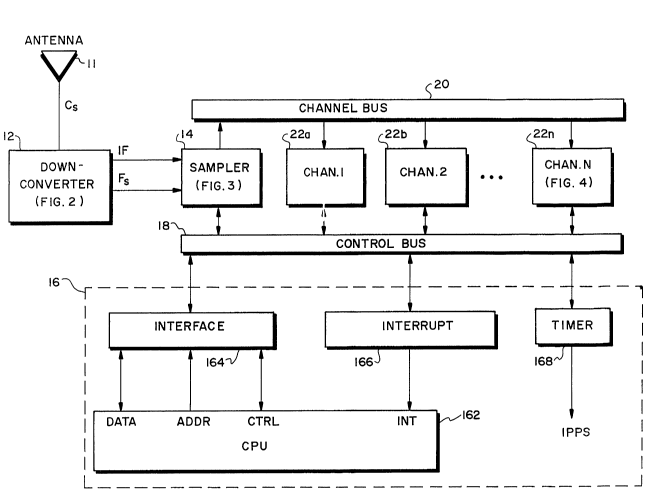
Fig. 1 is an overall block diagram of a pseudorandom
noise (PRN) ranging receiver 10 constructed in accordance with
the invention. It includes an antenna 11, downconverter 12,
sampler 14, processor 16, control bus 18, channel bus 20 and
multiple channels 22a, 22b, . . . , 22n, (collectively, the
channels 22). The illustrated receiver 10 will be primarily
described as operating within the United States' Global
Positioning System (GPS), however, adaptations to the Union of
Soviet Socialist Republics' GLONASS are also described.
The antenna 11 receives a composite signal Cg consisting
of the signals transmitted from all participating satellites
within view, that is, within a direct line of sight of the
antenna 11. For example, when the GPS system is fully
operational, with world-wide coverage, twenty-four satellites
will be in operation, and signals from as many as eleven GPS
-8- 2Q~ 5
satellites may be received simultaneously.
The composite signal C8 is forwarded to the
downconverter 12 to provide an intermediate frequency signal IF
and a sample clock signal F~. The IF signal is a downconverted
and filtered version of the composite signal Cs. The Fg signal
indicates the points in time at which samples of the IF signal
are to be taken. The downconverter 12 is discussed in greater
detail in connection with Fig. 2.
The sampler 14 receives the IF and F8 signals and
provides digital samples of the IF signal to the channels 22
via the channel bus 20. The samples consist of in-phase (I8)
and quadrature (Qs) amplitude samples of the IF signal taken at
the times indicated by the F8 signal. The sampler is detailed
in Fig. 3.
Each channel 22 is assigned to process the signal
transmitted by one of the satellites presently within view of
the antenna 11. A given channel 22 thus processes the I8 and
Q~ signals and tracks the carrier and code of the signal
transmitted by a particular satellite. In particular, each
channel 22 uses a carrier/code synchronizing circuit to
frequency and phase-track the PRN encoded carrier signal by
maintaining an expected doppler offset unique to the desired
satellite. The channel 22 also correlates a locally generated
PRN code reference signal with a doppler-rotated replica of the
carrier. Two correlators, connected in a delay lock
arrangement, keep the locally generated PRN code precisely
aligned with the code modulated onto the received signal by the
satellite. The resulting decoded data, including the
sat:ellite's ephemeris, time of day, and status information, as
well as the locally generated PRN code phase and carrier phase
measurements, are provided to the processor 16 via the control
bus 18. The channels 22 are described in detail in connection
g ZQ~i5~)s
with Fig. 4.
The sampler 14 and channels 22 are controlled by the
processor 16 via the control bus 18. The processor 16 includes
a digital central processing unit (CPU) 162 which typically
supports both synchronous-type input/output (I/O) via a
multiple-bit data bus DATA, address bus ADDR, and control
signals CTRL and synchronous controller circuit 164, as well as
an interrupt-type I/0 via the interrupt signals, INT and an
interrupt controller circuit 166. A timer 168 provides certain
timing signals such as the measurement triggers MEAS and a
time-stamp signal lPPS, as will be described. The operation of
the processor 16 and its various functions implemented in
software will be better understood from the following
discussion.
Referring now to Fig. 2, the downconverter 12 includes
an RF bandpass filter 120, low noise amplifier 121, mixer 122,
intermediate-frequency filter 123, and final amplifier 124. A
local reference oscillator 125 provides a samples clock signal,
F~. A voltage controlled oscillator (VCO) 131 is phase locked
to the reference oscillator 125 by using a synthesizer 132 and
fi]ter 133 arranged in a feedback loop. The VC0 131 provides a
local osicallator reference signal, LO, to the mixer 122.
The composite signal C~ received from the antenna 11
typically consists of PRN modulated signals from all satellites
within view (that is, within a direct line-of-sight of the
receiver 10), any interfering signals, and noise. Of interest
are the PRN modulated L-band carrier frequencies, some typical
L-band signals used by various ranging systems are as follows:
-lo- 2055~5
SPECIFICATIONS FOR CERTAIN PRN RANGING SYSTEM SIGNALS
L-Band Carrier Frequency PRN Code Rate Power
GPS L1 C/A 1.57542 GHz 1.023 MHz -160 dBW
GPS L1 P 1.57542 GHz10.23 MHz -163 dBW
GPS L2 1.22760 GHz10.23 MHz -166 dBW
GLONASS C/A 1.602.. 1.616 GHz 511 KHz
GLONASS P 1.602.. 1.616 GHz 5.11 MHz
Natural background noise at about -204 dBW/Hz is typically
mixed in with the L-band signals as well.
The Cg signal is first fed to the RF bandpass filter 120
which is a low insertion-loss filter having a bandpass at the
desired carrier frequency. The bandpass filter 120 should be
sufficiently wide to allow several harmonics of the PRN code to
pass. In the preferred embodiment for GPS L1 C/A signal
reception, this bandwidth is at least 10 MHz. After passing
through the low-noise pre-amplifier 121, the mixer 122
downconverts the received signal from the carrier frequency to
a desired intermediate frequency that is within the frequency
range of the sampler 14. The intermediate frequency filter 123
is also a bandpass filter having a sufficiently narrow
bandwidth to remove any undesired signals, but sufficiently
wide to keep the desired 10 MHz bandwidth. The final amplifier
124 is used as a pre-amplification stage to provide the output
IF signal with appropriate amplification. Although the
illustrated downconverter 12 is a single-stage downconverter,
there could, of course, be additional intermediate stages
used.
The reference oscillator 125 provides a stable digital
frequency local reference signal Fg to the synthesizer 132 as
ZQ~5~ ~5
well as the sampler 14. The VCO 131 provides the reference
signal LO to the synthesizer 132. The synthesizer 132
frequency-divides the L0 signal by a predetermined number and
mi~:es it with the reference signal Fg. The output of the
synthesizer 132 is then fed to the loop filter 133 to develop a
voltage which in turn controls the VC0 131.
Fig. 3 is a detailed diagram of the sampler 14, including
an automatic gain control (AGC) amplifier 140, digital-to-
analog (D/A) converter 141, A/D converter 143, two-bit counter
144, sample translator 145, and probability density function
(PDF) counters 146a, 146b, and 146c (collectively, the PDF
counters 146).
The sampler 14 receives the IF and the F~ signals from
the downconverter 12 and provides digital sampled signals I8
and Q~ to the channels 22 via the channel bus 20. The sampler
14, together with the processor 16 via the control bus 18, also
performs automatic gain control (AGC) and jamming suppression
functions.
More particularly, the intermediate frequency signal IF
is first fed to the AGC amp 140 which provides an amount of
amplification set by the processor 16 via the control bus 18
and D/A 141. The output signal from the AGC amp 140 is sent to
the analog-to-digital-converter 143.
The A/D converter 143 samples at precisely 90 phase
rotations of the IF signal's carrier frequency, as specified by
the F5 signal. Since successive in-phase samples Is and
quadrature samples Qg are required, the frequency of the
digital sample clock F~ must be equal to 4 IF/J, where J is any
odd integer. The Nyquist sampling theorem also dictates that
the sample rate be at least twice the bandwidth of the IF
signal. With the digital sample clock F~ chosen according to
-12- 2Q~
these guidelines, the output samples from the A/D 143 are thus
in in-phase and quadrature order as i,q, -i, -q, i,q . . .
The F~ signal also drives a two-bit counter 144 which is
used by the sample translator 145 to separate the samples
output by the A/D 143 into the sample signals Ig and Qg. The
most significant bit, SIGN, of the counter 144 is used by the
sample translator 145 to reverse the sign on the -i and -q
samples. The least significant bit of the counter 144
represents the IORQ signal that is used by the channels 22 to
identify individual samples on the I~, Qg bus as either an i or
a q sample.
If the A/D converter 143 is a three-bit device, the
out:put samples have two magnitude bits and a sign bit. Each
sample will thus be either a +/-1, +/-2, or +/-3.
The sample signals I~ and Q8, along with the IORQ and F~
signals, are routed to the sample bus 20 to be processed by the
channels 22.
The samples output from the A/D converter 143 are also
used to develop an estimate of the probability density function
for the amplitude of the incoming IF signal. This estimate is
used by the processor 16 to provide a gain control signal GAIN,
which is fed through the D/A converter 141 to control the gain
of the AGC amp 140. The probability density function estimate
is obtained by clocking one of the appropriate PDF counters
146a, 146b, or 146c according to the absolute value of each
sample. For example, magnitude +2 and magnitude -2 samples
cause the PDF2 counter 146b to be incremented. The PDF1
counter 146a and PDF3 counter 146c are similarly clocked each
time a sample with the corresponding magnitude is received.
When any one of the PDF counters 146 reaches a terminal count,
a CARRY signal is asserted and the DISABLE inputs are set so
-13- 2~ 5
that all PDF counters 146 stop counting. The contents of the
PDF counters 146 can be read and reset by the processor 16 via
the control bus 18.
To set the AGC level, the processor 16 periodically reads
the values of the PDF counters 146 and then resets them so that
another PDF measurement may begin. The processor 16 then
compares the measured signal amplitude distribution data with
the expected distribution of the sample amplitudes. Since the
expected probability density function is Gaussian, 49% of the
samples are expected in PDFl counter 146a, 32% in PDF2 counter
146b, and 19% of the samples in PDF3 counter 146c. If this is
indeed the approximate result, then the AGC 140 is properly
set. However, if too many samples are counted by the PDFl
counter 146a, for example, then the GAIN signal is set too low.
Similarly, if too many samples are counted by the PDF2 counter
146c, the GAIN signal is set too high. The processor 16, if
necessary, then loads a corrected gain control value into the
D/~ 141 via the control bus 18, which in turn adjusts the gain
of the AGC 140. This process continues periodically to
maintain the GAIN level such that the PDF1 count remains at
49~.
The processor also checks PDF counters 146b and 146c to
de1:ermine if they are close to the expected 32% and 19%. If
there is a continuous-wave (CW) interference present, the PDF3
colmter 146c will drop towards 0% and the PDF2 counter 146b
will increase towards 51%, depending on the level of the
in~erfering signal.
If the processor 16 detects this condition, it enters a
CW anti-jamming mode. In a CW anti-jamming mode, the processor
16 adjusts the D/A 141 such that the count in PDFl 146a is
maintained at 85%. It also expects to detect 15% of the
samples in the PDF2 counter 146b, and no samples in the PDF3
-
-14- 20~ S
counter 146c. In this mode, the processor 16 also enables the
JAMMED control line so that the translator 145 will rescale the
samples output by the A/D 143. In particular, samples of
amplitude +/-1,+/-2,+/-3 are mapped into amplitudes 0,+/-1,0,
respectively. The AGC 140 is also set so that the peak
positive and negative voltages of the CW signal correspond to
the +1/+2 and -1/-2 threshold levels of the A/D 143, so that
the thresholding logic of the A/D 143 directly demodulates the
de~;ired signal and rejects the jamming signal. With anti-
jamming mode enabled, an approximate improvement of 12dB has
been observed over purely analog receives, and 25dB improvement
over 1 bit hard- limited digital receives.
A truth table for the translator 145 is given by the
fo]lowing:
Is or Q5 (Per IORQ)
Input from SIGN=0 SIGN=1 SIGN=0 SIGN=1 PDM Counter
A/D JAMMED=0 JAMMED=1JAMMED=0 JAMMED=l Incremented
3 3 -3 0 0 pdf3
2 2 -2 1 --1 pdf2
-1 0 0 pdfl
-1 --1 1 0 0 pdfl
-2 -2 2 -1 1 pdf2
-3 --3 3 0 0 pdf3
Turning now to Fig. 4, a typical channel 22n is shown.
The channel 22n includes a carrier/code synchronizer circuit
220, PRN code generator 230, two correlators 240a and 240b
(collectively, correlators 240), a delay line formed by the
flip-flops 250 and 251, XOR gate 255, and switch 256. The
channel 22n tracks the PRN encoded signal transmitted by a
particular satellite from the Ig and Qs samples of the
composite, signal by correlating them with a locally generated
replica of the appropriate PRN code. It also rotates the Is
and Q5 samples to remove any Doppler frequency offset caused by
=
-15- 2~ 5
satellite motion, receiver motion, and reference oscillator
errors.
Briefly, the synchronizer 220 is a single numerically
controlled oscillator (NCO) which uses the sample clock Fg and
appropriate instructions from the processor 16 to provide the
control signals required by PRN code generator 230 and
correlators 240 to track the frequency and phase of the
carrier, including any residual Doppler, as well as to track
the PRN code.
The code generator 230 uses signal pulses output by the
synchronizer 220 to generate a local PRN reference signal, PRN
CODE, corresponding to the PRN code associated with the
satellite assigned to channel 22n. PRN code generators such as
code generator 230 are well known in the art. The PRN CODE
signal is also forwarded to the delay line flip-flops 250a and
251b which provide the PRN CODE signal with selected delays via
through the XOR gate 255 and switch 256 to the correlators 240.
The correlators 240 also receive the I~, Q8~ IORQ, and Fg
signals from the channel bus 20. They may be configured in two
modes. In the first mode, correlator B 24Ob is configured as
an early correlator and correlator A 240a is configured as a
late correlator. This first mode is used for initial PRN code
synchronization. In a second mode, correlator B 240b is
configured as "early minus late" and correlator A 240a as
punctual. This second mode is used for carrier and PRN code
tracking. The switch 256 is used to select between the first
and second modes of operation. 80th correlators 240 correlate,
rotate, and accumulate the Ig and Q8 samples, and then provide
accumulated sample outputs IA ~ QA and IB ~ QB to the processor
16.
Fig. 5 shows a detailed block diagram of the carrier/code
-16- 2~ S
synchronizer 220 including an expected Doppler rate register
22~, an accumulated delta range (ADR) register 222, and a fine
chip counter 224. A code phase generator circuit 226 includes
a subchip counter 226a, chip counter 226b, epoch counter 226d,
and P-comparator 226p and L-comparator 226L. Buffers 227, 228,
and 229 allow the processor 16 to load, read, and add to or
subract from the contents of the various counters and
registers.
Briefly, the synchronizer 220 accepts the sample clock
signal F~ from the channel bus 20, an expected Doppler value
EDOPP and corrected values for the registers and counters 222,
224 and 226 from the control bus 18. In response to thee
inputs, it provides a cIock signal E and reset signal RST to
the PRN code generator 230, clock signals P and L to the delay
line flip-flops 250 and 251, and interrupt signals INT1, INT4,
and INT20 to the control bus 18. It also provides an
instantaneous carrier phase angle estimate via bits ~0, ~1
~n to the correlators 240. In addition, the contents of the
ADR register 222, subchip counter 224, and code phase generator
226 provide an instantaneous estimate of the transmit time of
the particular satellite signal assigned to channel 22n. The
difference between this estimate of the transmit time and the
receiver time of day, as indicated by the timer 168, is the
propagation time of the signal plus any receiver clock offset.
By multiplying the propagation time by the speed of light, an
estimate of the range from the receiver to the satellite is
determined. These measurements occur at selected time
indicated by the measurement strobe MEAS from the timer 168,
and are typically taken simultaneously across all the channels
22. The resulting range to each satellite is then used by the
processor 16 to compute the position of the receiver 10.
Before beginning with a detailed discussion of the
various components of the synchronizer 220, reference should be
-
-17- 2~ 5
made to Fig. 6 which shows, on a distorted time scale, the
relative durations of various components of a PRN ranging
signal, and certain other signals in a preferred embodiment of
the synchronizer 220. For example, starting at the bottom of
Fig. 6, a single carrier cycle has a particular duration, C. A
single cycle of the generated clock F~ signal consists of K
carrier cycles. A PRN code chip includes N F~ cycles. A PRN
code epoch consists of Z PRN code chips, where Z is also known
as the sequence length of the PRN code. One data bit typically
consists of T PRN code epochs: For the preferred embodiment of
the invention adapted to receive the GPS L1 ranging signal, the
carrier frequency is 1575.42 MHz, K is 77 so that F~ equals
20o46 MHz, N is 20 so that the PRN code chip rate is 1.023 MHz,
Z is 1023 so that the PRN code epoch rate is 1 kHz, and T is
20~ so that the data bit rate is 50 Hz.
Now returning to Fig. 5, the synchronizer 220 will be
described in greater detail. The expected Doppler rate
register 221 is loaded via the processor bus 18 with an
estimated Doppler EDOPP for the particular satellite tracked by
channel 22n. In most instances, such as when the receiver 10
has been operating for some time, this estimate may be taken
from the almanac data already received from satellites to which
the receiver 10 has already been synchronized, since GPS data
includes an estimated position and viewing of all other
operating satellites. However, if this almanac data is not
available, such as when the receiver 10 is first turned on,
this estimate is determined by successive approximation
techniques which will be described in greater detail shortly.
The Doppler value is specified in carrier Doppler cycles
per F pulse. For example, if the expected Doppler is +4.45
kiloHertz (kHz), which is a possible Doppler for a stationary
receiver 10 and an approaching satellite, dividing by a typical
Fa frequency of 20.46 MHz for the GPS L1 embodiment results in
-18- 20~ 5
an expected Doppler shift of approximately 0.00044 carrier
cycles per F5 pulse. Specified in this way, the Doppler value
will always be less than one.
The ADR 222 is divided into a whole cycle portion 222w
and a partial cycle portion 222p. As shown, an adder 223 is
arranged to add the contents of the Doppler register 221 to the
partial cycle portion 222p of the ADR 222 upon the occurrence
of every F~ pulse. The most significant bits ~0, ~l---~n of
the partial cycle portion 222p thus give an instantaneous
expected carrier phase angle in cycles.
When the partial cycle register 222p has a carry out, the
whole number portion 222w is incremented and the fine chip
counter is incremented. If the partial cycle register 222p
requires a borrow, then the the whole number portion 222w and
fine chip counter 224 are decremented.
The subchip counter 226a is clocked by the F5 signal and
controlled by the fine chip counter 224. Subchip counter 226a
is nominally a O to N-1 counter controlled directly by the Fs
signal, but may be adjusted to count one extra cycle or one
fewer cycle depending upon the state of the fine chip counter
224. In particular, when the fine chip counter carries out,
i.e., increments from K-1 to 0, a cycle is stolen from the sub
chip counter 226a to keep it synchronized with the ADR 222. In
other words, this event causes the subchip counter 226a to
count only to N-2 for one interation.
When the fine chip counter 224 borrows, i.e., decrements
from O to K-1, a cycle is added to the subchip counter 226 so
that it counts from o to N for one iteration.
By periodically removing or adding one cycle of the
sample clock F5, the locally generated PRN code (as controlled
-19- 205~ 5
by the output signals RST and E of code phase generator 226)
remains synchronized with the locally generated carrier phase
(as indicated by the state of the ADR 222). With this
arrangement, as long as the carrier phase indicated by the ADR
222 remains locked to the incoming carrier, the code phase
generator 226 will remain locked to the incoming PRN code.
The most significant bit of the subchip counter 226a, or
early clock signal E, indicates a PRN code chip edge, and is
used to clock the local PRN code generator 230. In the
preferred embodiment for the GPS L1 carrier, the subchip
counter 226a counts from zero to nineteen since N equals
twenty, i.e., there are twenty F~ cycles per PRN code chip
(Fig. 6).
The P-comparator 226p and L-comparator 226L are each
connected to receive the contents of the subchip counter 226a.
The P-comparator 226p provides a P clock signal used as a
punctual indicator to the delay flip-flop 250. A pulse is
output on the P signal whenever the contents of the subchip
counter 226a equals the contents of a register within the P-
comparator 226p. Likewise, the L-comparator 226L provides an L
clock signal which gives a late indication to delay flip-flop
251. The contents of the P and L comparators may be written
via the control bus 18 to adjust the relative time delay
between the E and P clock signals and the P and L clock
signals. As will be described shortly, the E, P, and L clock
signals are used to control the correlators 240.
The chip counter 226b is used to determine the duration
of a complete PRN code sequence. For the GPS embodiment, there
are 1,023 C/A code chips in a PRN code epoch, and thus the chip
counter 226b counts from zero to 1022. The most significant
bit, INTl indicates the end of a complete PRN code epoch; it is
used to reset the local PRN code generator 230. Another clock
-20- Z055~S
signal, INT4, which is four times the rate of INT1 (i.e., the
third most significant bit of the chip counter 226b) is also
generated. Both INT1 and INT4 are used to interrupt the
processor 16 to service the correlators 240 during an initial
locking sequence, as will be described shortly.
Finally, the epoch counter 226d is used to indicate the
end of a data bit, after T PRN code epochs. This indication is
given by the most significant bit of the epoch counter 226d,
which is output as the INT20 signal.
Thus it can now be understood how the invention takes
advantage of the fact that the carrier and PRN code are
modulated onto the same frequency, and that any motion between
the satellite and the receiver affects the code and carrier
phase estimate equally. One inventive concept is to link the
carrier tracking loop to the code tracking loop implicitly.
The carrier tracking loop is inherently much more sensitive
than the code tracking loop and able to measure small changes
extremely accurately. Assuming the carrier loop is tracking
properly, the fine chip counter 224 in conjunction with the
subchip counter 226a, enables the channel 22n to accurately
track any relative motion of the receiver 10 with respect to
the satellite.
Unlike prior art receivers 10, code tracking as performed
by synchronizer 220 is not required to track the dynamics of
receiving and/or satellite motion clock drifts. The
syunchronizer need only be corrected for relatively low
frequency ionospheric and locally generated errors. This
enables the code loop implementation to have an extremely
narrow bandwidth and the range measurements can be made which
are less noise susceptible than prior implementations. Any
relative motion caused by low frequency ionospheric distortion
can be measured. These measurements can therefore be used to
-21- 2~ 5
compute corrections to the calculated ranges to reduce the
ionospheric effect, as is known in the art, or locally
generated signal such as a carrier phase lock cycle slip
signal.
Returning attention briefly to Fig. 4 the operation of
thé different modes of the correlators 240 will now be
described in greater detail. It can be seen that the PRN CODE
signal is forwarded to the first flip-flop 250, which is in
turn clocked by the punctual clock signal P. Thus, the Q
output of the flip-flop 250 provides a locally generated PRN
code reference signal precisely aligned with the expected PRN
code which was modulated onto the carrier signal by the
satellite. The Q output of flip-flop 250a is forwarded to the
PRN CODE input of correlator 240a as well as the input of flip-
flop 251. Flip-flop 251 is clocked by the late clock signal L;
in the preferred embodiment, this provides a PRN code reference
signal having a time delay relative to the Q output of flip-
fl~p 250.
The switch 256, controlled by the processor 16,
determines the mode of correlator 240b. If the switch 256 is
directly connected to the +l input a first mode called (Early,
La1_e) is entered in which the correlator 240b functions as an
early correlator, since the PRN CODE is provided directly to
the PRN CODE input of correlator 240b, in synchronism with the
early clock signal E. The early clock signal E is typically
arranged to have a phase 1/2 of a chip-time earlier than the
punctual clock signal P, for code search and pull in modes.
In the (Early, Late) mode the PRN code generator 230,
correlators 240b, and processor 16 form a delay lock loop. The
differences in signal strength between the Early and Late
correlators (as estimated by summing the I and Q channel signal
level in each of the early and late correlators) is calculated
-22- ~ 5
by the processor 16, which in turn loads a different value into
the code phase generator 226 via the buffer 229.
However, if the switch 256 is in the position shown, a
seond or (Punctual, Early-Late) mode is enabled in which the
XO~ gate 255 provides an "early minus late" clock signal E-L to
enable the correlator 240b. In this mode the time delay
bet.ween the E, P, and L signals is reduced to 1/F~ (by changing
the values in the P and L registers 226), providing increased
code phase measurement accuracy. This mode is used for steady
state tracking.
PRN code phase lock is maintained by having the processor
16 calculate a code phase estimate Cp=IA*IB+QA*QB. The
magnitude and sign of this estimate Cp gives an indication as
to how much and in what direction to correct the phase of the
code generator, via the buffers 229 and code pahe generator
22~.
The Doppler frequency is maintained by either an
automatic frequency control (AFC) loop technique or a phase
lock loop (PLL) technique. The AFC loop approach uses a
frequency error estimator Fe=IA(t-l)*QA(t)-IA(t)*QA(t-1), where
(t) and (t-1) indicate the present and previous sample sets
respectively. Fe thus provides an indication of how much to
correct the doppler estimate EDOPP. The PLL t~chn;que uses a
phase error estimate Pe = QA * SIGN( IA) to control the phase.
The carrier phase is controlled by making minor changes to the
EDOPP value. The Fe term gives an indication of frequency
error and Pe gives an indication of phase error.
The data bit values are typically demodulated by
interpreting either a measured bit equal to SIGN(IA)if the
receiver is carrier phase locked, or by interpreting a change
bit as indicated by IA(t-l)*IA(t)+QA(t)*QA(t-1) if the receiver
-23- ZQ5~5
is only carrier-frequency locked and not yet carrier-phase
locked.
Turning attention now to Fig. 8, the operation of a
typical correlator 240a will be described in greater detail.
Correlator 240 consists of decoding and rotation logic 242, a
pair of adders 243i and 243q, a pair of registers 244i and
244q, and a pair of buffers 245i and 245q. Correlator 240a
accepts the I~ and Qs samples, and the sample clock F~, and
IORQ from the channel bus 20 along with the instantaneous
carrier phase bits ~0~ ~1 ~n from the synchronizer 220 and
the PRN code signal from the delay line 250. Correlator 240b
also receives an enable control line EN. Correlators 240a have
this control line EN permanently enabled. The correlators 240
also receive correlator load pulses CLDX from the interrupt
controller 166 via the control bus 18.
In operation, the correlator correlates the incoming
samples Is and Qs with the locally generated PRN CODE reference
signai, rotates the result by the instantaneous carrier phase
angle estimate as represented by the bits ~0, ~1 ~n and then
accumulates the result in registers 244 using the adders 243.
The contents of the registers 244 are forwarded to the buffers
245 and then to the processor 16 upon each CLDX pulse. The
registers 244 are cleared to restart the next accumulation.
The decoding and rotation logic 242 performs the
following arithmetic on its input signals:
ID = I~ PRN cos(e) + Qg PRN sin(e)
QD = Q~ PRN cos(e) - Is PRN sin(e)
where PRN is the current value of the PRN CODE input and e is
the instantaneous carrier phase estimate represented by the
bits ~0, ~1 ~n. By performing code correlation and removing
-24-
20~ S
the instantaneous Doppler shift in the same operation at every
F~ clock pulse, signals with very high Doppler offsets may be
processed before any significant power loss is encountered.
The adders 243 and registers 244 perform a low frequency
filtering function on the ID and QD data, by simple
acGumulation of successive samples.
The synchronization of the receiver 10 can now be better
understood by referring back to Fig. 4. In general, carrier
and code drift is detected by determining the difference in the
outputs of the correlators 240a and 240b. When a difference is
detected, the synchronizer 220 is corrected by adjusting the
internal values in its counters, 222, 224 or 226, or doppler
re~ister 221. For example, when the synchronizer 220 is
exactly in phase, a correlator which is early by 1/4 of a PRN
code chip time will have the same output power as a correlator
which is late by 1/4 of a PRN code chip time. The sum of the
squared values of the IA and QA outputs provide an indication
of the correlation power. The output power of a punctual
correlator 240a and early correlator 240b will also differ by a
predetermined amount, provided they are also spaced by a
predetermined time delay.
Before synchronization is established, the operating mode
switch 256 is set to the (Early, Late) mode, and a delay of 1/2
a PRN code chip time is used between the early correlator 240b
and late correlator 24Oa.
Next, the PRN code for the desired satellite is loaded
into the PRN code generator 230 via the SEL lines. All
possible frequencies and code phase delays are then
successively tried in an attempt to obtain frequency and code
lock with the satellite signal received from the assigned to
channel 22n. In particular, the carrier delays are swept by
l. ~
-25- 20~ 5
trying different EDOPP values. Different code delays are swept
by adjusting the code counters 224, 226a, and 226b via the
buffers 227, 228, and 299. At each code and frequency offset,
the correlator outputs IA~ QA~ from correlator 240a and IB~ QB
from correlator 240b are ready and a correlator power level is
calculated to determine whether the current code and frequency
are correct. The correlator outputs are compared to
predetermined thresholds to determine whether the satellite has
been locked onto or not. If lock is not indicated, the next
carrier and code phase are tried. The correlators 240a and
240b must be allowed to dwell for an appropriate time at each
code and carrier delay. When searching for strong satellites,
where the signal to noise ratio is above 45dBHz, a dwell time
of 1/4 of a PRN code epoch is used. For weaker satellites, a
dwell time approximately equal to the PRN code epoch time is
used.
The common clock line CLDx to the correlators 240 is
selected to be one of the INT1, INT4, or INT20 signals
depending upon the mode of correlator 240. For example, during
an initial fast seek mode, the INT4 signal may be used to
provide a quick indication of the relative correlator powers.
Once frequency lock and code synchronism has been established,
the INT20 signal may be used to reduce the time devoted to this
task. Fine adjustments to the phase may be continuously made
by incrementing or decrementing the individual code phase
registers 226 (Fig. 5).
Once the satellite is correctly locked onto frequency and
code phase, correlator 240b is switched to the (Punctual,
Early-Late) mode by moving the switch 256 to the exclusive-OR
position. In this mode, the output of correlator 240b is used
as required to maintain code lock. The delay between the early
and late clocks E and L is also slowly decreased by adjusting
th,e contents of the registers 226P and 226L (Fig. 5). By
-26- Z O ~ 5
narrowing the delay, the noise level of the discrimination
function performed by the Early-Late correlator 240b is
decreased and its accuracy is increased.
Once the carrier and code have been locked, the data bits
can be considered to be valid and can be demodulated by
sampling the IA signal output from the punctual correlator
24Ga.
The foregoing description has been limited to a specific
embodiment of this invention. It will be apparent, however,
that variations and modifications may be made to the invention,
with the attainment of some or all of its advantages.
Therefore, it is the object of the appended claims to cover all
such variations and modifications as come within the true
spirit and scope of the invention.