Note: Descriptions are shown in the official language in which they were submitted.
~, 2055387
SATELLITE COMMUNICATIONS SYSTEM HAVING INCREASED POWER
OUTPUT DENSITY PER UNIT OF BANDWIDTH
The present invention relates to communication links
between earth stations which communicate via satellites
using spread spectrum modulated signals. Specifically, a
system is provided for maximizing power output for a given
bandwidth, and which is adaptable for data transmissions
which are either transmitted in a spread spectrum format,
or in an unspread format.
In order to fully utilize the potential of communication
satellites, spread spectrum transmissions have been
proposed in order to increase the total power output while
maintaining the transmitted power output for a given
frequency bandwidth within regulatory limits. The Federal
Communications Commission has imposed regulatory limits on
the power output of communication satellites so as to avoid
any potential interference with other communication
systems. By use of the spread spectrum t~chn;que, it is
possible to increase the effective signal power received by
an earth station antenna, while conforming to regulatory
power limitations. Hence, earth stations having a smaller
diameter antenna may be used without loss in performance.
For instance, small aperture ante~n~ of less than l meter
diameter have become practical when the power output from
the satellite is r~;ri zed using such spread spectrum
techniques, observing the regulatory power limitation per
unit of bandwidth.
The foregoing type of system has been described in U.S.
Patent No. 3,617,892. The present invention is directed at
extending this technology of maximizing the power output
from a satellite so that very small antenna apertures may
be used for earth stations.
-
~ 2 2055387
Spread spectrum ~ystems also reduce the effect of the
satellite or earth station transmission on other systems as
a result of the power limitation per unit of bandwidth.
More particularly, the spreading of the modulated data
s signal is done so as to achieve a power density of 6 dBW
per 4 KHz of transmission bandwidth. This limitation has
been set forth by the FCC as sufficient to avoid
interference with other transmission systems.
~mmary o~ the Tnvent~on
It i~ an ob~ect of an aspect of this invention to provide
incre~sed utilization of satellite signal transmission
power while maintA~ning power density within regulator limits
It i8 an ob~ect of an aspect of this invention to provide a
receiving system ~or a VSAT network which i8 capable
of demodulating spread spectrum transmission, as well as
transmissions which are not spectrum spread.
These and other objects of the invention are provided by a
satellite communications system which employs spectrum
shaping of the æpread spectrum signal at the earth station
transmitter so as to maximize the power output of the
receiving satellite while conforming to the required limit
of power vu~u~ den~ity. In shaping the spectrum, a filter
is employed for filtering a spread spectrum signal
cont~;n;ng data for transmission to a distant earth station
via the satellite, so that over the bandwidth of interest,
a maximally flat amplitude versus frequency function is
derived. The transmitted signal amplitude versus frequency
is typically defined by the function S~N X, where X is
frequency. The output signal power density decreases with
increases in frequency. A filter is provided having an
amplitude-frequency characteristic which is, over the
. ~
~ 20~5387
bandwidth of interest, substantially the reciprocal, i.e.,
X of the spread spectrum amplitude function. By
SIN X
employing such filtering the signal is amplitude-normalized
over the particular frequency band of interest. The
spectrum shaped signal is then transmitted to a satellite
where it is frequency shifted, yet retains essentially the
same spectrum shape. Thus, over the transmit bandwidth all
frequency components have an amplitude along the upper
limit of 6 dbW per 4 KHz of bandwidth, maximizing the
transmission output of the satellite while maintaining
optimum interference margins.
To derive the benefits of spectrum shaping at the
transmitter, similar signal processing is done at the
receiving earth station, which processes the rebroadcast
signal. At the earth station receiver, the down converted
spread spectrum signal is divided into I and Q orthogonal
signals. The I and Q orthogonal signals are filtered with
a Butterworth (maximally flat) filter. The spectrum
shaping filter at the transmitter is selected to implement
the inverse time function of the receiver filter, which may
be an analog filter having a 6 pole Butterworth response
over the bandwidth of interest. On the transmit side, the
spectrum shaping filter is an FIR filter having the
aforesaid 6 pole Butterworth configuration with an impulse
response time inverse to the receiver filter.
By employing the above-described matched filters on each
side of the communication link it is possible to derive an
optimum matched response while maximizing power density and
minimizing adjacent channel interference.
Another aspect of the invention is the utilization of a
digital processor controlled demodulator. In an
illustrative implementation of this aspect of the
4 205~387
invention, a microprocessor controls a programmable logic
array (PLA) to provide a despreading of the spread spectrum
signal, or alternatively, to facilitate programming of the
PLA for demodulating a signal which is not spectrum spread,
such as a st~ rd BPSK signal through conventional
demodulation te~hniques. The microprocessor-driven PLA
may, at the user's option, load either one of two sets of
control data to the PLA to establish the firmware for a
particular demodulator implementation.
Other aspects of this invention are as follows:
An earth station transmitter for transmitting a spread
spectrum modulated data signal to a satellite
comprising:
a source of data signals:
a sprP~n~ sequence generator for generating a
spreading signal at a spr~A~ng ~ignal chip rate f(c)
synchronized with said data signals;
a multiplier for multiplying said data signals with
said spreading signal to produce a spread spectrum
signal having an amplitude versus frequency function
defined by SIN X, where X i3 frequency;
X
a filter having an amplitude versus frequency
characteristic defined by X/SIN X for filtering said
spread spectrum signal to thereby produce a filtered
spread spectrum signal which i8 amplitude normalized
over at least a portion of said spread spectrum signal
bandwidth; and,
means for frequency upconverting said filtered spread
spectrum signal for transmission to the satellite.
~ . .
'~,.,, ~
~i
4a 20~S387
A satellite earth station receiver system for
receiving a spread spectrum modulated data signal
spectrum chAr~ to hav~ a maximally flat Butterworth
filtered characteristic comprising:
a down converter for frequency translating said spread
spectrum modulated data signal to an intermediate
frequency signal:
a baseh~ signal prore-~or for dividing said
intermediate frequency signal into I and Q phase
quadrature signals;
first and second filters for filtering said I and
Q signals, respectively, said filtQrs having an
impulse response time inverse to said Butterworth
filtered characteristic; and,
demodulator means connected to receive said filtered
I and Q signals for demodulating said spread spectrum
modulated data signal to produc~ an o~uL data signal
therefrom.
A satellite communication~ system comprising:
means for producing a spread ~e~m signal from a
data signal with a spreading signal having a chip rate
f (c) and having an amplitude of SIN X where X is a
frequency;
an FIR filter for producing from said spread spectrum
signal a filtered signal having a flat amplitude
function over a substantial portion of said filter 3
dB bandwidth which is substantially equal to one half
of said spreading signal chip rate f(c);
4b 205S387
modulation means for modulating said filtered signal
on a carrier signal to produce a modulated carrier
signal; and,
antenna means for transmitting said modulated carrier
signal to a satellite for rebroadcast on a different
carrier signal: and,
a receiver including a down converter for producing an
intermediate frequency signal from said satellite
rebroadcast carrier signal;
a h~ceh~n~ demodulation means for removing said spread
spectrum signal from said intermediate frequency
signal, and for producing I and Q quadrature baseband
signals therefrom;
first and second filter means for filtering said I and
Q quadrature h~eh~ signals, respectively, said
first and second filter means having an amplitude-
frequency L~_~Gl.se substantially identical to said FIR
filter response; and,
In a satellite communications system for transmitting
and receiving a spread spectrum data signal which is
filtered by an FIR filter to spectrally shape said
~pread spectrum data signal, a receiver comprising:
a down converter for converting a carrier signal
having said sprQad spectrum data signal modulated
thereon to an intermediate frequency signal;
a hA~e~n~ demodulator means for removing said spread
spectrum data signal from said intermediate frequency
signal, and forming I and Q quadrature signals
therefrom;
first and second analog Butterworth filters for
4c 20~S387
filtQring said I and Q quadrature signals, said first
and ~eccn~ filter~ having an amplitude frequency
response matched to said FIR filter which spectrally
~re~ said spr2ad spQctrum data signAl; and,
demodulation means for despreading said spread
spectrum signal and producing therefrom said data
signal .
Descriptisn of the Figures
Figure 1 is a block diagram of the satellite communication
system in accordance with a preferred embodiment of the
present invention, employing spectrum shaping at the earth
station transmitter, with matched filtering at the earth
station receiver:
Figure 2 is an amplitude frequency response of the spread
spectrum signal proAuce~ by spreading the data signal.
Figure 3 illustrates how spectrum shaping can maximize the
power ou~uL density over the bandwidth of interest.
Figure 4 illustrates the group delay response of an inverse
6-pole Butterworth filter characteristic for obtA 1 n ~ ng the
~ec~m shaping of Figure 3.
Figure S is a block diagram of an FIR filter which may be
employed to shape the spectrum of the spread spectrum earth
station transmission signal.
Figure 6 shows the amplitude response of a 6-pole
Butterworth filter for the receiver which is matched by the
spectrum shaping filter implemented in the earth station
transmitter.
~ ~ 205S387
Figure 7 shows the group delay response for the 6-pole
Butterworth filter employed in the earth station receiver.
Figure 8 illustrates in detail an earth station receiver
employing a firmware-configured spectrum despreading
circuit.
Figure 9 is a block diagram of a firmware-configured
st~n~Ard BPSK demodulator which may be selected under
control of the microprocessor in the earth station
receiver.
Description of the Preferred Embodiment
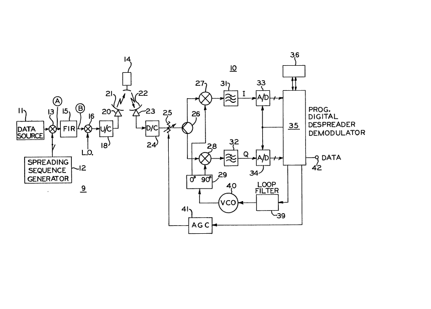
Referring now to Figure 1, there is shown a block diagram
illustrating an example of a satellite communication system
in accordance with the preferred embodiment of the present
invention. This system includes an earth station
transmitter 9 and an earth station receiver 10
communicating via a satellite 14. The transmitter 9
includes a source of data 11, which data is broadcast as a
spread spectrum signal modulated on an RF carrier signal.
The spreading of the data spectrum is accomplished through
what is generally shown as an exclusive OR circuit 13
receiving as a second input a spreading sequence signal
from sequence generator 12, having a chip rate f(c) which
is a multiple of the data bit rate. A unique sequence is
employed which is synchronized to the data bit stream and
repeated at the end of the sequence. By employing the
exclusive OR function, the bandwidth of the data signal is
increased to the bandwidth of the spread signal. The
resulting signal is modulated on a local oscillator
subcarrier by means of a modulator 16. In many satellite
communication systems, this modulation is accomplished
through BPSK modulation, i.e., binary phase shift keying
modulation. The modulated subcarrier signal containing the
- 20~5387
spread spectrum signal is frequency up converted to the
final transmit carrier frequency by an up converter 18. A
power amplifier 20 and antenna 21 are used to transmit the
modulated carrier signal bearing the spread spectrum signal
to an earth station receiver 10 via satellite 14.
Satellite 14 frequency shifts the modulated carrier signal
to a down link frequency signal. The down link signal is
broadcast to the receiver of earth station 10.
In carrying out the present embodiment of the invention,
spectrum shaping is employed by the use of an FIR filter
15. The FIR filter has a lowpass filter structure for
tailoring the spectrum of the spread spectrum signal. The
bandwidth of the filter corresponds to substantially one
half of the chip rate f(c). The amplitude response of the
filter is shaped to be maximally flat, with less than 1 dB
of ripple. This permits the power level to be maximized to
the 6 dBW/4 kHz limitation, per the FCC imposed limit.
The filtering provided by the FIR 15 can be explained in
terms of the spread spectrum plots shown in Figure 2, and
the filtered response shown in Figure 3. Referring to
Figures 2 and 3, it is clear that the spread spectrum
signal is of the form of SIN X, where X is frequency. It
should be recognized that each of Figures 2 and 3 represent
half of the transmit spectrum, once the carrier signal is
modulated, the other half being a mirror image to the left
of the Figures.
The required bandwidth of interest is the chip rate f(c),
or spreading frequency, which for the present example, is
1024 kilochips/second. Thus, since each of the foregoing
illustrations represent half of the bandwidth of interest,
the 512 KHz mark represents the practical 3 dB point for
the bandwidth of interest. As can be seen from Figure 3,
205S387
the amplitude function has minimum ripple in this area, as
contrasted to the SIN X function before filtering as shown
in Figure 2. The spectrum shown in Figure 3 may be
amplified such that any frequency components within the
bandwidth of interest are at the maximum power density
permitted by FCC regulations.
In order to achieve the spectrum shaping of Figure 3, the
FIR filter is selected to be a 6-pole Butterworth filter,
having an impulse response time inverse to a corresonding
receive filter impulse response.
To approximate the time inverse 6-pole Butterworth filter,
an FIR filter such as the one shown in block diagram form
in Figure 5 may be implemented. As illustrated, the FIR
filter 15 includes a plurality of delay elements 43 through
47, which produce a corresponding number of delayed signals
which are summed together after weighting by coefficients
CO_CN in mixers 50 through 53. The weighting coefficients
CO_CN for obt~;ning the filter functions of Figures 3 and 4
may be selected from well-known filter design references.
The weighted outputs from each of the mixers 50-53 are
combined in a final summation network 55.
It will be recognized that the weighting coefficients CO_CN
inverse 6-pole Butterworth filter may be implemented in
ROM. The resulting digital signal from the ROM may then be
converted from a digital signal to an analog signal prior
to applying the signal to BPSK modulator 16.
Having thus described a transmitter having a power spectrum
shaped to provide the maximum power over the bandwidth of
interest while maintaining the required power density
limit, a receive station 10 for the spectrum-shaped signal
may be described.
- 2055387
The earth station 10 receiver of Figure 1 includes a small
aperture directional antenna 22 for receiving the spread
spectrum signal transmitted on the satellite downlink
carrier. After passage through a first low noise
amplification stage 23, the carrier signal is applied to a
down converter 24. The down converter 24 converts the
spread spectrum downlink carrier signal to an intermediate
frequency signal bearing the spread spectrum modulated
data.
An attenuator 25 is shown as part of an AGC loop controlled
by an AGC amplifier 41. The resulting intermediate
frequency signal is split by power splitter 26 and applied
to a pair of mixers 27 and 28. The mixers 27 and 28 are
supplied with conventional orthogonal reference signals so
as to provide conventional I and Q b~h~n~ signals. The
I and Q baseband signals are filtered in a pair of low pass
filters 31 and 32.
These filters may be analog filters which are inexpensive
and which exhibit a 6-pole Butterworth response having 3 db
points at approximately the same bandwidth as the FIR
filter 15 in the transmitter of the earth station 9.
The filters 31, 32 are constructed to have a group delay
response as shown in Figure 7. The group delay of the FIR
filter 15, as shown in Figure 4, is the inverse of the
group delay for the analog receive filters. The filters on
the transmit and receive side are matched filters having a
combined response of S(T).H(T) selected to be approximately
~yquist, where S(T) is the FIR 15 filter transfer function
and X(T) is the transfer function of filters 31, 32. In
this manner, the matched filters 15 and 31, 32 provide for
a ~ m signal transfer.
2D55387
The filtered I and Q signals are then digitized in analog
to digital converters 33 and 34. A programmable digital
despreader 35 is provided which, under control of a
microprocessor 36, is configured to provide despreading and
demodulation of the signal, providing the demodulated data
signal on output terminal 42.
More particularly, the programmable digital despreader 35
receives microcode from the microprocessor 36. The
microcode configures the despreader 35 as depicted in
Figure 8 to provide spread spectrum demodulation. In this
configuration, the microprocessor 36 will provide the loop
filter 39 with drive signals for controlling the VCO 40 of
the baseband demodulator as well as an AGC signal for
ensuring a constant amplitude signal to the analog to
digital converters 33, 34.
In accordance with yet another feature of the invention,
the programmable despreader demodulator 35 is configured as
a programmable logic array to either provide the
despreading demodulator configuration shown in Figure 8, or
to provide a demodulator configuration which will
demodulate signals which have not been spread, as shown in
Figure 9. The programmability of the programmable logic
array 35, via the microprocessor 36 thus provides an earth
station capable of being rapidly configured under control
of microprocessor 36 for either demodulator mode.
Figure 8 is a block diagram depicting the programmable
logic array 35 as it is configured by the microcode
downloaded from the microprocessor 36 to provide the
standard despreader demodulation circuitry shown. This
includes a plurality of multipliers 48 through 53, fed by
three sequence signals PL, PE and PS. As is known in the
spread spectrum technology, three sequence signals
20~3~7
representing a synchronous sequence PS, an early sequence
PE and a late sequence PL, are generated from sequence
generator 77. These signals represent the spreading
sequence used at the transmitter for spreading the data
signal over the spectrum at the 1024 kilochip/second chip
rate f(c) signal. The results of multiplying the sequence
signals PL, PE and PS with the I and Q signals are
accumulated in adders/accumulators 56-61. Squaring
circuits 63-66 square the output signals of these adders/
acccumulators. The squared outputs are then summed in
summing circuits 68-70 to derive the error signal for
despreading the I and Q signals.
The synchronous (on time) sequence PS is multiplied by the
I and Q signals in multipliers 52, 53. The results are
accumulated in adder-accumulators 60, 61 and utilized as
control signals for the AGC and carrier recovery circuits.
The carrier recovery loop filter 74 is driven by a signal
from each of the adders-accumulators 60 and 61, thereby
controlling the frequency of the baseband demodulator VC0
40-
The signal for controlling the chip clock and symbol clocksand the remaining timing signals for the despreading
demodulator is derived from the squaring function circuits
63 through 66 and summation circuits 68, 69 and 70. A
symbol timing loop filter 75 filters the resulting signal
for controlling the phase and frequency of the VCX0 76.
By implementing the foregoing demodulator in a programmable
logic array, as has been mentioned, it is possible to
change the configuration of the demodulator from a
despreading to a non-spreading spectrum demodulator
configuration equivalent to a conventional BPSK
demodulator. Referring specifically to Figure 9, there is
205~387
shown a BPSK demodulator configuration obtained by
downloading the requisite firmware from the microprocessor
to the PLA 35. As depicted in Figure 9, the PLA is
configured to produce as output data on terminal 42 the I
channel data representing a digitized baseband signal free
from any carrier or intermediate frequency components.
Additionally, the symbol timing loop 75 is maintained as
well as the VCXO 76 for providing a symbol clock and other
timing signals needed to further process the data on
terminal 42. An AGC loop filter 73 and carrier recovery
loop filter 74, as is conventional in these systems,
operates from the I and Q signals to develop the respective
control signals for the AGC amplifier 41 and voltage
controlled oscillator 40.
Thus, as has been shown, the use of the programmable logic
array, under control of the microprocessor, provides for
the versatility of configuring different demodulator types
with only minimal operator intervention, and no change in
circuit hardware. Those skilled in the art will recognize
yet other embodiments encompassed by the claims which
follow.