Note: Descriptions are shown in the official language in which they were submitted.
CFO 8039 ~C~
2û~54û0
1 Method of Forming Crystal
BACKGROUND OF THE INVENTION
Field of the Invention
The present invention relates to a method of
forming a crystal, and particularly to a method of
forming a crystal by selectively growing monocrystal
on a substrate having a surface with a low nucleation
density.
The method of forming a crystal of the present
invention is preferably used for electronic devices
such as semiconductor integrated circuits, optical
integrated circuits and the like, optical devices,
magnetic devices, piezoelectric devices, surface
acoustic devices and the like.
Related Background Art
Monocrystal films used for semiconductor
devices and optical devices are generally formed by
epitaxially growing monocrystal on a monocrystalline
substrate.
For example, it is known that Si, Ge or GaAs
is epitaxially grown on a Si monocrystalline substrate
(silicon wafer) from a liquid phase, a vapor phase or a
solid phase thereof. It is also known that a GaAs or
GaAlAs monocrystal is epitaxially grown on a GaAs
monocrystalline substrate.
The semiconductor films formed by the above
205S~00
1 methods are used for producing semiconductor devices,
integrated circuits, light emitting devices such as
semiconductor lasers, LED and the like.
On the other hand, very high speed transistors
which use two-dimensional gases and superlattice
elements which use quantum wells have recently
actively been researched and developed. These devices
can be realized by high precision epitaxial techniques
such as MBE (molecular beam epitaxy) using super high
vacuum, MOCVD (metal organic chemical vapor deposition)
and the like.
Such epitaxial growth on a monocrystalline
substrate requires conformity in lattice constant and
thermal expansion coefficient between the
monocrystalline material of the substrate and the
epitaxially grown layer.
For example, although an Si monocrystalline
film can be epitaxially grown on sapphire used as an
insulator monocrystalline substrate, the crystal
lattice defects caused by the differenced between the
lattice constants at the interface and the diffusion
of the aluminum component of sapphire into the
epitaxial layer are problems in application to
electroniC devices and circuits.
As described above, it is known that the
conventional methods of forming a monocrystalline film
by epitaxial growth are significantly dependent on the
2055~
1 substrate material used. Mathews et al. investigated
combinations of substrate materials and epitaxially
grown layers (EPITAXIAL GROWTH, Academic Press, New
York, 1975, edited by J.W. Mathews).
Presently, the size of a substrate is about 6
inches in the case of an Si wafer and the size of a
GaAs or sapphire substrate is slightly increased.
In addition, since a monocrystalline substrate
is produced at high cost, the cost per chip is
increased.
The conventional methods of forming a
monocrystalline layer which enables the formation of
excellent devices have the problem that the kinds of
materials for the substrate are limited to a very
narrow range.
on the other hand, there have recently been
active research and development of three-dimensional
integrated circuits in which a semiconductor device is
laminated on a substrate in the direction of a normal
line thereof so that an increase in integration and
diversification of the function can be achieved.
In addition, large area semiconductor devices
such as solar cells, liquid crystal pixel switching
transistors and the like in which elements are arrayed
on inexpensive glass are increasingly actively
researched and developed year after year.
The both types of devices commonly require
-- 2055400
-- 4
1 the technique of forming a semiconductor film on an
amorphous insulator and then forming electronic
devices such as transistors or the like thereon.
Particularly, there is demand for the technique of
forming high-quality monocrystalline semiconductors
on an amorphous insulator.
In general, when a thin film is deposited
on an amorphous insulator substrate composed of Sio2,
the crystal structure of the deposited film is
amorphous or polycrystalline due to the absence of
long-distance order in the substrate material. The
terms "an amorphous film" represent a film assuming
the state order is held within a short range such as a
distance between adjacent atoms but is not held at a
longer distance, and the terms "a polycrystalline
film" represent a film comprising monocrystalline
grains having no particular crystal orientation and
gathering with grain boundaries which separate the
grains from each other.
For example, Si is deposited on SiO2 by a CVD
process, amorphous silicon is formed at a deposition
temperature of about 600 ~C or less, and
polycrystalline silicon comprising grains having a
size of several hundreds to several thousands A at a
deposition temperature of 600 ~C or more. However,
the grain size of the polycrystalline silicon formed
is significantly dependent on the formation
205S400
1 conditions.
Further, an amorphous or polycrystalline film
is molten and solidified by using an energy beam
generated from a laser or a rod heater to form a
polycrystalline film comprising grains having a large
size of several microns or millimeters (Single Crystal
Silicon on Non-Single Crystal Insulators, Journal of
Crystal Growth Vol. 63, No. 3, 1983 edited by G.W.
Cullen).
As a result of measurement of electron
mobilities of transistors formed on the thin films
formed by the above method and having various crystal
structures, the mobility of amorphous silicon was
~ 0.1 cm tV~sec, the mobility of polycrystalline
silicon comprising grains having a size of several
hundreds A was 1 to 10 cm2/V sec, and the mobility of
polycrystalline silicon formed by melting and
solidification and comprising large grains was
substantially the same as that of monocrystalline
silicon.
These results show that the electrical
properties of the device formed in a monocrystalline
region within a crystal grain are significantly
different from those the device formed on a region
including a grain boundary.
Namely, the film deposited on an amorphous
substrate has an amorphous or polycrystalline
2055400
l structure, and the device formed on the deposited film
has poor properties, as compared with the device
formed on a monocrystalline layer. The application
of such a device formed on a deposited film is limited
S to a simple switching element, a solar cell, a
photoelectric conversion element or the like.
Methods of depositing a crystal layer on an
amorphous substrate are roughly divided into the
following two methods.
One method is a method in which an amorphous
insulator (for example, SiO2) is coated on a
monocrystal (for example, Si) used as a substrate and
then partially removed to expose the surface of the
ground monocrystal, and a monocrystalline region is
then formed on the amorphous insulator layer by
horizontal epitaxial growth from a vapor phase, solid
phase or liquid phase using the exposed ground
monocrystal surface as a seed crystal.
The other method is a method of growing a
crystal thin film directly on a substrate without
using a monocrystal as a substrate.
As described above, since the surface of an
amorphous substrate has no long-distance order, as
the surface of a monocrystalline substrate, but
holds short-range order only, the deposited thin film
at best has a polycrystal structure in which grain
boundaries are randomly present. In addition, since
- - - 20 5540~
I both the long-distance order and anisotropv defining
crystal orlentation (orientation in the normal
direction of the substrate and in the surface) are
absent in the surface of an amorphous substrate, the
crystal orientation of a layer formed on the substrate
cannot be controlled.
Name]y, a problem of deposition of a
monocrystal on an amorphous substrate is to establish
a technique of controlling boundary positions and
crystal orientation.
A description will now be given of
conventional methods of controlling boundary positions
and crystal orientation and the problems thereof.
In regard to the control of boundary positions,
EP244081Al, published November 4, 1987 discloses that
boundary positions can be determined by artificially
previously defining nucleation positions.
In this technique, for example, Si3N4 is
localized on SiO2, Si monocrystal are grown from Si3N4
serving as nucleation sites, and grain boundaries are
formed by collision between the crystals grown from
adjacent nucleation sites, thereby determining
boundary positions.
Another technique is also proposed in which
a non-monocrystalline material serving as primary seed
is previously patterned in stead of nuclei which are
spontaneously produced at nucleation positions, the
?
r ~.
- 8 - ~ ~ 5 5 4 ~ O
1 material is changed to monocrystal serving as seed
crystals by employing aggregation (Japanese Patent
laid-Open No. 1-132117 published May 24, 1989 - Canon K.K.)
The plane orientation (crystal orientation
in the direction vertical to the substrate) of the
crystals grown by the above techniques is determined
by the factors such as stabilization of interfacial
energy at the amorphous interface with the substrate,
stabilization of free surface energy, relaxation of
internal stress and so on during the generation of
nuclei or aggregation of primary seeds. However,
it is difficult to obtain complete orientation in a
single direction, and main plane orientation and
other orientations are frequently mixed. Particularly,
one in-plane crystal orientation is not determined
because the nucleation surfaces or aggregation
surfaces are amorphous and do not have anisotropy.
On the other hand, H. I. Smith first showed
that anisotropy caused by irregularity is artificially
provided on the surface of an amorphous substrate by
lithography so that the crystal orientation of KC1
deposited on the substrate can be controlled, and
named this technique "graphoepitaxy" (H. I. Simth and
D. C. Flanders, Applied Physics Letters Vol. 332,
pp349, 1978) (H. I. Smith, U.S. Patent No. 4,333,792,
1982).
It was later confirmed that an artificial
ti
20~Q0
g
1 relief pattern formed on the surface of a substrate
affects the crystal orientation in the growth of grains
in a Ge thin film (T. Yonehara, H. I. Smith, C. V. Thompson
and J. E. Palmer, Applied Physics Letters, Vol. 45, pp.
631, 1984) and in the initial growth of Sn (L. S. Darken
and D. H. Lowndere, Applied Physics Letters Vol. 40, pp.
954, 1987).
Although it was found that graphoepitaxy has an
effect on the orientation of each of separate KCl or Sn
crystals deposited in an initial stage, there have also
been reports of continuous layers, e.g., an Si layer
formed by laser annealing crystal growth after deposition
(M. W. Ceis, D. A. Flanders and H. I. Smith, Applied
Physics Letters, Vol. 35, pp. 71, 1979) and a Ge layer
formed by solid phase growth (T. Yonehara, H. I. Smith,
C. V. Thompson and J. E. Palmer, Applied Physics Letters,
Vol. 45, pp. 631, 1984).
However, in the cases of Si, Ge layers, although
orientation is controlled to some extent, a crystal group
is arranged in a mosaic pattern, and grain boundaries are
randomly present between crystals having slightly different
crystal orientations. It is thus impossible to obtain
monocrystal uniformly arranged in a large area.
The reason for this is that the three-dimensional
crystal orientations of respective crystals are not
completely the same, and the nucleation positions cannot
be controlled by a surface relief pattern.
2055400
- 10 -
1 SUMMARY OF THE INVENTION
It is an object of the present invention
to provide a method of forming a crystal which is
capable of growing monocrystal having grain boundaries
at controlled positions and the same plane orientation
and in-plane orientation.
It is another object of the present invention
to provide a method which is capable of uniformly
and simply forming monocrystal having a single
orientation in a large area without producing a
plurality of orientations other than main
orientation.
BRIEF DESCRIPTION OF THE DRAWINGS
Fig. lA is a schematic drawing showing an
example of a primary seed used in a method of forming
a crystal of the present invention;
Figs. lB to lD are schematic drawings
respectively showing the shapes of insulators
surrounding primary seed;
Figs. 2A to 2D are schematic drawings showing
an example of methods of forming crystals of the
present invention;
Figs. 3A to 3C are schematic drawings showing
an example of processes of forming a primary seed in
a method of forming a crystal of the present
20~00
11
l invention;
Figs. 4A to 4D are schematic drawings showing
another example of processes of forming a primary
seed in a method of forming a crystal of the present
lnventlon;
Figs. 5A to 5C are schematic drawings showing
an example of processes in a method of forming a
crystal of the present invention;
Fig. 6A is a schematic drawing showing an
example of a primary seed in a method of forming a
crystal of the present invention;
Figs. 6B to 6D are schematic drawings
respectively showing the shapes of insulators
surrounding a primary seed;
Figs. 7A to 7D are schematic drawings showing
an example of processes in a method of forming a
crystal of the present invention;
Figs. 8A to 8C, Figs. 9A to 9D and Figs. lOA
to lOC are schematic drawings respectively showing
examples of processes in a method of forming a crystal
of the present invention;
Fig. 11 is a schematic drawing showing an
example in which a primary seed is formed in a
recessed portion formed in a substrate;
Fig. 12 is a partially sectional view of the
recessed portion and the primary seed shown in Fig.
11; and
2055~0~
- 12 -
l Figs. 13A to 13F are schematic drawings showing
another example of processes in a method of forming a
crystal of the present invention.
DETAILED DESCRIPTION OF THE PREFERRED EMBODIMENTS
Preferred embodiments of a crystal forming
method of the present invention are described below.
A method of forming a crystal of the present
invention comprises disposing primary seed having
side walls and a bottom, all of which contact with
an insulator, having a rectangular prismatic or cubic
shape and a volume sufficiently small to singly
aggregate on a substrate having a surface with a low
nucleation density or in recessed portions formed in
the substrate; performing heat treatment for inducing
aggregation in the primary seed to form
monocrystalline seed crystal having controlled plane
orientation and in-plane orientation; and performing
crystal growth treatment for selectively growing
monocrystal using the seed crystal as starting point.
In another preferred form, the method of
a forming crystal of the present invention comprises
disposing monocrystalline seed crystal on a substrate,
and growing monocrystal using the seed crystal as
starting point, wherein recessed portion having at
least an angular portion formed by three surfaces
including the bottom and two sides, all of which
2D~5~Q~
- 13 -
l vertically contact with each other, is formed in the
surface of the substrate so that primary seed is
disposed in the angular portion so as to contact with
the three surfaces and is then singly aggregated by
heat treatment to form monocrystalline seed crystal,
and monocrystal is grown using the seed crystal as
starting point.
In a further preferred form, the method of
forming a crystal of the present invention comprises
disposing a primary seed having surfaces, all of which
contact with an insulator, and a rectangular prismatic
or cubic shape on a substrate having a surface with a
low nucleation density or in a recessed portion formed
in the substrate; melting and then solidifying the
primary seed to form monocrystal having controlled
plane orientation and in-plane orientation; at least
partially removing the insulator covering the
monocrystal to expose the monocrystalline
surface; and selectively growing monocrystal using the
exposed monocrystal as starting point by crystal
growth treatment.
In a still further preferred form, the method
of forming crystal of the present invention comprises
disposing a seed crystal on a substrate and growing
monocrystal using the s~ed crystal as starting point,
wherein recessed portion having at least an angular
portion formed by three surfaces including the bottom
20S5~00
- 14 -
l and two sides, which vertically contact with each
other, is formed in the surface of the substrate,
primary seed is disposed in the angular portions so
as to contact with the three surfaces and molten and
then solidified to form monocrystalline seed crystal,
and monocrystal is grown using the seed crystal as
starting point.
The method of forming crystals of the present
invention enables the selective growth of monocrystal
from monocrystalline seed crystal serving as starting
point and having controlled plane orientation and
in-plane orientation and thus enables the formation of
monocrystal having controlled grain boundaries and
uniform plane orientation and in-plane orientation
on an insulating substrate.
The present invention also permits a primary
seed of which has a rectangular prismatic or cubic
shape having surfaces in contact with an insulator
and which is changed to monocrystal by melting and
solidification to be changed from non-monocrystal
to monocrystal having uniform plane orientation and
in-plane orientation. When a semiconductor material
is selectively grown by using the monocrystal as seed
crystal, SOI devices can be formed with controlled
boundary positions and uniform plane orientation and
in-plane orientation.
The present invention is capable of completely
2055~;01~
- 15 -
l controlling the boundary positions (number) and
orientation, which cause deviations in properties of
SOI device, and thus forming device with high
uniformity.
In addition, since melting and solidification
on the three vertical surfaces at an angular portion
of recessed portion in the substrate has good effects
on the plane orientation and in-plane orientation of
seed crystals, the present invention is capable of
uniformly and simply forming monocrystal over a large
area with a single orientation without a plurality
of orientations other than main orientation.
Further, since the three vertical surfaces
at an angular portions of recessed portion in the
substrate have good functions as equivalent surfaces
to the stable orientation structure of the seed
crystal formed by aggregation, the present invention
is capable of uniformly and simply forming monocrystal
over a large area with a single orientation without
a plurality of orientations other than main
orientation.
The plane orientation of a crystal formed by
aggregation or melting and solidification is
determined so that the free surface energy of the
crystal and the interfacial energy at the interface
with the substrate are minimum, as described above.
For example, when polycrystalline Si is aggregated
~055~00
- 16 -
1 on SiO2, since the free surface energy of Si is
minimum on the (111) plane, the plane orientation is
produced along the (111) plane. On the other hand,
since the Si-SiO2 interfacial energy is stable on
the (100) plane, the interfacial energy is conformed
to the (100) plane. In addition, since
polycrystalline Si generally has (110) orientation
depending upon the deposition temperature, the factor
of the initial state also has an influence on the
orientation. As a result, Si aggregated on SiO2 is
relatively strongly oriented on the (111) plane, with
having (110) orientation with a ratio of about 1/2 to
1/3 of (111) orientation in terms of the reflection
intensity in X-ray diffraction. In X-ray diffraction,
weak peaks of (100), (311), (331), (422) and so on
are also observed. Possible reasons for domination of
(111) orientation are that aggregated Si comprises
semispherical crystal and has a surface area
significantly greater than the area of the interface,
and that the stabilization of free surface energy
among the factors for determining orientation is
the most important factor.
However, since the above-described many
factors have influence on orientation, it is very
difficult to completely control a single orientation
even by changing the material of the substrate surface
or aggregation conditions. Much more, it is
20S5400
- 17 -
l substantially impossible to control the in-plane
orientation by aggregation on a two-dimensional
surface.
The inventors thus conceived an arrangement
in which the stabilization of interfacial energy is
a main factor which determines orientation for
controlling a single orientation and then an
arrangement in which in-plane orientation is further
controlled. Both arrangements can be satisfied by the
arrangement of the present invention which is obtained
by aggregating a primary seed having a rectangular
prismatic or cubic shape formed so as to be surrounded
by an insulator in contact with the sides and the
bottom thereof and having a small volume sufficient to
singly aggregate.
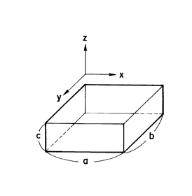
A typical example of primary seed is shown
in Fig. lA. However, the rectangular prism (or cube)
shown in the drawing is surrounded by an insulator
in contact with all the surfaces thereof excepting
one surface (the upper surface of the xy plane).
Although the stabilization of interfacial
energy during aggregation is affected by the bottom
of an primary seed and only one of the surfaces of
an insulator in conventional methods, in the crystal
2S forming method of the present invention, the five
surfaces contribute to the stabilization of the
interfacial energy and respectively intersect the
2055400
- 18 -
l adjacent surfaces. The method of the present
invention thus has the advantage that the five
surfaces have the functions as equivalent surfaces
to the stable orientation structure of a crystal
formed by aggregation. In addition, since the exposed
area is smaller than that in the conventional methods,
the method of present invention has the effect of
decreasing the influence of stabilization of
interfacial energy on changes in the structure during
aggregation. As a result, the control of orientation
(including in-plane orientation) which is produced in
graphoepitaxy or growth of Ge grain which takes plane
in a surface relief structure can be reproduced in
an aggregation system comprising primary seeds.
Embodiments of the present invention are
described below with reference to Figs. lA to lD and
Figs. 2A to 2D.
Embodiment
A description is first made of the shape
and size of a primary seed which is the most important
in the present invention.
Although the shape of primary seed must be
a rectangular prismatic or cubic shape, as described
above, strictly speaking, the objects of the present
invention can be achieved even if the shape of the
primary seed is not a completely rectangular prismatic
or cubic shape. Conversely, if primary seed has a
- 205S~00
- 19 -
1 completely rectangular prismatic shape, it is difficult
to provide a monGcrystalline seed with specified
orientation in the direction vertical to a surface of an
insulator without deviation of several second degrees
even by aggregating the primary seed surrounded by the
insulator. If the crystals grown from such seed crystals
collide with each other, grain boundaries are invariably
produced. In the present invention, it is therefore
sufficient that the position of grain boundaries is
controlled, and no deviation occurs in the properties of
devices due to deviations in orientation during the
production of devices. Namely, deviations from design
values which are caused by sagging or over etching
produced at the pattern edge in a photolithographic process
or etching process, i.e., an angle of several degrees or
less, is allowable.
The terms "a rectangular prismatic or cubic
primary seed surrounded by an insulator in contact
with the side walls and the bottom thereof" represent,
for example, the shape shown in Figs. lB, lC or lD.
Figs. lB and lC show so-called "buried type"
shapes. These buried type shapes are formed by
partially patterning the surface of an insulator
substrate 102 with squares or rectangles and etching
the surface to form rectangular prismatic or cubic
space and respectively burying the primary seed in
the space formed. In this case, a primary seed 101
2055~10~
- 20 -
l to be buried may have a shape which causes the exposed
surface to be at the same level as that of the surface
of the insulator, i.e., which makes the whole surface
flat, as shown in Fig. lB, or a shape which causes
the exposed surface to be at a level lower than that
of the insulator surface, i.e., which has a height
(the c value shown in Fig. lA) smaller than the
etching depth. On the other hand, Fig. lD shows "a
side-wall formation type". This type is formed by
patterning a primary seed in a rectangular prismatic
or cubic region on an insulator substrate or a
substrate having an insulator surface layer and then
forming an insulator on the side walls of the primary
seed with leaving the upper surface so as to surround
lS the primary seed.
In any one of the cases, the material of the
side walls need not to be the same as the material
of the substrate 102. For example, in the case of the
buried type, a rectangular prismatic or cubic space
is formed in the substrate, and an insulating film is
formed in the space formed so that the surfaces of
the insulating film are used as insulator side walls.
The size of the primary speed is described
below. In the shape shown in Fig. lA, the primary
seed has a, b values which are preferably a, b < 2 ~m
(both values may be the same, a = b), more preferably
1 ~m or less, and most preferably about 0.5 ~m.
20S5~00
. ,
- 21 -
1 This is because, if the a, b values exceed 2 ~m, the
primary seed is not singly aggregated but aggregated
in a form divided into a plurality of portions.
Whether the seed crystal is divided or not
significantly depends upon the thickness of the film,
i.e., the c value, and if the aspect ratio between the
value a or b and the value c is high, the seed crystal
is easily divided. The reason for determining the
optimum a, b values of about 0.5 ~m is that if the a,
b values are set to be 0.5 ~m or less, a general
semiconductor photoprocess cannot be easily applied
to the primary seed. On the other hand, the thickness
(= c) of the primary seed is preferably 0.05 to 0.5
~m, and more preferably 0.1 to 0.4 ~m. The optimum
thickness is determined by the values a and b.
Although the smaller the thickness is, the more easily
aggregation takes place, if the thickness is less than
0.05 ~m, the values a, b must be decreased for singly
aggregating the primary seed. This causes the
problems that a general photoprocess cannot be easily
applied, as described above, and that the effect of
the side walls for controlling orientation is
decreased. If the value c is greater than 0.5 ~ m,
aggregation does not easily take place. The optimum
value of the thickness is therefore within the range
of 0.5 ~ c ~ 0.05 (~m).
Examples of materials that can be used for
- 2û55~00
- 22 -
l the primary seed to be aggregated include
semiconductor elements such as Si, Ge, Sn and the
like; metals such as Au, Ag, Cu, Pt, Pd and the like;
alloys; compounds and mixtures thereof.
An amorphous insulator such as SiO2, SiXNy,
SiON or the like is used as an insulator which forms
non-nucleation surfaces. The composition of the
insulator which forms the non-nucleation surfaces
need not to be the same as that of the insulator in
the portions contacting with the primary seed.
The process in an embodiment of the present
invention is described below with reference to Figs.
2A to 2D.
As shown in Fig. 2A, a substance used for
primary seeds 201a, 201b is buried in small recessed
portions 203a, 203b in an insulator substrate 202 or
a substrate having a surface layer covered with an
insulator. Each of the recessed portions 203a, 230b
has a rectangular prismatic or cubic form. As
described above, the recessed portions 203a, 203b
need not to be formed in the substrate, and the side
walls of each of the primary sees 20la, 20lb may be
surrounded by an insulator in contact therewith.
Although Si, Ge or the like is used as a
material for the primary seeds 201a, 201b, as
described above, a polycrystal or an amorphous
material may be used.
- 2055~00
lAs shown in Fig. 2B, the primary seeds 20la,
201b are then subjected to heat treatment in an
atmosphere of hydrogen so that aggregation takes
place to form seed crystals 204a, 204b having uniform
plane orientation and in-plane orientation. Although
the conditions of heat treatment depend upon the
material use for the primary seeds and the volume
thereof, when the material for the primary seeds is
a semiconductor element such as Si, Ge or the like,
10the temperature is generally about 700 to 1100 ~C.
Although the pressure may be atmospheric pressure,
heat treatment is preferably performed under reduced
pressure (several Torr to 200 Torr) so that
aggregation easily takes place. Doping of the
primary seeds with large quantities of impurities
(phosphorus, boron, arsenic or the like) has the
effect of decreasing the aggregation starting
temperature.
As shown in Fig. 2C, monocrystals are
selectively grown from the monocrystalline seed
crystals formed by aggregation and serving as centers.
The crystal growth is effected by the CVD process.
For example, when Si crystals are grown, the growth
can be achieved at a temperature of 800 to 1200 ~C
by using as a source gas a silane type gas such as
SiH4, Si2H6 or the like, a chlorosilane type gas such
as SiH2Cl, SiHCl3, SiCl4 or the like, or a
20~5 413~
- 24 -
1 fluorosilane gas such as SiH2F2, SiF4 or the like,
which source gas is mixed with etching gas such as
HCl or the like in H2 dilution gas.
A grain boundary 206 is produced between
the crystal 205a grown from the seed crystal 204a
and the crystal 205b similarly grown from the adjacent
seed crystal 204b at an intermediate position between
the adjacent seed crystals which are first patterned.
If the two crystals 205a, 205b originally have the
completely same orientation ir.cluding in-plane
orientation, a continuous crystal film is formed
without any grain boundaries. However, in fact,
there are slight deviations in crystal orientation
between crystals, grain boundaries are formed in most
cases.
Each of the grown crystals 205a, 205b is a
monocrystal and thus has a crystal face (facet)
peculiar to the crystal. When electronic devices
are formed on the grown crystals, therefore, the
crystals are polished to form a flat surface as
occasion demands, as shown in Fig. 2D.
Another embodiment of the present invention
is described below.
The crystal forming method comprises disposing
monocrystalline seed crystal on a substrate, and
growing monocrystal using the seed crystal as starting
point, wherein recessed portion having at least an
2055400
- 25 -
l angular portion where three surfaces comprising the
bottom and two sides vertically contact with each
other is formed in the substrate, a primary seed is
disposed in the angular portions so as to contact with
the three surfaces and then subjected to heat
treatment for singly aggregating the primary seed
to form monocrystalline seed crystal, and monocrystal
is then grown using the seed crystal as starting
point.
Fig. 11 is a schematic drawing showing a
recessed portion (crystal growth region) formed in
a substrate, and a primary seed formed in the recessed
portion. Fig. 12 is a sectional view of the recessed
portion and the primary seed shown in Fig. 11.
In the example shown in Figs. 11 and 12, an
primary seed 1112 is formed so as to contact with the
sides 1113, 1114 and the bottom 1115 of a recessed
portion (crystal growth region) 1111. In this
example, the sides 1113, 1114 and the bottom 1115 must
be respectively positioned as vertical surfaces. The
three surfaces 1113 to 1115 have go~d functions during
aggregation, as described above.
The terms "the three surfaces 1113 to 1115
are vertical to each other" represent that the
surfaces are strictly vertical or substantially
vertical to each other. For example, even if error
of several degrees or less is produced in the angle
20554Q0
- 26 -
l of the surfaces due to sags produced at pattern edges
or deviations from the design values, which are
caused by over etching, in a usual photolithographic
process, etching process or the like, the surfaces
are considered vertical in the present invention.
In this case, the effects of the present invention can
be obtained.
Even if the surfaces 1113 to 1115 are formed
in substantially completely vertical surfaces, it is
impossible that many monocrystalline seed crystals
have specified orientation without deviation of
several seconds degrees. In the present invention,
therefore, the three surfaces may be vertical to the
extent which causes no deviation in the properties
of devices to be produced due to deviation in
orientation during the production of devices in many
crystal regions.
The shape of the primary seed 1112 is not
particularly limited. However, since the primary
seed 1112 is disposed so as to contact with the three
surfaces 1113 to 1115, as shown in Fig. 11, the
contact portions of the primary seed 1112 are
inevitably three vertical surfaces. The shapes of
the portions of the primary seed 1112, which do not
contact with the surfaces 1113 to 1115, are not
particularly limited, and the portions may be formed
in any shapes which can be easily formed.
2055~00
- 27 -
1 The size of the primary seed 1112 may be
sufficient small to singly aggregate. When the
primary seed 1112 has a rectangular prismatic shape,
as shown in Fig. 11, the length of each of the two
sides a and b of the bottom is preferably 2 ~m or
less, more preferably 1 ~m or less, and most
preferably about 0.5 ~m. If the length exceeds 2 ~m,
the primary seed 1112 is sometimes aggregated in a
form divided into a plurality of portions, not in a
single body. Such a plurality of portions produced
do not serve as seed crystals for growing a
monocrystal. However, whether the primary seed 1112
is divided or not during aggregation significantly
depends upon the value of the thickness (height) c
of the primary seed. If the aspect ratio between
the value a or b to the value c is high, the primary
seed 1112 is easily divided during aggregation.
It is preferable that both the values a and
b are at least 0.1 ~m. If these values are less
than 0.1 ~m, there is the tendency that the control
of orientation caused by interfacial stabilization
energy becomes difficult due to a significant decrease
in the bottom area. In addition, when a usual
photolithographic apparatus is used, it is difficult
to pattern with a length of less than 0.1 ~m. The
values a and b need not to be the same.
The thickness (height) c of the primary seed
-- 2055400
- 28 -
l 1112 is preferably 0.05 ~m to 0.5 ~m, and more
preferably 0.1 ~m to 0.4 ~m. The optimum value of
the thickness c is determined by the values a and b.
In fact, the smaller the value c, i.e., the thinner
the primary seed 1112, the more easily aggregation
takes place. However, if the value c is 0.1 ~m or
less, since the values a and b must be also decreased
so that the primary seed is not divided during
aggregation, as ~escribed above, the effects of the
surfaces 1113 to 1115 on the control of in-plane
orientation are decreased. It is also difficult to
apply a general photoprocess. If the value c exceeds
0.5 ~m, there is the tendency that aggregation does
not easily take place.
Even when the shape of the primary seed 1112
is not a rectangular prism, it is preferable that
the sizes of the portions in direct contact with the
surfaces 1113 to 1115 are values equivalent to the
above values which may be regarded as standard values.
Examples of materials that can be used as
the material for the primary seed 1112 include
semiconductor elements such as Si, Ge, Sn and the
like; metals such as Au, Ag, Cu, Pt, Pd and the like;
alloys, compounds and mixtures thereof, all of which
are generally known as materials for primary seeds.
Various materials such as amorphous insulators
such as SiO2, SiXNy, SioN and the like, which are
2055400
- 29 -
l generally known as substrate materials for forming
crystals, can be used for a substrate 1110 having
the recessed portlon 1111. It is effective to use
a substrate having a relatively low nucleation density
over the whole substrate or only on a surface thereof.
It is more effective to use a substrate comprising
an amorphous insulator over the whole substrate or
only on a surface thereof.
The processes in the above-described
embodiment of the present invention are described with
reference to Fig. 13.
As shown in Fig. 13A, recessed portions 1301
serving as crystal growth regions are first formed
in a substrate 1300. Although the plane shape of
each of the recessed portions 1301 may be patterned
so that a portion where the primary seed is disposed
is formed in a desired angular portion, a square
or rectangle is preferable. Although the depth of
the recessed portion 1301 may be any desired value,
the value of the depth is preferably the same as
the working thickness of the film later grown.
Although the method of forming the recessed portions
1301 is not particularly limited, for example, RIE
(reactive ion etching) is more preferable that wet
etching using an etching solution because the sides
1303 of the recessed portion 1301 formed by the former
method are more vertical to the bottom than the sides
- 2U~5~00
- 30 -
1 formed by the later method.
As shown in Fig. 13B, a material 1302' for
the primary seeds is then deposited. As described
above, Si, Ge, Sn or the like can be used as the
material 1302', and the material 1302' may be either
polycrystalline or amorphous. Although the preferable
value of the thickness of the deposited film is
described above, the value of the thickness must be
smaller than the depth of the recessed portion 1301.
Examples of deposition methods include an evaporation
process, a sputtering process, a CVD process and
the like. However, the evaporation process and
sputtering process, both of which exhibit poor step
coverage, are preferable because it is undesirable
that the primary seed material 1302' unnecessarily
remains on the sides of the recessed portions 1301
during the latter process.
Etching is then performed with leaving the
primary seed 1302 in a desired angular portion in
the crystal growth region, as shown in Fig. 13C.
The etching may be performed by either a dry method
using RIE or a wet method using a solution. The
preferable values of the size of primary seed 1302
is as described above with reference to Fig. 11.
The primary seed 1302 is then subjected to
heat treatment for aggregation in an atmosphere of
hydrogen to form seed crystal 1206 having uniform
205S400
- 31 -
l plane orientation and in-plane orientation, as shown
in Fig. 13D. Although the conditions of the heat
treatment depend upon the material of the primary
seed 1302 and the volume thereof, when the primary
seed material is a semiconductor element such as Si,
Ge or the like, the temperature of the heat treatment
is generally about 700 to 1100 ~C. Although the
pressure may be atmospheric pressure, aggregation
is easily produced by the heat treatment at reduced
pressure (several Torr to 200 Torr). In addition,
doping of the primary seed 1302 with large quantities
of impurities (phosphorus, arsenic, boron or the
like) has the effect of decreasing the aggregation
starting temperature.
Crystal 1307 is then selectively grown from
the seed crystal 1306 serving as centers by the CVD
process or the like, as shown in Fig. 13E. For
example, when Si crystal is grown by the CVD process,
a silane type gas such as SiH4, Si2H6 or the like,
a chlorosilane type gas such as SiH2Cl2, SiHCl3, SiC14
or the like, or a fluorosilane type gas such as
SiH2F2, SiF4 or the like may be used as a source gas.
The Si crystal can be grown by mixing the source gas
with etching gas such as HCl, HF or the like in H2
dilution gas. The crystal growth by the CVD process
may be performed at a temperature within the range of
about 800 to 1200 ~C and pressure within the range
2Q 554~
~ - 32 -
1 of several Torr to about 200 Torr. The crystal
growth may be performed until the recessed portion
serving as the crystal growth region is completely
filled with crystal. The grown crystal 1307 has a
facet peculiar to a monocrystal. In this way, the
grown crystal 1307 can be easily deter~ined by the
size and shape of the recessed portion 1301.
As shown in Fig. 13F, the portion of the
crystal 1307 which protrudes from the recessed
portion 1301 is then removed so that the substrate
1300 and the crystal 1307 are flattened, whereby
devices or the like can be easily preferably formed
on the flat surface, and circuits can also easily
be formed.
The flattening is preferably performed by,
for example, a selective polishing method. The
selective polishing method includes the two types
of methods below. One of the methods is
"mechanochemical polishing" in which chemical
reaction with Si is produced by using an alkali
solution, and the reaction product is removed
(Hamaguchi, Endoh, Bulletin of the Applied Physical
Society, Vol. 56, No. 11, pp. 1480). The other
method is "mechanical polishing (Japanese Patent
published August 21, 1990 - Canon K.K.)
Laid-Open No. 2-209730 /which employs a difference
in mechanical polishing rates for polishing only a
substance to be polished (corresponding to the
-'
2055400
- 33 -
1 crystals 1307 shown in Fig. 13) having a high mechanical
polishing rate using abrasive grains of colloidal silica
or the like, and stopping polishing on the stopper
surface (corresponding to the substrate 1300 shown in
Fig. 13) having a low mechanical polishing rate. Although
the later mechanical polishing is effective for the case
of random crystal orientation, since the crystal grown in
the present invention has uniform orientation, either of
the above methods can be used. From the viewpoint of
this, the method of present invention is excellent.
Although the above crystal forming method of
the present invention employs aggregation, the crystal
forming method of the present invention which employs
melting is described below.
For example, when polycrystalline Si is
melted and solidified on SiO2, since the surface
energy of Si itself is stable in (111) orientation,
but Si-SiO2 interfacial energy is stable in (100)
orientation, the strong function of the stabilization
factor of the interfacial energy results in (100)
orientation. However, the Si film has (100)
orientation with respect to the plane of the
substrate, but the orientation in the plane of the
substrate is not at all controlled. In addition,
when a film formed by simply melting and
solidification, since there are many solidification
starting points in the plane, many grains are formed.
2055400
- 34 -
1 and random grain boundaries are consequently produced.
In the present invention, the inventor
conceived a structure for controlling the in-plane
orientation of each grain and the positions of the
grain boundaries produced by slight deviation in
orientation.
In the control of orientation, it was first
confirmed that the orientation vertical to the plane
of the substrate is controlled to predetermined
orientation by melting and solidifying the film
material. Since no information about in-plane
orientation is provided, information about the
control of horizontal orientation is provided by
forming the side walls (surfaces) vertical to the
plane of the substrate. The side walls are formed
so that four surfaces are vertical to each other,
i.e., the portion surrounded by the surfaces forms
a rectangular prism or a cube, thereby providing
information about orientation control from the four
directions. In addition, since the rectangular
prism or cube formed must comprise a monocrystal
containing no grain boundary during melting and
solidification, and since the walls must affect the
whole primary seed having a rectangular prismatic
or cubic shape, the rectangular prism or cube must
be designed so as to have an appropriate volume.
Typical vaues of the size of the rectangular prism
2055~0~
1 or cube are described below.
The position of grain boundary can be
controlled by patterning primary seed having a
rectangular prismatic or cubic shape at desired
positions. Namely, when primary seeds are patterned
at desired two positions, crystals are respectively
grown from the primary seeds and collide with each
other at just an intermediate position between the
two points to form a grain boundary. For example,
when primary seeds are patterned at lattice points
at distances Q, grain boundaries are formed at
intermediate positions between the respective lattice
points. As a result, square crystals each having
sides Q are regularly arranged in a lattice form.
Although it is thought that when crystals having
completely uniform plane orientation and in-plane
orientation collide with each other, no grain boundary
is generated, grain boundaries are in fact produced
because it is difficult to form and grow seed crystals
without deviation of only 1 second degree in the
direction vertical to the substrate and the in-plane
direction thereof. In short, it is sufficient that
the positions of grain boundaries are controlled, and
no deviation is produced in the properties of devices
due to deviation in orientation during the production
of the devices. Slags produced at the pattern edges
or deviations from the design values, which are caused
20~00
- 36 -
1 by over etching, in a usual photolithographic process
or etching process, i.e., angles of several degrees
or less, are allowable.
A description will now be made of the method
of forming a crystal film having controlled plane
orientation and in-plane orientation on an insulating
substrate using the seed crystals formed on the basis
of the above-described idea.
The shape and volume of a primary seed are
described below. As shown in Fig. 6A, a primary seed
has a rectangular prismatic shape (or a cubic shape
(a = b = c)). This is because when a certain
orientation is preferential in one surface of a
rectangular prism or cube, orientations equivalent
to that orientation are preferential in all the other
surfaces thereof.
The volume of a primary seed must be
sufficiently small to generate no grain boundary
in the primary seed during melting and solidification,
and the area of the sides are sufficinetly large to
stably determine in-plane orientation, as described
above. Specifically, the value a of the primary
seed shown in Fig. 6A is preferably within the range
of 0.1 ~m to 5 ~m, and more preferably within the
range of 0.5 ~m to 2 ~m, assuming that a = b. The
optimum value depends upon the materials for the
primary seed and the substrate. The minimum value
205S400
- 37 -
l is determined by the limit value of precision of
the photolithographic method or the minimum area
which permits the stabilization energy at the
interface with the substrate to control orientation.
The maximum value is experimentally determined so
that no grain boundary is produced during
solidification. However, this maximum value is
related to the value of the height c of the sides.
The value of the height c of the sides of
the rectangular prism or cube is preferably within
the range of 0.1 ~m to 2 ~m, and more preferably
within the range of 0.3 ~m to 1 ~m. The optimum
value depends upon the values a and b and the material
for the primary seed. The minimum value is determined
to be a minimum value which allows the sides to affect
the determination of in-plane orientation. The
maximum value is determined to be a value which does
not cause the formation of grain boundary during
solidification.
All the surfaces of a primary seed must be
covered with an insulator, as shown in Figs. 6B,
6C and 6D. Figs. 6B and 6C respectively show
"buried types" of primary seeds. In the buried
types, the surface of an insulator substrate 601
is partially patterned with squares or rectangles
and then etched to form rectangular prismatic or
cubic shapes in the substrate, a primary seed 602
205~400
- 38 -
1 is respectively buried in the spaces, and an
insulating film is then formed thereon. In this
case, the upper surfaces of the primary seed may
be at the same level as that of the surface of the
insulator substrate 602, i.e., the whole surface
becomes flat, as shown in Fig. 6B, or the upper
surfaces of the primary seed may be lower than that
of the insulator surface, i.e., the height c of
each primary seed may be smaller than the etching
depth, as shown in Fig. 6C.
On the other hand, Fig. 6D shows "a side
wall formation type". In this type, the primary
seed 602 is first patterned in rectangular prism on
the insulator substrate 601 or the substrate having
a surface layer comprising an insulator. If the
primary seed 602 consists of a material which can
stably form an oxide, the exposed surface may be
oxidized, or an insulator may be deposited thereon
by CVD or the like.
In any one of the types, the material of
the side walls need not to be the same as that of
the substrate 601. For example, in the buried types,
after rectangular prismatic or cubic space is formed
in the substrate an insulator film may be formed in
the space, the primary seed 602 may be buried in the
space, and the insulating film 603 may be then formed
thereon.
~055400
- 39 -
1 In all the types shown in Figs. 6B, 6C and
6D, the upper surface of the primary seed is covered
with the insulating film 603 consisting of an
insulator for the purpose of preventing the
aggregation or volatalization of the primary seed
during melting. The insulating film 603 may be
formed by oxidizing the primary seed or depositing
an insulator by CVD or the like.
/
~ / /
/
2055~Q0
- 40 -
1 Examples of materials that can be used for the
primary seed melted include semiconductor elements such
as Si, Ge, Sn and the like; metals such as Au, Ag, Cu,
Pt, Pd and the like; alloys; compounds; and mixtures
thereof.
SiO2, SiXNy, SiON or the like can be used as
the insulator (substrate) which forms the non-nucleation
surfaces, as well as the insulator which covers the
upper surface.
The processes in this embodiment of the present
invention are described below with reference to Fig. 7.
Rectangular prismatic primary seed 702 is
formed on the surface of a substrate 701 having an
insulator surface, as described above with reference
to Figs. 6A to 6D. The whole surface including the
upper surface of the primary seed 702 (the upper
surface being covered with an insulating film 703) is
then covered with an insulator (Fig. 7A). The
substrate 701 is then heated to a temperature higher
than the melting point of the primary seed 702. The
heating is performed by a method using an energy beam
such as a laser beam, an electron beam or the like or
a lamp.
When all the primary seeds on the substrate are
melted, the heating is stopped, and the melted primary
seeds are then solidified. The insulating film 703
consisting of an insulator which covers the upper
2055400
- 41 -
surfaces of the primary seeds is then removed so that
monocrystalline seed crystals 705a, 705b having
controlled in-plane orientation are exposed to air
(Fig. 7B).
The seed crystals 705a, 705b exposed are then
selectively grown by the selective CVD process. For
example, if it is desired to grow Si, a chlorosilane
type gas such as SiC14, SiHC13, SiH2C12 or the like, a
silane type gas such as SiH4, Si2H6 or the like, a
fluorosilane type gas such as SiF4, SiH2F2 or the like
can be used as a source gas. At the same time, HCl gas
or HF gas which has the etching function is used
together with H2 carrier gas. Although the temperature
and pressure of the crystal growth depend upon the
types of the gases used and the composition of the
insulator substrate, the temperature is within the
range of about 800 to 1200~C, and the pressure is
within the range of several Torr to 250 Torr. The
grown crystal 706a is grown while surrounded by a
facet peculiar to a monocrystal and collides with the
crystal 706b grown from the adjacent seed crystal 705b
to form a grain boundary near the center between the two
seed crystals 705a, 705b (Fig. 7C).
When it is desired to form an electron device
on each of the grown crystals, if required, the
crystals may be polished to form monocrystalline thin
films 707a, 707b. In this case, since the position of
2055~00
- 42 -
1 the grain boundary 708 is known, if a device is formed
on a single island, quality which is the same as or
higher than that of the device formed on a monocrystal
can be obtained.
A further embodiment of the present invention
which employs aggregation is described below.
The crystal forming method in this embodiment
comprises disposing monocrystalline seed crystal on a
substrate and growing monocrystal using the seed
crystal as starting point, wherein recessed portion
having at least an angular portion where three surfaces
comprising the bottom and two sides vertically contact
with each other are formed on the surface of the
substrate, primary seed is respectively disposed in
the angular portions so as to contact with the three
surfaces and are melted and then solidified to form
monocrystalline seed crystal, and monocrystal is
grown using the monocrystalline seed crystal as
starting point.
In this embodiment of the invention, the
orientation of the seed crystal vertical to the
substrate surface can be uniformly controlled by melting
and solidifying the film material. In regard to plane
orientation, information about control of horizontal
orientation is provided from the sides (wall surfaces)
of the recessed portions, which are vertical to the
substrate plane.
2055400
- 43 -
1 If crystal orientation to be controlled is
equivalent to the (100) orientation, since the (100)
plane is symmetric quadruply, it is theoretically
possible to control in-plane orientation by disposing a
primary seed to be melted and solidified on two surfaces
(one bottom and one side) which cross at right angles.
However, in the primary seed, the area of side is
significantly smaller than that of the bottom in many
cases. Even in such a case, this embodiment of the
invention enables the formation of seed microcrystals
having well-controlled plane orientation and in-plane
orientation, and thus the simple formation of
excellent crystals having single orientation because
in-plane orientation can be formed.
This embodiment of the present invention is
described below with reference to the drawings.
Although a description is made above with
reference to Figs. 11, 12 and 13, this embodiment is
also described below with reference to these drawings.
In the example shown in Figs. 11 and 12, a
primary seed 1112 is formed so as to contact with the
sides 1113, 1114 and the bottom 1115 of a recessed
portion (crystal growth region) 1111. In this example,
the sides 1113, 1114 and the bottom 1115 are respectively
positioned as surfaces vertical to each other. The
three surfaces 1113 to 1115 have good functions during
melting and solidification, as described above.
ID~
- 44 -
1 The terms "the three surfaces 1113 to 1115 are
vertical to each other" represent that the surfaces are
strictly vertical or substantially vertical to each
other. For example, even if error of several degrees
or less is produced in the angles of the surfaces due to
sags produced at pattern edges or deviation from the
design values, which are caused by over etching, in a
usual photolithographic process, etching process or the
like, the surfaces are considered vertical in the
present invention. In this case, the effects of the
present invention can be obtained.
The shape of the primary seed 1112 is not
particularly limited. However, since the primary seed
1112 is disposed so as to contact with the three
surfaces 1113 to 1115, as shown in Fig. 11, the contact
portions of the original seed 1112 are inevitably three
vertical surfaces. The shapes of the portions of the
primary seed 1112, which do not contact with the
surfaces 1113 to 1115, are not particularly limited, and
the portions may be formed in any shapes which can be
easily formed. Although the primary seed frequently
has a rectangular prismatic or cubic shape, the primary
seed may comprise a sectoral or triangular grain.
The volume of the primary seed 1112 may be a
value which allows the primary seed to be changed to a
monocrystal containing no grain boundary by melting and
solidification and which allows the three surfaces 1113
_ 45 2055400
1 to 1115 to have good effects on the primary seed 1112.
The optimum value of the volume depends upon the
materials of the primary seed 1112 and of the substrate
1110. When the primary seed 1112 has a rectangular
prismatic shape, as shown in Fig. 11, the length of each
of the two sides _ and _ of the bottom is preferably
within the range of 0.1 ~m to 5 ~m, and more preferably
0.5 ~m to 2 ~m. If the length is excessively small, it
is difficult to control orientation by the stabilization
energy at the interface with the substrate and to form
the primary seed by photolithographic process or the
like. If the length is excessively large, grain
boundary is easily produced during melting and
solidification. However, the occurrence of grain
boundary is also related to the value of the thickness
(height) _ of the primary seed 1112.
The value of the height _ of the primary seed 1112
is preferably 0.1 ~m to 2 ~m, and more preferably 0.3 ~m
to 1 ~m. The optimum value of the thickness c is
determined by the values _ and b and the material of the
primary seed. If the _ value is excessively small, it
is difficult to control orientation because the area of
the contact surfaces with the sides 1113, 1114 is small.
If the _ value is excessively large, grain boundary
is easily produced during melting and solidification.
Even when the shape of the primary seed 1112 is
not a rectangular prism, it is preferable that the sizes
- 2055400
- 46 -
1 of the portions in direct contact with the surfaces 1113
to 1115 have values equivalent to the above values which
may be regarded as standard values.
Examples of materials that can be used as the
material for the primary seed 1112 include semiconductor
elements such as Si, Ge, Sn and the like; metals such
as Au, Ag, Cu, Pt, Pd and the like; alloys, compounds
and mixtures thereof, all of which are generally known
as materials for primary seed.
Various materrals such as amorphous insulators
such as SiO2, SiXNy, SiONX and the like, which are
generally known as substrate materials for forming
crystal, can be used for a substrate 1110 having the
recessed portion 1111. It is effective to use a
substrate having a relatively low nucleation density
over the whole substrate or only on the surface
thereof. It is more effective to use a substrate
comprising an amorphous insulator over the whole
substrate or only on the surface thereof.
The processes in the above-described embodiment
of the present invention are described with reference
to Figs. 13A to 13F.
As shown in Fig. 13A, recessed portion 1301
serving as crystal growth region is first formed in a
substrate 1300. Although the recessed portion 1301
may be patterned with plane shapes which allow portion
where the primary seed is disposed to be formed in
2055~00
- 47 -
desired angular portion. Although the depth of the
recessed portion 1301 may be any desired value, the
value of the depth is preferably the same as the working
thickness of the film later grown. Although the method
5 of forming the recessed portion 1301 is not
particularly limited, for example, RIE (reactive ion
etching) is more preferable than wet etching using an
etching solution because the side 1303 of the recessed
portion 1301 formed by the former method are more
10 vertical to the bottom than the sides formed by the
later method.
As shown in Fig. 13B, a material 1302' for the
primary seed is then deposited. As described above,
Si, Ge, Sn or the like can be used as the material
1302', and the material 1302' may be either
polycrystalline or amorphous. Although the preferable
value of the thickness of the deposited film is
described above, the value of the thickness must be
smaller than the depth of the recessed portion 1301.
20 Examples of deposition methods include an evaporation
process, a sputtering process, a CVD process and the
like. However, the evaporation process and sputtering
process, both of which exhibit poor step coverage, are
preferable because it is undesirable that the primary
25 seed material 1302' unnecessarily remains on the sides
of the recessed portion 1301 during the subsequent
process.
-- 2055400
- 48 -
1 Etching is then performed with leaving the
primary seed 1302 in a desired angular portion in the
crystal growth region, as shown in Fig. 13C. The
etching may be performed by either a dry method using
RIE or a wet method using a solution. The preferable
values of the size of primary seed 1302 are as described
above with reference to Fig. 11.
The primary seed 1302 is then melted by heat
treatment at a temperature higher than the melting point
thereof and then solidified (recrystalized) to form
monocrystalline seed crystal 1306 having uniform plane
orientation and in-plane orientation, as shown in Fig.
13D. The heat treatment can be made by various means
such as a laser, EB, lamp heating, high-frequency
induction heating or the like. Of these means, lamp
heating is preferable from the viewpoint that it is
possible to treat a large area within a short time.
The heat treatment may be made in an atmosphere of
oxygen, nitrogen, hydrogen, rare gas or the like.
It is also preferable to coat the primary seed
1302 with a cap layer comprising SiO2 or the like before
the heat treatment. However, this coating is not
always necessary.
Crystal 1307 is then selectively grown from the
seed crystal 1306 serving as centers by the CVD process
or the like, as shown in Fig. 13E. For example, when
Si crystal is grown by the CVD process, a silane type
2055400
- 49 -
gas such as SiH4, Si2H6 or the like, a chlorosilane type
gas such as SiH2C12, SiHC13, SiC14 or the like, or a
fluorosilane type gas such as SiH2F2, SiF4 or the like
may be used as a source gas. The Si crystal can be
grown by mixing the source gas with etching gas such as
HCl, HF or the like in H2 dilution gas. The crystal
growth by the CVD process may be performed at a
temperature within the range of about 800 to 1200~C and
pressure within the range of several Torr to about 200
Torr. The crystal growth may be performed until the
recessed portion serving as the crystal growth region
is completely filled with crystal. The grown crystals
1307 has a facet peculiar to a monocrystal. In this
way, the grown crystal 1307 can be easily determined by
the size and shape of the recessed portion 1301.
As shown in Fig. 13F, the portion of the
crystal 1307 which protrudes from the recessed portion
1301 is then removed so that the substrate 1300 and the
crystal 1307 are flattened, whereby good device or the
like can be easily formed on the flat surface, and
circuit can also easily be formed.
The flattening is preferably performed by, for
example, a selective polishing method in the same way as
that described above.
Examples of the present invention are described
below with reference to the drawings.
_ 50 _ 2055430
1 Example 1
Figs. 3A to 3C are sectional views showing the
steps of forming primary seeds in Example 1 of the
crystal forming method of the present invention.
Since the steps of aggregating a primary seed
to form a seed crystal and growing a monocrystal using
the seed crystal as starting point are the same as
those described above with reference to Figs. 2B to
2D, the steps are described below with reference to
Figs. 2B to 2D using the same reference characters.
As shown in Fig. 3A, a 4 inch Si wafer was
prepared as a substrate, and the surface of the wafer
was oxidized to a thickness of 1 ~m to form a SiO2
layer 302. The surface of the SiO2 layer 302 was then
partially patterned with square by a usual photoprocess,
and the square portions were then etched to an
intermediate position of the SiO2 layer 302 by RIE
(reactive ion etching). In this case, the sides a and
b of each square were 0.8 ~m, and the etching depth c
was 0.4 ~m.
A plurality of the same recessed portions were
formed in a matrix with intervals Q = 60 ~m (only
recessed portions 303a, 303b are shown in Fig. 3A).
As shown in Fig. 3B, polycrystalline Si 304 was
then deposited to a thickness of 0.4 ~m on the substrate
by the LPCVD process. Phosphorous (31p ) was implanted
into the polycrystalline Si 304 by ion implantation so
- 51 - 2~ 00
l that the concentration was 8 x 10²~ cm 3. A resist 305
was then coated on the polycrystalline Si 304 doped with
phosphorous so that the surface was flattened.
As shown in Fig. 3C, both the polycrystalline
layer Si 304 and the resist were then etched back by RIE
under the conditions that the etching rate of the
polycrystalline Si was the same as that of the resist
until the surface of the SiO2 layer 302 was exposed
so that polycrystalline Si 304a and 304b remained only
in the recessed portions. The polycrystalline Si 304a
and 304b were used as primary seeds. The etching back
conditions were that OFPR5000 was used as the resist,
and RIE was effected by using a gas mixture C2F6/O2
(80/35 sccm) at a pressure of 50 pa. with output of
2 kW.
The thus-formed polycrystalline Si 304a and
304b respectively filled in the rectangular prismatic
recessed portions were then subjected to heat treatment
at a pressure of 100 Torr and a temperature of 1050~C
for 10 minutes in an atmosphere of hydrogen, as shown in
Fig. 2B. As a result, the polycrystalline Si 304a and
304b were aggregated in a solid phase and changed to
monocrystals 204a and 204b, respectively, each having a
semispherical surface.
Si crystals were then selectively grown from
the Si monocrystalline Si 204a and 204b which were formed
by aggregation and which served as seed crystals, as
2055400
- 52 -
1 shown in Fig. 2C. The crystal growth was carried out
at a temperature of 1030~C and a pressure of 80 Torr
for a growing time of 90 minutes under the conditions
that the substrate was placed in a gas mixture of
SiH2C12 as a source gas, HCl as an additive gas for
etching and H2 as a carrier gas with a ratio of 0.53 :
1.6 : 100 (l/min). As a result, when a Si monocrystal
205a was grown to a width of 30 ~m in the horizontal
direction, it collided with the ad~acent monocrystal
205b to form a grain boundary 206. However, all the
crystals had appearances with substantially the same
facet shape and direction.
The thus-obtained crystals were oriented in the
(100) direction vertical to the substrate. X-ray
diffraction measurement showed no other orientations.
As a result of EPC (Electron Channeling Pattern)
analysis of in-plane orientation, deviations are held
within + 5~ from orientation equivalent to (100)
orientation in the patterning direction of the seed
crystal.
The thus-formed crystals were then flattened for
forming devices such as transistors on the crystals, as
shown in Fig. 2D. The flattening was performed by
the same polishing process as that for polishing a
usual Si wafer in which rough polishing and finish
polishing were made in turn by using a weak alkaline
solution in which abrasive grains were suspended until
205~4Q~
- 53 -
the residual thickness was 1 llm.
Example 2
This example is described with reference to
Figs. 4A to 4D.
Since the steps of aggregating a primary seed
to form a seed crystal and growing a monocrystal using
the seed crystal as starting point are the same as
those described above with reference to Figs. 2B to
2D, the steps are described below with reference to
Figs. 2B to 2D using the same reference characters.
Polycrystalline Si 402 was first deposited to a
thickness of 0.1 llm on a fused quartz substrate 401
having a diameter of 4 inches by the LPCVD process, as
shown in Fig. 4A, and a Si3N4 film 403 was then
deposited to a thickness of 0.05 ~um thereon by the
LPCVD process, as shown in Fig. 4A.
Island-like regions of 1 x 1 um were then
patterned at intervals of 50 um, and the Si3N4 film
and the polycrystalline Si film were then etched by RIE
so that the island-like regions remained, as shown in Fig.
4B.
Polycrystalline Si 402a and 402b with Si3N4
film caps 403a and 403b separated in the form of islands
were then oxidized as such, as shown in Fig. 4C. As a
result, only the peripheral portion of each of the
square polycrystalline Si 402a and 402b was oxidized so
that the polycrystalline Si 402 and 402b were surrounded
20~ 00
by SiO2 walls 404a and 404b, respectively, as viewed
from above the substrate.
Only the Si3N4 layers 403a and 403b on the
polycrystalline Si 402 were then etched by using hot
phosphoric acid (H3PO4), as shown in Fig. 4D.
The polycrystalline Si 204a and 204b were then
aggregated to selectively grow in accordance with the
same steps as shown in Figs. 2A to 2D under the same
conditions as those used in Example l. The flattening
is similarly carried out.
Example 3
Figs. SA to 5C are sectional views showing the
steps in Example 3 of the crystal forming method of the
present invention.
As shown in Fig. 5A, a recessed portion with a
region of 40 ,um x 40 llm and a depth of 0.8 ,um on the
surface of a fused quartz substrate 501 having a
diameter of 4 inch was etched by the etching process
using photolithography and RIE to form a crystal
growth region 503. The crystal growth region 503 was
formed in a lattice pattern with intervals of 60 ,um in
terms of the distance between the centers of squares.
A square region of 0.7 x O.7 ,um at the center
of the bottom of each crystal growth region was further
etched to a depth of 0.2 ,um to form a seed crystal
forming region.
Ge was then deposited to a thickness of 0.2 ,um
_ 55 _ 2 0 S S ~ 0 0
1 over the whole surface of the quartz substrate 501 by
the sputtering deposition process. The Ge deposited on
the portions except the seed crystal forming region was
then removed by etching back according to the same
method as that employed Example 1. As a result,
a Ge primary seed 502 remained in the seed crystal
forming region.
As shown in Fig. 5B, the substrate having the Ge
primary seed 502 was then subjected to heat treatment
at 80 Torr and 750~C in an atmosphere of hydrogen so
that the primary seed was aggregated to form a seed
crystal 504 of monocrystalline Ge.
Si crystal was then selectively grown using the
monocrystal Ge as starting point in a vapor phase to
form Si monocrystal 505 having a size of about 50 ~m.
The conditions for crystal growth were the same as those
used in Example 1.
The thus-obtained crystal was then flattened by
the same method as that employed in Example 1 according
to the usual process of polishing Si wafers. However,
in the polishing process, colloidal silica was used as
abrasive grains, and the polishing rate was adjusted to
be low immediately before the polished surfaces of the
crystals reached the surface of the quartz substrate
501. The polishing was finished when the Si crystal
surface was at the same level as that of the surface of
the quartz substrate 501.
- 56 - 205S~00
1 The Si monocrystal 505' obtained by the above-
described crystal growth and polishing are completely
separated from each other and have a completely flat
surface.
When the plane orientation of each of the
crystals was measured by micro X-ray diffractometry,
all the crystals showed extremely good orientation with
a deviation within +3~ from the (100) plane. No peak
other than the (100) diffraction peak appeared in the
whole X-ray diffraction chart. As a result of
measurement of in-plane orientation by ECP, deviations
are within +4~ from orientation equivalent to (100)
orientation in the patterning direction of the seed
crystal (the lattice pattern direction of the crystal
growth region).
Example 4
The surface of a 4 inch fused quartz substrate
1300 was patterned with square of 20 x 20 ~m2, as shown
in Fig. 13A. The square portion was then etched to a
Z0 depth of 0.4 ~m by RIE to form recessed portion 1301
serving as crystal growth region.
As shown in Fig. 13B, a polycrystalline Si
(material for primary seed) 1302' was then deposited to
a thickness of 0.1 ~m by the LPCVD process.
As shown in Fig. 13C, an island-like region was
then patterned on one angular portion of the recessed
portion 1301 by the usual photolithographic process,
_ 57 _ 20 ~ 540 0
1 the island-like region left by etching with a solution
containing HF, HNO3 and CH3COOH (1 : 40 : 40) was used
as a primary seed 1302.
As shown in Fig. 13D, the substrate 1300 having
the primary seed 1302 was then subjected to heat
treatment at 1050~C and 100 Torr for 3 minutes in an
atmosphere of hydrogen. As a result, the primary
seed 1302 was aggregated so as to be changed from a
polycrystal to a semispherical monocrystal. The
monocrystal 1306 formed by aggregation was used as a
seed crystal.
As shown in Fig. 13E, Si monocrystal (grown
crystal 1307) was then selectively grown using as
starting point the seed crystal 1306 formed by
aggregation. The crystal growth was performed at
1030~C and 100 Torr for 55 minutes using a gas mixture
containing SiH2C12 as a source gas, HCl as etching gas
and H2 carrier gas with a ratio of 0.53 : 1.6 : 100
(l/min). As a result, the Si monocrystal (grown
crystal 1307) reached to the angular portion opposite
to the angular portion where the seed crystal was
disposed, and further upwardly grown beyond the angular
portion. The resessed portion 1301 was completely
filled with the Si monocrystal (grown crystal 1307).
As shown in Fig. 13F, the crystal grown beyond
the recessed portion 1301 was then polished to obtain
flat Si monocrystal 1308. The polishing was selectively
- 20S5400
- 58 -
1 effected by mechanical polishing using as an abrasive
material a suspension obtained by suspending in water
colloidal silica having an average size of 0.01 ~m
and serving as abrasive grains. On the other hand, an
abrasive cloth was placed on the substrate, and the
grown crystals 1307 were rubbed with the abrasive cloth
while the abrasive material was poured little by little.
At this time, the pressure was 220 g/cm2, and the
temperature was 30 to 40~C.
When the polished surface of the grown crystal
1307 reached to the surface of the fused quartz
substrate 1300, the end of polishing could be recognized
because the polishing rate of quartz, i.e., SiO2, was
extremely smaller than that of Si under the above
polishing conditions.
By forming a plurality of crystal growth regions
to grow crystals and then polished by the above-described
method, an SOI crystal group comprising crystals with
controlled plane orientation and in-plane orientation
and having a flat surface could be obtained over the
whole surface of the substrate.
The thus-obtained crystals had (100) orientation
vertical to the substrate and showed no other
orientation in X-ray diffractometry. As a result of
analysis of in-plane orientation by ECP (Electron
Channeling Pattern), deviations were within +12~ from
orientation equivalent to the (100) orientation along
2055400
- 59 -
1 the sides of each of the recessed portions serving as
the crystal growth regions.
Example 5
The oxide surface of substrate 1300 comprising a
4 inch Si wafer which was previously oxidized to a
thickness of 1 ~m was first patterned with rectangles
of 15 ~m x 4 ~m, as shown in Fig. 13A. The rectangular
portion was then etched to a depth of 0.3 ~m by RIE to
form recessed portion 1301 serving as crystal growth
region.
As shown in Fig. 13B, a Ge film (material for
primary seed 1302') was then deposited to a thickness
of 0.2 mm by the EB deposition process.
As shown in Fig. 13C, a square region with
sides of 1.5 ~m was then patterned in an angular
portion of the recessed portion 1301, and the other
portions were etched by RIE with leaving the square
regions serving as primary seed 1302.
As shown in Fig. 13D, the substrate 1300 having
the Ge primary seed 1302 was then subjected to heat
treatment at 750~C and 80 Torr in an atmosphere of
hydrogen so that the primary seed 1302 was aggregated
to form the seed crystal 1306 of monocrystal Ge.
As shown in Fig. 13E, Si crystal (grown
crystal 1307) was then selectively grown to a size of
about 20 ~m from a vapor phase using the Ge seed
crystal 1306 as starting point. This crystal growth
20SS400
- 60 -
1 was performed at 80 Torr and 900~C for 60 minutes using
a gas mixture of SiH2C12, HCL and H2 (0.53/1.05/100).
As shown in Fig. 13F, the Si crystal 1307 was
then polished by the same method as that employed in
Example 4 to obtain a flat SOI crystal.
The thus-obtained crystal had (100) orientation
vertical to the substrate and showed no other
orientation in X-ray diffractometry. As a result of
analysis of in-plane orientation by ECP, deviations
were within +10~ from orientation equivalent to the
(100) orientation along the side direction of recessed
portion.
Examples of the present invention which employ
melting of primary seed are described below.
Example 6
This Example is described below with reference
to Figs. 8A to 8C and 9A to 9D.
As shown in Fig. 8A, the surface of a substrate
801 comprising a 4 inch Si wafer was first oxidized to
a thickness of 1 ~m to form an SiO2 layer 802 thereon.
A square was then patterned on a portion of the surface
of the SiO2 layer 802 by the usual photoprocess and
then etched to an intermediate position of the sio2
layer by RIE (reactive ion etching). In this Example,
the length of one side of the square (a = b) was 0.8
~m, and the depth c of the etched portion was 0.4 ~m.
A plurality of the same recessed portions 803 as that
20S5400
- 61 -
1 formed by the above method were formed in a matrix with
intervals 1 of 60 ~m.
As shown in Fig. 8B, a polycrystal Si 804 was
then deposited to a thickness of 0.4 ~m on the substrate
by the LPCVD process. A resist 805 was further coated
on the polycrystalline Si 804 so that the surface become
flat.
As shown in Fig. 8C, both the resist 805 and
the polycrystalline Si 804 were then etched back by RIE
under the conditions (described below) that the etching
rate of the resist 805 was the same as that of the
polycrystalline Si 804 until the surface of the SiO2
layer 802 was exposed so that the polycrystalline Si
804a remained only in the recessed portion 803.
The etching back was performed by using resist
OFPR5000, and RIE was performed by using a gas mixture
of C2F6 and ~2 (80/35 sccm) at a pressure of 50 pa. and
output of 2 kW.
As shown in Fig. 7A, an SiO2 layer 703 was then
deposited to a thickness of 0.6 ~m on the flat surface
by the atmospheric CVD process. The surface of the
substrate was then heated to a set temperature of
1420~C by applying infrared light thereto (from the
side of the polycrystalline Si) using a lamp heating
apparatus. After the temperature was kept for 30
seconds, heating was stopped. This heating method
enabled the formation of the state wherein only the
2055400
-- 62 --
surface polycrystalline Si 702 was melted, without
melting the substrate Si.
As shown in Fig. 7B, the SiO2 layer 703 of 0.6
um used as a cap layer was then removed by using
5 buffered hydrofluoric acid so that the surfaces
of monocrystalized Si 705a and 70Sb were
exposed.
As shown in Fig. 7C, Si monocrystals were
selectively grown using the monocrystalized Si 705a
10 and 705b as seed crystals. The crystal growth was
performed at a temperature of 1030~C and a pressure of
80 Torr for a time of 100 minutes under the condition
that the substrate was placed in a gas mixture
containing SiH2C12 as a source gas, HCl as an etching
15 added gas and H2 as a carrier gas with a ratio of 0.53
2.0 : 100 (l/min). The thus-grown crystals 706a and
706b collided with each other at an intermediate
position between the seed crystals 705a and 705b to
form a grain boundary 708. All the crystals had the
20 appearances with the same facet shape and facet
direction. The thus-obtained crystals had (100)
orientation vertical to the substrate and showed no
other orientation in X-ray diffractometry. As a
result of analysis of in-plane orientation by ECP
25 (Electron Channeling Pattern), deviations were within
+5~ from orientation equivalent to the (100) orientation
in the patterning direction of the seed crystal.
20ss400
- 63 -
l As shown in Fig. 7D, the thus-formed crystals
were then flattened for forming devices such as
transistors or the like thereon. The flattening was
performed until the thickness of the crystals 707a and
707b was 1 ~m by the completely same process for
polishing general Si wafer in which rough polishing
and finish polishing were effected in turn by using a
weak alkaline solution in which abrasive grains were
suspended. When an n-MOS transistor was formed on
each of the flattened crystals by a usual semiconductor
process, there were substantially no deviation in the
electrical properties of the transistors formed, and
the electrical properties and deviations were
substantially the same as those of the n-MOS
transistors simultaneously formed on a Si wafer.
2s
205S400
- 64 -
1 Example 7
This Example is described with reference to
Figs. 9A to 9D and 7A to 7D.
As shown in Fig. 9A, an Si polycrystal 902 was
deposited to a thickness of 0.1 ~m on a fused quartz
substrate 901 with a diameter of 4 inch by the LPCVD
process, and an Si3N4 film was further deposited to a
thickness of 0.05 ~m by the LPCVD process.
AS shown in Fig. 9B, island-like regions of
1 x 1 mm were patterned at intervals of 50 ~m in the
Si pGlycrystal film 902 and the Si3N4 film 903, all
the portions of the Si3N4 film 903 and the Si
polycrystal film other than island-like region being
etched by RIE.
As shown in Fig. 9C, the separate island-like
polycrystalline Si regions 902a with the Si3N4 cap
films 903a were then oxidized to a depth of 0.1 ~m.
AS viewed from above the substrate, the square
polycrystalline Si 902a was oxidized only in the
peripheral portion thereof and surrounded by the
SiO2 wall 904, the Si3N4 cap film 903a and the ground
fused quartz substrate 901.
The substrate in this state was then heated by
applying infrared light thereto from both sides
thereto at a set temperature of 1500~C for 60 seconds
using a lamp heating apparatus. Although the
temperature of the fused quartz substrate 901 itself
2055400
- 65 -
1 was slightly increased to about 400~C because substantilly
no infrared light was absorbed by the substrate 901,
the Si film 902a which absorbed a large quantity of
infrared light was melted at a temperature higher than
the melting point thereof.
As shown in Fig. 9D, after the melted Si had
been solidified to a monocrystal in the off state of
the lamp heating apparatus used, the Si3N4 cap layers
903a were etched by using hot phosphoric acid (H3PO4,
300~C). The SiO2 side wall 904 of the monocrystal
Si 905 was then etched by using buffered hydrofluoric
acid.
As shown in Figs. 7C to 7D, the monocrystalized
Si was selectively grown by the same process as that
employed in Example 6 using as seed crystals the
monocrystal Si 905. The conditions of crystal growth
were as follows:
SiH2C12 : HCl : H2 = 0 53 : 1.6 : 100 (l/min),
1030~C, 800 Torr, 75 minutes
The thus-obtained crystal had controlled orientation,
like the crystal obtained by the method in Example 6.
The n-MOS transistors formed on the crystal had the
same characteristics as those of the transistors
formed in Example 6.
Example 8
Polycrystalline Si was patterned according to
the same processes as thos~ employed in Example 6 to
2055400
- 66 -
1 form the state shown in Fig. 7A.
The polycrystalline Si 704 was melted by applying
Ar ion laser with a wavelength of 5145 A thereto. The
laser had output of 5 W and the beam diameter of 0.5 mm,
S and was scanned at a speed was 20 mm/second. The
melted Si was then solidified to form a monocrystal
which was then used as seed crystal for growing a
monocrystalline Si under the same conditions as those
employed in Example 5. The crystals obtained had
controlled orientation, like the crystals obtained by
the method of Example 6, and the n-transistors formed
on the crystals had the same characteristics as those
of the transistors formed in Example 6.
Example 9
A materials used as a primary seed was patterned
according to the same processes as those employed in
Example 6 to form the state shown in Fig. 7A with the
exception that a polycrystalline Ge was used as a
material for the primary seed in place of the
polycrystalline Si used in Example 6. The
polycrystalline Ge was deposited by the evaporation
method. Since the melting point of Ge was as low as
937~C, and lower than that Si, Ge was melted by
annealing at a set temperature or 1000~C for 20
minutes in an annealing furnace used for usual
silicon processes.
The thus-formed and monocrystalized Ge was used
- 67 - 2055~00
1 as seed crystal to selectively grow Si monocrystal.
The grown crystal had (100) orientation vertical to
the substrate, like the crystals grown using Si as
seed crystal. The in-plane orientation also formed
a surface equivalent to (100) orientation along each
of the plane direction of a rectangular prismatic
seed crystal forming region.
Example 10
As shown in Fig. lOA, the polycrystalline Si
buried in recessed portion formed in the surface off
a substrate 1001 was melted by lamp heating to form
a monocrystalline seed 1005 having controlled
orientation, like in Example 6. However, a fused
quartz substrate was used as a the substrate 1001 in
lS place of the Si wafer used in Example 6.
As shown in Fig. lOB, a polycrystalline Si
1006 was deposited to 0.1 ~m on the surface of the
substrate 1001 by the LPCVD process, and Si ions were
then implanted to the polycrystalline Si deposited
make it amorphous. The implantation conditions were
that the acceleration voltage was 60 kV, and the dose
was 1 x 10 cm . These conditions were determined
so that the projection range was extended to a
position on the Si film side near the interface
between the polycrystalline Si and the fused quartz
substrate.
As shown in Fig. lOC, the substrate was then
- 68 - 20S5400
1 annealed in the annealing furnace at 600~C for 50 hours
in an atmosphere of N2. In the amorphous Si film 1006,
the crystal 1007 was grown a solid phase using the seed
crystal 1005 of monocrystal as starting pcint. As a
result, a crystal film having uniform (100) orientation
was obtained.
Example 11
As shown in Fig. 13A, squares of 20 x 20 ~m2
were first patterned on the surface off a 4-inch melted
quartz substrate 1300. The square portion was then
etched to a depth of 1.0 ~m by RIE to form recessed
portion 1301 serving as crystal growth region.
As shown in Fig. 13B, a polycrystalline Si
(material 1302' for primary seed) was then deposited to
a thickness of 0.5 ~m by the LPCVD process.
As shown in Fig. 13C, an island-like region of
3.0 ~m x 3.0 ~m was then patterned in an angular
portion of the recessed portion 1301 by the usual
photolithographic process, the portions other than
the portion etched with a solution containing HF,
HNO3 and CH3COOH at a ratio of 1 : 40 : 40 being
left the island-like regions serving as primary seeds
1302. An SiO2 cap layer was further deposited to a
thickness of 0.5 ~m on the substrate 1300 by the
atmospheric CVD process.
As shown in Fig. 13D, the substrate 1300 was
then subjected to heat treatment using a lamp heating
2055400
- 69 -
1 apparatus at 1410~C for 90 seconds in an atmosphere of
nitrogen. As a result, the primary seed 1302 was
melted and then solidified in a semispherical form so
that a polycrystal was changed to a monocrystal. The
monocrystal 1306 formed by aggregation was used as the
seed crystal.
As shown in Fig. 13E, after the SiO2 cap layer
was removed by diluted hydrofluoric acid, Si
monocrystal (grown crystal 1307) was selectively
grown by using as starting point the seed crystal 1306
formed by melting and solidification. The selective
crystal growth was performed by using a gas mixture
of SiH2C12 as a source g-as, HCl as an etching gas and
H2 as a carrier gas at a ratio of 0.53 : 1.6 : 100
(l/min) at 1030~C and 100 Torr for 55 minutes. As a
result, the Si monocrystal (grown crystal 1307)
reached the angular portion opposite to the angular
portion where the seed crystal 1306 was disposed and
was further upwardly grown beyond the angular
portion. The recessed portion 1301 was completely
filled with the Si monocrystal (grown crystal 1307).
As shown in Fig. 13F, the crystal portion
grown beyond the recessed pcrtion 1301 was polished
to obtain a flat Si monocrystal 1308. The polishing
was selectively effected by mechanical polishing
using an abrasive material which was obtained by
suspending in water colloidal silica having an
205~00
- 70 -
1 average size of 0.01 ~m and used as abrasive grains.
On the other hand, an abrasive cloth was placed on
the substrate, and the grown crystals 1307 were rubbed
with the abrasive cloth while the abrasive material
was poured little by little. At this time, the
pressure was 220 g/cm , and the temperature was 30 to
40~C.
When the polished surfaces of the grown
crystal 1307 reached the surface of the fused quartz
substrate 1300, the end of polishing could be recognized
because the polishing rate of quartz, i.e., SiO2, was
extremely lower than that of Si under the above
polishing conditions.
By forming a plurality of crystal growth regions
and growing crystals to then polish by the above-
described method, an SOI crystal group comprising
crystals having controlled plane orientation and in-
plane orientation and having a flat surface could be
obtained over the whole surface of the substrate.
The thus-obtained crystals had (100) orientation
vertical to the substrate and showed no other orientation
in ~-ray diffraction pattern. As a result of analysis
of in-plane orientation by ECP (Electron Channeling
pattern), deviations were within +7~ from orientation
equivalent to (100) orientation along the side of
recessed portion serving as a crystal growth region.
~ - 71 - 2055~00
1 Example 12
As shown in Fig. 13A, the surface of a
substrate 1300 comprising a 4 inch wafer whose surface
was oxidized to a depth of 1 ~m was first patterned
with rectangles of 15 ~m x 4 ~m. The rectangular
portion was then etched to a depth of 0.3 ~m by RIE to
form recessed portion 1301 serving as crystal growth
region.
As shown in Fig. 13B, a Ge film (material
1302' for primary seed) was then deposited to a
thickness of 0.2 mm by the EB evaporation method.
As shown in Fig. 13C, a square region was then
patterned in an angular portion of the recessed
portion 1301, the portions other than the portions
etched by RIE being left the square region which was
then used as primary seed 1302.
As shown in Fig. 13D, the substrate 1300
having the Ge primary seed 1302 was then subjected to
heat treatment at 940~C for 3 minutes in an atmosphere
of hydrogen so as to be melted and then solidified to
obtain the seed crystal 1306 of monocrystalline Ge.
As shown in Fig. 13E, Si crystal (grown
crystal 1307) was selectively grown to a size of
about 20 ~m from a vapor phase using as starting point
the Ge seed crystal 1306. The crystal growth was
performed by using a gas mixture of SiH2C12, HCl and
H2 (0.53/1.05/100 (l/min)) at 900~C and 80 Torr for
- 72 - 2055400
1 60 minutes.
As shown in Fig. 13F, the Si crystal 1307 was
polished by the same method as that employed in
Example 11 to obtain a flat SOI crystal.
The thus-obtained crystal had (100) orientation
and showed no other orientation in X-ray diffractometry.
As a result of ECP analysis of in-plane orientation,
deviations were with +5~ from orientation equivalent to
(100) orientation along the side direction of the
recessed portion.