Note: Descriptions are shown in the official language in which they were submitted.
0/l5359 `''~" PCTtUS90/03106
. .
LIQUID CRYSTAL DISPLAY MOUNTING STRUCTURE
CROSS REFERENCE
This application is a continuation-in-part of U.S.
patent application serial number 07/359,191, filed May 31,
1989, and now pending.
BACKGROUND OF THE INVENTION
This invention relates to a structure for mounting a
liquid crystal display (LCD) in a portable computer
housing and a method for making the mounting structure.
Conventionally, computers do not have impact
absorption features to protect fragile components, such as
LCDs, from damage due to dropping or other day-to-day
handling of the computer. The conventional computer LCDs
are mounted in a metal frame or hard plastic two-piece
shell which structurally supports the LCD, but offers
little protection against damage. Conventional lap-top
computers are more prone to damage because they are trans-
ported more frequently. The conventional lap-top computer
offers no more protection against damage to its fragile - ;~
components, such as its LCD, than desk-top computers.
Only the size of the computer and the location of the
fragile structures within are factors which might reduce
the potential for damage should the lap-top computer be
dropped.
As portable computers become smaller, their
associated compact structures have even less damage
prevention capability. Furthermore, the more compact the
portable computer is, the more frequently it will be
transported. If the portable computer is transported more
frequently during day-to-day use, the probability that it
. .
. .
WO90/15359 Z 5 5 4 7 4 - PCT/U590/D310~ ¦
- 2 -
will be dropped, sat on, bent or otherwise mishandled
increases. Therefore, the fragile LCD is more vulnerable
to damage as the size of the computer decreases. Impact
absorption features must be designed into the portable
computer to minimize thi~ vulnerability and make the
portable computer durable over its lifetime.
SUMMARY OF THE INVENTION
Among the objectives of this invention are to provide
a structure which can effectively absorb the impact of
stress related to day-to-day handling of a portable
computer, to minimize the number of parts and required
assembly time, to reduce overall product cost, and to
reduce the weight and size of the assembly in order to
increase portability. According to this invention, a
mounting structure for an LCD is provided which absorbs
the shock from dropping and bending a portable computer,
and thereby prevents damage to the LCD. The mounting
structure and a method for making this mounting structure
employ resilient shock absorbers, made from SorbothaneT~ or.
low durometer silicone rubber for example, dimensionally
sized and mounted along the edges of the LCD. The
resilient material has elastic properties which give it
compressibility as well as the ability to recover its
original shape. The resilient shock absorbers are placed
under a pre-load during assembly, wherein the pre-load is
determined by factors such as the mass and the gravity-
loading needed to support the LCD. The shock absorbers
are typically compressed within a three-dimensional frame
which provides a stiff structure so that the combined
effect of the shock absorbers and the frame offer maximum
protection to the LCD. During use, the resilient shock
absorbers will absorb energy from deflecting, bending and
dropping. The LCD and the shock absorbers are installed
into a computer housing. After assembly into a computer
housing, the mounting structure acts as a suspension
system which supports the glass LCD and allows the glass
.: , . : .
~90~5359 2 0 ~ 5 ~:7 i~ Pcr/U~j90/~3io6
to remain planar with bending of the housin~. The housing
is preferably made of plastic and is therefore more
flexible than the glass LCD. Upon impact or other stress,
bending of the housing is compensated by the resilient
material, which is more flexible than the housing, so that
most deformation of the housing is not transferred to the
glass of the LCD. In one embodiment, the LCD assembly is
hermetically sealed within the computer housing.
Moreover, the LCD assembly can be evacuated before sealing
the structure in order to protect the LCD from potentially
trapped moisture, dust and other contaminants from the
surrounding environment.
BRIEF DESCRIPTION OF THE DRAWINGS
Figure l is a cross-sectional view illustrating the
housing assemblv and the associated mounting structure of
this invention according to a first embodiment;
Figure 2 is a front view illustrating the resilient
shock mounts at the corners of the LCD assembly according
to the first embodiment;
Figure 3 is a perspective view of the shock mounts in
the first embodiment;
Figure 4 is a perspective exploded view illustrating
the LCD mounting structure of a second embodiment.
Figures 5A and 5B are cross-sectional views of the
shock mounts according to second and third embodiments.
Figure 5C is a perspective view of the LCD in
combination with a printed circuit board, both with and
without shoc~ absorbing resilient material.
Figure 5D is a cross-sectional view illustrating the
housing assembly and associated mounting structure
according to a second embodiment.
Figure 6A is a perspective exploded view illustrating
the LCD mounting structure of a third embodiment.
Figures 6~-6E are front views of the layers shown in
Figure 6A.
Figure 7 is a perspective view illustrating in more
- .
.
:
WO90/15359 2 0 ~ 5 4 7 5 PCTtUS90/03106
detail the upper housing of the second embodiment.
Figure 8 is a perspective view of an LCD electronics
support bracket, as used in the second and third
embodiments.
.
DETAILED DESCRIPTION OF THE INVENTION
Figure l illustrates the first embodiment of LCD
mounting structure l00. A housing l houses mounting
structure l00. Mounting structure l00 holds an LCD
assembly l0 and associated circuitry (not shown) within
housing l. LCD assembly l0 comprises a top glass 7 and a
bottom glass 8, each glass preferably including a
polarizer between which is located the liquid crystal
material. Polarizer 6 is located on the LCD assembly top
glass 7 and polarizer with reflector 5 is located on the
LCD assembly bottom glass 8. The polari~ers control the
ambient light into and the reflected light out of the LCD,
in particular controlling the polarization of light
transmitted through LCD assembly l0. LCD assembly l0 has
associated circuitry such as row driver circuitry and
column driver circuitry on a printed circuit board, and
flexible circuitry (all not shown) associated with LCD
assembly l0. At each of the four corners of the LCD
assembly l0, shock mounts 2 are mounted. The shock mounts
2 are made from a rubber material having resiliency, so
that they are compressible but recover their original
shape after the load is removed. The resilient material
used for shock mounts 2 is preferably SorbothaneTM or a
silicon rubber with a low durometer in the range of 15-20,
for example. Shock mounts 2 are molded to conform to the
corners of the joined pair of glasses 7 and 8. Shock
mount 2 is preferably shaped, as shown in Figure 3 for the
first embodiment, to include a pocket having the
dimensions of a corner portion of LCD assembly l0. Since
one shocX mount is required for each of the four corners
of the LCD in this embodiment, the preferred design allows
the same shock mount to be used at each corner, regardless
: . :..
, ..
. ' : . ' : . ~ :
.
,
~ ~ , ,. ` '
WO90/153S9 2 ~ ~ 5 4 7 4~ PCT/USg~/03l06
of orientation. This greatly simplifies the assembly
process and reduces part and tooling costs. Using small,
separate shock mounts on the LCD reduces the amount of
resilient material in the display assembly, reducing total
cost and overall weight. The LCD assembly lo, the
associated printed/flexible circuitry, and shock mounts 2
are placed into the housing l. A three-dimensional frame
3 is placed over the LCD assembly lo and shock mounts 2 to
encl~ose the LCD and its circuitry. Three-dimensional
frame 3 is constructed with sides 12 each attached along
one edge thereof to a horizontal plate 4 having an opening
for viewing the display. Horizontal plate 4 has an inside
perimeter which defines an opening and an outside
perimeter where sides 12 are attached. Sides 12 are
15 securely attached or preferably integrally connected to .
horizontal plate 4 in the first embodiment. Sides 12
extend downward from horizontal plate 4. Adjacent sides
12 are securely joined together, or preferably integrally
connected so that horizontal plate 4 and sides 12 form a
rigid 3-dimensional frame 3. Sides 12 are preferably
perpendicular to horizontal plate 4 and adjacent ones of
sides 12 are preferably perpendicular to each other in the
first embodiment. The horizontal plate 4 is preferably of
a single-piece construction, but can be formed in parts
which are securely joined together. The first embodiment
further comprises a transparent sheet 15 which is securely
attached along the inside perimeter of horizontal plate 4
to fit within the opening. Transparent sheet 15 can be
ultrasonically welded to horizontal plate 4, or preferably
is integrally connected. Transparent sheet 15 is attached
to horizontal plate 4 prior to installation of the three-
dimensional frame 3 into housing 1. When molded as one
part, this attachment step is not necessary before
installation. The three-dimensional frame 3 can be made
from polycarbonate plastic, such as Lexan or the like.
Transparent sheet 15 can be made from transparent Lexan.
Sides 12 of the three-dimensional frame 3 slide into
.
.
W090/l5359 20~71`` PCTIUS~0/03166 ~ ~
housing 1 around the outer periphery of the LcD assembly
10, associated circuitry, and shock mounts 2. ~orizontal
plate 3 rests on shock mounts 2 and transparent sheet 4
covers top glass plate 7 of LCD assembly 10 when installed
into housing 1. Before three-dimensional frame 3 is
joined with housinq 1, pressure is applied to the
horizontal plate 4 to compress shock mounts 2 preferably
to 75 percent of their original volume. While shock
mounts 2 are under compression, three-dimensional frame 3
lo is ultrasonically welded or chemically bonded to housing
to seal the structure. This bonding step allows
horizontal plate 4, transparent sheet 15 and sides 12 to
form a 3-dimensional mounting structure loo with housing
1, thereby producing a structure 100 according to the
first embodiment with much greater stiffness than the
individual components 1, 3, 4, 12 and 15.
In a further embodiment, the assembly is evacuated by
pulling a vacuum during the assembly process just prior to
hermetic sealing. Referring to Figure 2, three-
dimensional frame 3 is hermetically sealed along line 14
of the outer perimeter of horizontal plate 4. Once
hermetically sealed, the LCD assembly 10 is protected from
the atmosphere and contamination, namely from humidity,
dust, and dirt.
Figure 2 illustrates a front view of the LCD mounting
structure of the first embodiment. Four shock mounts 2
are shown in the four corners of LCD assembly 10. The ~ -
transparent overlay 15 is placed directly over LCD
assembly 10. The horizontal plate 4 can be a bezel which
outlines and frames LCD assembly 10. The transparent
overlay 15 is joined with horizontal plate 4 at line 13 ;
and horizontal plate 4 is joined to the housing 1 at line
14. Horizontal plate 4 and transparent overlay 15 of the
first embodiment form a stiff and rigid three-dimensional
structure with housing 1 when horizontal plate 4 is formed
of polycarbonate, and housing 1 is formed of
ABS/polycarbonate alloy. Moreover, a rigid three-
20~5~,74
W~90/15359 - ~ PCT/US90/03]06
-- 7
dimensional structure is created when horizontal plate 3
and transparent overlay 4 are .04'~ thick, housing 1 is
.100" thick, and horizontal plate 4 is securely joined to
housing 1. Other thicknesses may provide sufficient
rigidity for most day-to-day handling, but the above
thicknesses are optimum and preferable.
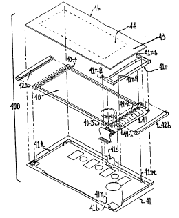
A second embodiment of the present invention is
illustrated in Figures 4 and 5A-5D. Mounting structure
400 of the second embodiment comprises horizontal plate
46. Horizontal plate 46 includes frame 43 surrounding a
transparent sheet 44. Transparent sheet 44 may be a
separate piece securely joined at its outside perimeter to
the inside perimeter of frame 43. Alternatively, frame 43
and transparent sheet 44 may be simply parts of a single
horizontal plate 46. Frame 43 is preferably opaque to
hide electronic components below and preferably includes
markings related to information to be displayed by an LCD
40. Mounting structure 400 further comprises resilient
shock mounts 42a, 42b which are preferably placed along
the two shorter edges of LCD 40 according to the second
embodiment. Resilient shock mounts 42a, 42b are made from
a low durometer material, preferably silicone rubber
having from 30 to 40 durometer, and are illustrated in
Figures 5A-5D.
Referring to Figures 5A-5D, resilient shock mounts
have first shock mount shape 42a and second shock mount
shape 42b. The shape of shock mounts 42a and 42b differ
because shock mount 42b must accommodate printed and
flexible circuitry 49 which is attached to edge 40-3 of
LCD 40, as illustrated in Figure 5C. Moreover, shock
mounts 42a and 42b must conform to the shape of housing
41, as illustrated in Figure 5D.
As illustrated in Figure 7, housing 41 comprises
sides 41d-g, wherein side 41d is opposite to 41e and side
41f is opposite to 41g. Sides 41d-f have two thicknesses,
wherein a thicker tier 41d-f(-1) is adjacent to back wall
41a, while a thinner tier 41d-f(-2) extends from and is
, ~ ~ ' , . '-, . . . ~-
,, : . .. , . , " - ,.:, . .: ' ''' , , : . ' :
WO90/15359 2 0 5 5 4 7 4 PCT/US~D/D31~6 ~-
-- 8 --
adjacent to only thicker tier 41d f(-l).
Housing 41 further comprises recesses 41h in back
wall 41a. Recesses 41h have various shapes or
configurations and are located in back wall 41a to
accommodate protruding electronic circuitry (not shown) on
LCD 40. Recesses 41h may be machined in back wall 41a
after housing 41 is molded. Recesses 41h can be
incorporated into the molding process to eliminate this
machining step.
Housing 41 still further comprises protrusions 41j
located at the corners of housing 41. In the second
embodiment, two protrusions 41j-1 protrude internally from
side 41f adjacent to corner 41-3 and three protrusions
41j-2 protrude internally from side 41e adjacent to corner
41-3 also. Adjacent to corner 41-4, three protrusions
41j-3 extend from side 41e internally and two protrusions
41j-4 extend from side 41g internally. All protrusions
are integrally connected to back wall 41a and the thicker
tier 41e-1, 41f-1 of sides 41e and f, respectively. The
protrusions serve as pressure points which deform the
shock mount locally under load. They also serve to locate
the shock mount without adding undesirable thickness to
the housing walls. The height of each group of
protrusions is dictated by a sealing ledge 41k. Sealing
ledge 41k extends along the inner perimeter of housing 41
on all four sides 41d-g. Sealing ledge 41k receives
horizontal plate 46. Sealing ledge 41k is further away
from back wall 41a on side 41f than on side 41g which is
opposite to side 41f. Therefore, sealing ledge 41k is
slanted at an angle on opposite sides 41e and 41d defined
by the height of sealing ledge 41k on sides 41f and 41g.
Referring to Figure 5A, shock mount 42a is applied to
edge 40-4 (see Figure 4) of LCD 40. A bottom membrane
42a-3 made of the same resilient material extends from end
42a-1 to end 42a-2 of shock mount 42a. Bottom membrane
42a-3 is thicker at end 42a-1 than at end 42a-2, thereby
leaving clearance for electronic components under LCD 40
. - ~ ~ , ~ , ,,
: . . , : , . , . , ~ . :,. : -
2 ~ ~ 5 ~1 7! ~ ,t
W~9~/15359 ~i ~ ; PCT/US90/03106
_ 9 _
and ~llowing the front surface of LCD 40 to be at an angle
with respect to housing 41. Both ends 42a-1 and 42a-2
have a wrap around configuration 42a-4 and 42a-5 an~ a
thin sheet of resilient material forming top membrane 42a-
6 which extends from oppositely extending wrap arounds
42a-4 and 42a-5. Shock mount 42a has a rear wall 42a-7
extendin~ from end-to-end (42a-1 and 42a-2) adjacent to
top membrane 42a-6 and bottom membrane 42a-3. opposite to
rear wall 42a-7 is an opening 42a-8 which exposes the
cavity or receptacle for edge 40-4 of LCD 40. Wrap around
configurations 42a-4 and 42a-5 are sized to receive corner
portions of edge 40-4 of LCD 40. Located on the top of
wrap arounds 42a-4 and 42a-5 are ribs 42a-9. Ribs 42a-9
protrude out from shock mount 42a. Ribs 42a-9 function as
pressure points when shock mounts 42a are compressed
during assembly.
Referring to Figure 5B, shock mount 42b is similar to
shock mount 42a except that bottom membrane 42b-3 has been
cut away so that it no longer extends from end-to-end
(42b-1, 2). Bottom portions 42b-31 and 42b-32 are located
only at ends 42b-1, 2 and form part of wrap around
configurations 42b-4 and 42b-5. Moreover, rear wall 42b-7
is adjacent to top membrane 42b-6 and extends from
end-to-end, but is adjacent to respective bottom portions
42b-31, 32 only at ends 42b-1, 2. Shock mount 42b is
shaped as described above to accommodate the associated
circuitry 49 at edge 40-3 of LCD 40, as illustrated in
Figure 5C. As shown in Figure 5D, shock mount 42a is
installed on LCD 40 so that bottom membrane 42a-3 contacts
the back wall 41a of housing 41. The thicker end of shock
mount 42a (end 42a-1, see Figure SA) is placed against a
thicker edge 41-2 of housing 41 so that LCD 40 is raised
up from back wall 4la and is essentially at an angle to
the back wall 41a of housing 41, as illustrated in
Figure 5D.
~ embranes 42a-6 and 42b-6 serve to maintain an air
gap between the LCD and transparent sheet 44, to avoid
:: :: . : . . . : .:~ ., . .: .. : :- ,: , - . :, , : . -
W090t15359 ~t PCT/U590/03106
~ ,.
-- 10 --
optical interference in the LCD ~iewing area.
~ When mounting structure 400 of the second embodiment
is assembled, shock mounts 42a and 42b are mounted onto
edges 40-4 and 40-3 of LCD 40, respectively. The
associated electronics are already assembled to LcD 40, as
illustrated in Figure 4. Edge 40-4, having shock mount
42a attached thereto, is placed within housing 41 so that
rear.wall 42a-7 and ends 42a-1,2 of shock mount 42a are
received by protrusions 41j located at the corners of
lO housing 41. Edge 40-3 and the associated electronics 49 ;
are placed into housing 41, and a bracket 41r (see
Figure 8) is placed over the associated electronics to
hold the electronics and edge 40-3 in place.
Bracket 41r has four sides preferably designed to
outline the edges of the associated electronics 49 on edge
40-3 of LCD 40. Referring to Figure 8, one side 41r-1 of
bracket 41r has extension 41r-5 comprising end piece 41r-6
for cooperating with receptacle 41m in back wall 41a of
housing 41. Extension 41r-5 also comprises a portion of
sealing edge 41k from side 41f of housing 41. Another
side 41r-3, opposite to side 41r-1, has an extension 41r-7
comprising end piece 41r-8. Hexagonal hole 41r-8a in end
piece 4lr-8 provides a locking interference fit when
pressed onto cylindrical post 4ln in back wall 4la. T~b
41r-4-a fits into an undercut (not shown) in housing side
wall 41-d, which combines with post 41n to positively lock
bracket 41r over LCD electronics 49 and into housing 41.
Side 41r-4 has hook 41r-9 extending internally away from
side 41r-4 and downward. Hook 41r-9 is received by
printed circuitry 49 in hole 49-1. Moreover, side 41r~4
comprises additional portions of sealing edge 41k from
side 41d of housing 41. Side 41r-2, which is opposite to
side 41r-4, has semi-circle-shaped cylindrical bosses
41r-lO which protrude internally from side 41r-2. Bosses
41r-lO function to allow easier removal of part 41r from
the mold used during injection molding of part 41r. Side
41r-2 bridges over flexible circuitry 49-2 to hold shock
W~ 90/15359 ~ 5 5`~ ; PCT/US90103106
-- 11 --
mount 42b and LCD edge 40-3 in place.
sracket 41r locks with housing 41 at at least points
41r-6, 41m and 41r-8a, 41n to hold edge 40-3 of LCD 40
within housing 41.
~ Horizontal plate 46 (Figure 4) is placed over LCD 40
in housing 41. The outer perimeter of horizontal plate 46
rests on seali~g edge 41k of housing 41 and bracket 41r~
Horizontal plate 46 is attached, preferably ultrasonically
welded to housing 41 at sealing edge 4lk and to bracket
41r at four sealing edges 41k-1, 41k-2, 41k-3, 41k-4. The
second embodiment can be hermetically sealed and evacuated
prior to hermetic sealing as described above for the first
embodiment also. A three-dimensional rigid box is created
by the combination of horizontal plate 46, housing 41 and
sides 41d-g of housing 41 after plate 46 is welded onto
housing 41.
The third embodiment of the LCD mounting structure is
illustrated in Figures 6A-6E. LCD mounting structure 600
comprises housing 61 which has upwardly extending sides
61d-g and screw receiving holes 61a-1 integrally
associated with back wall 61a of housing 61. Figure 6B
illustrates the inside of housing 61. Sides 61f and 61g
are opposite to each other and side 61f is adapted to
receive latch 61c while side 61g is adapted to form
hinge 61b which will receive a hinge pin.
Resilient shock mounts 62a,b are mounted on the edges
60-4,3 of an LCD 60, respectively, as illustrated in
Figure 6C. Shock mounts 62a,b are similar to the shock
mounts 42a,b of the second embodiment. Also shown in
Figure 6C is row driver printed circuitry 69 and flexible
cable 69a associated with edge 60-3 of LCD 60.
LCD 60, associated circuitry, and shock mounts 62a,b
are held within housing 61 by LCD frame 63. Referring to
Figure 6D, LCD frame 63 is a horizontal plate having an
3S inside perimeter and an outside perimeter. The inside
perimeter defines a display window 63a and is shaped with
a flange. Frame portion 63b is wider than portions 63c-e
.. ,, : ,: . : ,", . . . . .
WO90/15359 2 0 5 ~ ~ 7 4 ` PCT/US90/03106
12 ~ `
so that row driver printed circuitry 69 is hidden from
- view when LCD frame 63 is mounted over LCD 60 in housing
61. LCD frame 63 also comprises through-holes 63f near
the four corners of LCD frame 63. Through-holes 63f
receive screws 64. Screws 64 connect LCD frame 63 to
housing 61 after LCD 60 is placed in housing 61.
Figure 6E illustrates overlay 65 which preferably provides
the logo information and display symbols for LCD 6~.
Overlay 65 can be made of plastic, preferably
polycarbonate, and has an inner perimeter defining a
window 65a. One side of overlay 65 has an adhesive
applied. The adhesive side of overlay 65 adheres to LCD
frame 63 after assembly. After assembly, overlay 65
covers screws 64. Mounting structure 600 is assembled by
aligning LCD 60, having resilient shock mounts 62a,b
mounted on the edges thereof, inside housing 61 as
illustrated in Figure 6A. LCD 60, associated circuitry,
and shock mounts 62a,b fit within an area defined by screw
receiving holes 61a-l. A bracket similar to bracket 41r
may be placed over circuitry 69 and its associated
flexible circuitry (not shown) to hold circuitry 69 in
place in housing 61. Alternatively the retaining features
of bracket 4lr may be incorporated in the rear surface
shape of LCD frame 63. LCD frame 63 is placed over LCD 60
and the associated parts and screws 64 are inserted to
attach LCD frame 63 to housing 61, thereby enclosing LCD
60 and the associated parts within. After screws 64 are
inserted, overlay 65 is adhered to LCD frame 63. A rigid
three-dimensional box is created according to the third
embodiment by the cooperative effects of housing 61, LCD
frame 63 and screws 64. The third embodiment has the
advantages of allowing disassembly and repair of the LCD
and associated electronics, or replacement of plastic
parts. This will improve production yield and reduce unit
cost. A non-glare film 60c applied to LCD 60 functions as
the transparent sheet 44 of Figure 4 so that the display
can be viewed and the LCD simultaneously protected.
.. . . . . :
.- ,.
W~ 0/15359 ZO ~ ;71~ PCTtUS90/03106 -
- 13 -
Installing the LCD with no cover sheet increases display
contrast and readability, eliminates optical interference
- problems, and prevents accidental trapping of moisture or
foreign material in the viewing area. LCD frame 63 having
window 63a frames-LCD assembly 60 to create a display
window.
Nounting structures lO0 (first embodiment), 400
~second embodiment), and 600 ~third embodiment) allow the
LCD glass plates to float with respect to the housing.
The housing may be deformed or otherwise stressed by
dropping or compressing its associated portable computer,
but the LCD glasses remain relatively flat and cushioned
from the shock and load. Effectively, the mounting
structures suspend the LCD glasses, and leave the glass
more nearly planar when the housing is deformed. The
effectiveness of mounting structure 400 was tested by
dropping two prototype portable computers having the
second embodiment of the present invention incorporated
therein from a height of ten feet onto concrete several
times. The LCD assemblies survived the drops without
damage. It was found that while the LCD assemblies of the
first embodiment survived the impact of this test also,
the shock mounts 2 of the first embodiment did not remain
in place after repeated testing. The second and third
embodiments were designed to overcome this problem. Shock
mounts 42a,b and 62a,b extend from one corner to another
corner along respective edges 40-4,3 and 60-4,3. In
another test, the portable computer containing the
invention was compressed by having a user sit on chairs of
various types while the computer was in the user's back
pocket (a potential mishap likely to occur with pocket
sized portable computers), thus applying stress to the
computer housing. An inspection of the portable computer
after the compression test revealed no damage to the LCD
assembly. The LCD mounting structures, according to all
above embodiments, are designed to absorb the shock
associated with dropping or other day-to-day handling of a
. .:
.
W O 90/15359 20~547`,~ PC~r/US90/03106. ~ .
~ ~ , .
- 14 - -'
portable computer and thereby protects the LCD.(glass and s
circuitry) from damage. ~ -
While particular embodiments of the present invention
have been shown and described, it will be obvious to those ¦ :
5 skilled in the art that changes and modifications may be I .
made without departing from this invention in its broader
aspects. For example, although embodiments having two and
four shock mounts are shown, another embodiment ha~ing a
single shock mount extending around the perimeter of the
lo LCD assembly could also be made. Therefore, the appended
claims are to encompass within their scope all such
changes and modifications as fall within the true spirit
and scope of this invention.
.. . . :
. . - :
.: :. . : ,: .: . ~ :
.. : . . .: