Note: Descriptions are shown in the official language in which they were submitted.
BC9-90-053 1 2~555~
MULTIMEDIA SYSTEM
Background of the Invention
The present invention relates to multimedia computer
systems.
Multimedia computer systems are information handling
systems which combine the information handling
characteristics of traditional computer systems with high
quality video and audio presentations. The video
presentation is provided by a video display device and
the audio presentation is provided by an audio output
device.
Multimedia computer systems include media sources
which generate media signals. The media signals include
audio signals, which are provided to the audio output
device, and image signals, which are provided to the
video display device. The image signals may include
graphics signals, text signals, animation signals and
full motion video signals. An image signal is converted
to a video presentation by the display device, which
receives the image signal and scans the image signal in a
raster pattern across a screen of the display device.
The speed with which the display device scans the image
is called the sweep rate. The screen has a horizontal
resolution and a vertical resolution which define display
device screen coordinates. The presentation from one
complete scan of the screen is called a frame. To
provide a full motion video presentation, a display
device generates multiple frames per second.
It is often desirable to concurrently display a
plurality of different image signals, including full
motion video signals, via a single video display device.
The image signals may be concurrently displayed by the
display device using a plurality of different methods.
Multiple image signals may be concurrently displayed
using a multiple plane method. With the multiple plane
method, a background signal which is rapidly changing
(e.g., full motion video) is stored in a first memory
(the background memory) to provide a background plane. A
BC9-90-053 2 205555~
foreground signal which is relatively constant (e.g.,
text or graphics) is stored in a second memory (the
foreground memory) to provide a foreground plane. The
two planes are merged and a merged signal is provided to
the display device.
Multiple image signals may be concurrently displayed
using an overlay method. With the overlay method, a
frame of a full motion video signal is provided to a
memory such as a frame buffer which stores the full
motion video frame as a background frame. An overlay
image signal is then stored in a portion of the memory
thereby over writing the full motion video signal that is
stored in that portion of the memory. The entire frame
is then read from the memory to provide an overlaid image
signal to the display device.
Multiple image signals may be concurrently displayed
using a color keying method. With the color keying
method, a first image signal is provided to control logic
as a background frame. A second image signal which
includes portions having a designated color is provided
to the control logic as a key frame. For normal color
keying, the control logic provides the key frame to the
display device unless the designated color is present, at
which time the control logic provides the background
frame. Bowker et al., U.S. Patent No. 4,599,611,
discloses a computer system which uses the color keying
method. In Bowker et al., two image signals (a set
containing text signals and a set containing graphics
signals) are supplied to a switch which receives the
image signals and provides an output to a video display
device on a pixel by pixel basis based upon whether a
predetermined color is present. Prior to being provided
to the switch, the image signal is converted to RGB
(Red/Green/Blue) format if not already so encoded.
Multiple image signals may be concurrently displayed
using a window method. With the window method, a first
image signal (e.g., a full motion video image signal)
provides a background image plane which is stored in a
memory such as a frame buffer. A second image signal
(e.g., a text or graphics image signal) provides a second
2055~5~
BC9-90-053 3
image plane which is stored in all but a portion of the
memory. This portion is a void, i.e., a window, in which
the background image plane remains. This windowed image
signal is then provided to the display device.
A window is a rectangular area in which the
background image signal is displayed. The window is
defined by window coordinates which define the location
and size of the window with respect to display device
screen coordinates. Multiple windows are often
concurrently presented on a single display device.
During concurrent display, one window, usually the most
visible window, is the active window.
It is known to display windows of non-full motion
video image signals using a system in which a digital bus
connects a plurality of window modules to a display
controller. The display controller connects the display
bus to a system display. Colley, Martin,
"Parallel-Architecture Windowing Display" Department of
Computer Science, University of Essex, Wivenhoe Park,
Colchester, Essex, U.K. (1987) discloses such a system.
In Colley, the window modules are provided by
dividing a display memory into physically separate window
areas. Each image signal window is maintained in its
entirety in a respective window module; the visibility of
overlapping portions of the windows is determined via
arbitration as the screen of the display device is
updated. Each window module contains a window management
unit which defines the size, position and arbitration
priority of an associated window.
The display controller reads data in 8 or 16-bit
words from the display memories via the display bus. The
data are read from each display memory via the digital
bus to allow the memory to adequately provide information
for display. The information which is read from the
different display memories is stored in a frame buffer.
The frame buffer is read to provide an image signal to
the display device.
BC9-90-053 4 2~555 S~
Summary of the Invention
It has been discovered that a plurality of image
signals, including full motion video image signals, may
be concurrently displayed in real time using system which
includes a media bus which composes the image signals in
real time. Such a system advantageously allows real time
composition and display of image signals without video
memory.
The invention features an information handling
apparatus for transferring and composing image signals.
The apparatus includes a plurality of media sources which
provide a corresponding plurality of image signals, a
media bus connected to the media sources, and a media
control module coupled to the media bus. The media bus
allows selective access for the plurality of image
signals; the selective access enables composition of the
independent image signals in response to control
information. The media control module receives a
composed image signal from the media bus and provides the
composed image signal to a display device.
In preferred embodiments the apparatus includes one
or more of the following features: the media control
module generates the control information for permitting
composition on the media bus of the plurality of image
signals;
the composition includes allowing selective access
of the image signals on a point by point basis; each
image signal represents a virtual screen of information;
the apparatus further includes a plurality of media bus
interface circuits corresponding to the plurality of
media sources, each media bus interface circuit being
configured to allow the selective access to the media bus
for a respective media source; the display device
presents the composed image at a predetermined
presentation speed, the composition of the independent
image signals occurs in real time, and real time is
defined with reference to the predetermined presentation
speed; the apparatus further includes a system bus
BC9-90-053 5 2 :~ $ 5~ ~
connected to the plurality of media sources, the system
bus being configured to transport input/output
information between the plurality of media sources; the
plurality of media sources include a processor module
which provides image signals; the plurality of media
sources includes a programmable receiver module which
receives full motion video transmissions and generates
full motion video signals; the full motion video
transmissions are provided by an analog full motion video
source; and, the full motion video transmissions are
electromagnetic transmissions provided by a remote
transmitter.
Other features of the invention will be apparent
from the following description of the preferred
embodiment and from the claims.
Brief Description of the Drawings
Fig. 1 is a block diagram of a multimedia system
according to the present invention.
Fig. 2 is an example of a composed frame.
Fig. 3 is a block diagram of a media control module
and an audio module of the Fig. 1 multimedia system.
Fig. 4 is a block diagram of a video processor
circuit of the media control module of Fig. 3.
Figs. 5A and 5B are a block diagram of the Fig. 4
video processor circuit.
Fig. 6 is a block diagram of a synchronization
circuit of the media control module of Fig. 3.
Figs. 7A and 7B are a block diagram of the Fig. 6
synchronization circuit.
Fig. 8 is a block diagram of a bus interface circuit
of the Fig. 1 multimedia system.
Fig. 9 is a schematic block diagram of a window
control circuit of the Fig. 5 bus interface circuit.
Fig. 10 is a schematic block diagram of a window
priority circuit of the Fig. 7 window control module.
Figs. llA and llB are a schematic block diagram of a
receiver/switch circuit of the Fig. 8 bus interface
circuit.
BC9-90-053 6 205555~
Detailed Description
Multimedia System
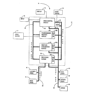
Referring to Fig. 1, multimedia system lO includes
multimedia core 12, display device 14, which may be for
example an all points addressable (APA) video graphics
array (VGA) or high definition television (HDTV) display
device, audio output device 15, which may be for example
speakers or headphones, input device 16, which may be for
example a keyboard or a mouse, and analog full motion
video source 17, which may be for example, a video tape
player or a video disk player. Multimedia core 12 is
arranged in modules; information is transferred among
modules via system bus 20 and media bus 24. Information
is provided to and received from multimedia core 12 via
small computer system interface bus (SCSI) 22 and storage
bus 23.
Multimedia core 12 includes media control module 30
and may include audio module 31, graphics accelerator
module 34, processor module 36 and programmable receiver
module 38. Modules 34, 36, and 38, which are media
sources (i.e., devices which provide media signals), are
each connected to media bus 24 via media bus interface
circuits 39a, 39b, 39c, respectively. (Media bus
interface circuits 39a, 39b, 39c are referred to
generally as bus interface circuit 39.) Image signals
from the media sources selectively access media bus 24 in
response to control information; the selective access
allows real time composition of the image signals. Audio
signals from the media sources selectively access media
bus 24 in response to control information; the selective
access allows real time composition of the audio signals.
A composed image signal is provided from media bus
24 to display device 14 via media control module 30; a
composed audio signal is provided to audio output device
15 via audio module 31. All input information from input
device 16 is received via media control module 30.
Programmable receiver 38 receives analog full motion
video input information directly from video source 17;
2055554
BC9-90 053 7
programmable receiver 38 may also receive electromagnetic transmissions from
remote transmitters (e.g., television transmissions from television studios). The
configuration of multimedia system 10 and of multimedia core 12 is meant to be
representative; it is understood that the system and core configurations may be
changed to satisfy a user's needs.
System bus 20 conforms to a conventional input/output bus architecture
such as the IBM~ Micro Channel~ Architecture or the IBM Family I (i.e., IBM
AT~) bus architecture. System bus 20 is connected between modules which
transfer input/output information such as media control module 30, graphics
accelerator module 34, processor module 36 and programmable receiver module
38.
SCSI bus 22, which conforms to a conventional SCSI bus architecture,
functions as a block transfer bus via which large bloclcs of information are
transferred,. SCSI bus 22 is connected directly to modules which require the
transfer of large quantities of information such as processor module 36 and
graphics accelerator module 34 as well as to SCSI devices 40 (e.g., a SCSI tape
drive, a SCSI read~write optical disk device, or a SCSI CDROM reader). Because
SCSI bus 22 is directly connected to modules which require transfers of large
quantities of information, this information need not be transferred from SCSI bus
22 to modules which require the SCSI information via system bus 20.
Accordingly, system bus 20 is free to perform other types of transfers.
Storage bus 23 conforms to a conventional storage bus architecture. Storage
bus 23 is connected directly between devices 41 which store information (e.g., a 3
1/2 inch disc drive, a hard drive or the lilce) and processor module 36.
Media bus 24 conforms to a media bus architecture which is defined herein.
Media bus 24 is connected between media control module 30, audio module 31
and media bus interface circuits 39 of media sources such as graphics accelerator
module 34, processor module 36 and programmable receiver module 38.
20~5~
BC9-90-053 8
By providing system bus 20, media bus 24 and SCSI
bus 22, multimedia system 10 functions as a balanced
system. Each bus optimally transfers the type of
information for which it is designed. Accordingly,
contention problems that arise when a bus must transfer
information for which it is not designed are avoided.
Media core 12, and more specifically media bus 24,
composes image signals in real time for display by
display device 14. In other words, media core 12
combines image signals in parallel in real time on a
point by point basis for display by display device 14.
For the purposes of this application, "real time" is
determined with reference to the sweep rate of display
device 14, i.e., the speed with which information is
presented by display device 14. Accordingly, the speed
with which media bus 24 transmits information need only
be as fast as the sweep rate of display device 14.
An image signal is provided by a media source to
media bus 24 via a respective media bus interface circuit
39 on a point by point basis in response to control
information. A point is related to the resolution of
display device 14. Accordingly, if display device 14 is
a 640 by 480 VGA monitor, a point corresponds to a
coordinate of the VGA monitor. Alternately, if display
device 14 is a 1920 by 1035 HDTV monitor, a point
corresponds to a coordinate of the HDTV monitor.
A virtual screen implementation (i.e., every module
assumes that it is providing an image signal to a
display) is used by multimedia system 10 to achieve
application transparency. A virtual screen
implementation creates the appearance to each module of a
dedicated display device. Thus, each media source which
is generating an image signal generates that image signal
whether or not the media source is granted access to
media bus 24.
An image signal which is contained on media bus 24
is received by media control module 30 on a point by
point basis and is provided to display device 14 on a
point by point basis. The combination of the image
signals from the media sources on media bus 24 provides a
BCg-9O-053 9 20~55 1
composed image signal which is provided to media control
module 30. Media control module 30 adjusts the
attributes (e.g., the voltage level) of the composed
image signal to correspond to the attributes required by
display device 14 and drives an adjusted composed image
signal to display device 14. If no attribute adjustment
were required, it is possible to provide the composed
image signal directly to display device 14.
Referring to Fig. 2, an example of a composed frame
is shown. For the purposes of this example, display
device 14 is a VGA display device having a display
resolution of 640 columns by 480 rows. The image signal
which provides the background plane is provided by
processor module 36. An image signal which is displayed
in a first window (WINDOW 1) is provided by programmable
receiver 38; this image signal is a full motion video
signal. An image signal which is displayed in a second
window (WINDOW 2) is provided by graphics accelerator
module 34. The presentation of the composed frame is
determined by a user via input device 16; accordingly,
the presentation of the frame may he changed via input
device 16. It is understood that the example shown is
merely meant to be illustrative of the invention.
The example shown is for one frame of display device
14. This frame is repeated multiple times per second
thus allowing display device 14 to provide a full motion
presentation. Accordingly~ the following description of
a composition of a frame is repeated multiple times per
second.
During composition of the frame, bus interface
circuits 39 allow selective access to media bus 24 of
respective media sources in response to control
information. In the preferred embodiment, the control
information is provided by media control module 30. The
control information which is provided to bus interface
circuits 39 includes switching coordinate information as
well as window priority information. This control
information is provided when the frame is initially
composed and is maintained within bus interface circuits
39 until the information for a particular module changes.
20~S~
BC9-90-053 10
I.e., multiple frames may be composed from the same
switching coordinate information. If certain switching
coordinate information is modified (e.g., because the
display area of a particular module changes) then the
modified switching coordinate information is provided to
the appropriate bus interface circuit 39. This modified
switching coordinate information is substituted within
the appropriate bus interface circuit 39.
Synchronized media sources drive media bus 24 in
real time. Image signals are received by media control
module 30 in real time. Thus for sources which are
synchronized, there is no need to store information
within video memory on media control module 30 before
displaying the information via display device 14.
Accordingly, the image signals that are contained on
media bus 24 provide a composed image which is a single
plane. Unsynchronized media sources provide image
signals to media control module 30, which synchronizes
these signals via a frame buffer prior to display.
Composition of the frame shown in Fig. 2 is
initiated by bus interface circuit 39b granting processor
module 36 access to media bus 24 based upon the window
priority and switching coordinate information. Processor
module 36 provides an image signal to media bus 24 until
display device 14 reaches coordinate Hl,V1. At this
location, bus interface circuit 39b rescinds the access
grant to media bus 24 of processor module 36 and
simultaneously, bus interface circuit 39c grants
programmable receiver module 38 access to media bus 24.
Programmable receiver module 38 provides an image
signal to media bus 24 until display device 14 reaches
coordinate H2,V1, at which location bus interface circuit
39c rescinds the access grant to media bus 24 of
programmable receiver module 38 and bus interface circuit
39b grants processor module 36 access to media bus 14.
Access to media bus 24 continues to be interchanged
between processor module 36 and programmable receiver
module 38 at the horizontal coordinates Hl and H2 until
display device 14 reaches coordinate H2,V2.
BC9-90-053 11 205~
At coordinate H2,V2, bus interface circuit 39c
rescinds the grant of access to media bus 24 of
programmable receiver module 38 and bus interface circuit
39a grants graphics accelerator module 34 access to media
bus 24. Graphics accelerator module 34 provides an image
signal to media bus 24 until location H3,V3, at which
location access to media bus 24 is switched to processor
module 36 by bus interface circuits 39a, 39b, 39c.
Access to media bus 24 continues to be exchanged between
processor module 34, programmable receiver module 38, and
graphics accelerator module 34 at the horizontal
coordinates H1, H2 and H3 until display device 14 reaches
coordinate H4,V3.
At coordinate H4,V3, programmable receiver 38 has
completed its contribution to the composition of the
screen to display device 14. Accordingly, for the
remainder to the screen, programmable receiver 38 is no
longer granted access to media bus 24.
At horizontal coordinates H3 and H4, access to media
bus 24 is switched between processor module 36 and
graphics accelerator module 34 until display device 14
reaches coordinate H3,V4. At coordinate H3,V4, access to
media bus 24 is returned to processor module 36 for the
remainder of the frame.
Media Bus Architecture
Media bus 24 serves as the pathway for media signals
defined by the media bus architecture. The media bus
architecture defines media signals for transfer of
information between media sources and media control
module 30. The media signals include image signals,
control signals and audio signals. Accordingly, media
bus 24 includes a plurality of video channels, a media
control channel (MCC) and an audio channel. The video
channels include a primary video channel (PVC), a
secondary video channel (SVC), and a digital video
channel (DVC).
The primary video channel is the channel via which
image signals from the media sources are composed to
20~55~
BC9-90-053 12
provide a primary composed image signal to media control
module 30. The primary channel includes paths for a
primary analog image signal having red green and blue
components (PVC RGB), a primary color key match (PVC CKM)
signal, and a primary arbitration signal (PVC ARB). The
PVC RGB signal is a differential analog RGB signal which
is driven directly onto the primary channel by the media
sources as an analog waveform under control of media
control module 30. The PVC CKM signal controls video
switch multiplexing in media control module 30; the PCKM
signal is driven active low at pixel rates coincident
with RGB data. The PVC ARB signal is a 4-bit one of
sixteen priority arbitration signal.
The secondary video channel is the channel via which
alternate or additional image signals from the media
sources are composed to provide a secondary composed
image signal to media control module 30. The secondary
channel includes paths for a secondary analog image
signal having red, green and blue components (SVC RGB), a
secondary color key match (SVC CKM) signal, and a
secondary arbitration signal (SVC ARB). The SVC RGB
signal is a differential analog RGB signal which is
driven directly onto the secondary channel by the media
sources as an analog waveform under control of media
control module 30. The SVC CKM signal controls video
switch multiplexing in media control module 30; the SVC
CKM signal is driven active low at pixel rates coincident
with RGB data. The SVC ARB signal is a 4-bit one of
sixteen priority arbitration signal.
The digital video channel is the channel via which
digital video signals are transferred from a media source
to media control module 30. The digital video channel is
capable of supporting high-speed live video transfers as
required by HDTV and other high resolution displays as
well as transfers from other digital video sources. The
digital video channel includes paths for a 32-bit image
signal (DIG IM), a digital clock signal, a digital HSync
signal and a digital VSync signal. The DIG IM signal
includes an active high 8, 16, or 24-bit RGB signal, plus
an 8-bit Alpha signal, which represents a degree of
2~5~
BC9-90-053 13
transparency. The digital clock signal is provided by
media control module 30 to clock data either through
media control module 30 to the media control module RGB
output terminals or into a frame buffer of media control
module 30. The maximum clock frequency of the digital
video channel is 80 MHz, thus supporting HDTV data rates
of 74.25 MHz.
The media control channel provides paths for media
control information which controls the transfer of
information over media bus 24. The media control channel
allows media control module 30 to issue device-specific
control information as well as to broadcast global
control information to all media sources. The media
control information includes window control block data
which are written to each adapter as well as vital
product data and personality data which are read from
each adapter when system 10 is initialized. The media
control channel also includes paths for a source
synchronization signal (SOURCE SYNC) and a system
synchronization signal ~SYS SYNC) as well as a window
clock signal (WINDOW CLK). The media control channel
also includes a path for a global reference signal (V
BIAS) which is provided to all media sources which are
connected to media bus 24.
The audio channel includes paths for a high fidelity
digital audio signal (AUDIO) as well as a telephony grade
digital (TEL AUDIO).
Media Control Module
Referring to Figs. 1 and 3, media control module 30
provides a plurality of functions for media core 12.
Media control module 30 controls composition on media bus
24. Media control module 30 also functions as a receiver
and level converter for an image signal which is received
from the primary video channel, the secondary video
channel or the digital video channel. Media control
module 30 also functions as a composition facility for
image signals. Media control module 30 also functions as
a video mixer for mixing image signals from the primary
BC9-90-053 14 20~5~S~
video channel, the secondary video channel and the
digital video channel as well as image signals which are
generated internally by media control module 30. Media
control module 30 also functions as an image capture
facility for storing images from a media source. Media
control circuit 30 also functions as a display device
driver circuit. Media control module 30 also functions
as a synchronization signal generator for generating the
synchronization signals for media core 12. Media control
module 30 also functions as a composition facility for
audio signals. Media control module 30 also provides,
via input device 16, a direct user interface. Media
control module 30 also interfaces with system bus 20 and
SCSI bus 22. Some of the functions which media control
module 30 performs occur continuously, other functions
occur as needed. However, a plurality of functions can
occur simultaneously.
Media control module 30 receives continuous data
streams across the video channels of media bus 24 while
controlling the media sources via the media control
channel. Media control module 30 includes media control
circuit 50, bus interface circuit 51, image signal
processor circuit 52, and frame capture circuit 54, all
of which are connected via media control module bus 55.
Media control module 30 also includes display device
adapter circuit 56 and synchronization generator circuit
58.
When controlling composition of image signals on
media bus 24, media control module 30 uses media control
circuit 50. Media control circuit 50 includes media
control module microprocessor 62, memory controller 64,
media system memory 66, which may be dynamic random
access memory (DRAM), and menu memory 68, which may be an
electronically erasable programmable read only memory.
Media system memory 66 holds a media control module
operating system which controls the functions of media
control module 30; memory 66 also contains I/0 handling
information for interfacing with input device 16. Menu
memory 68 stores menu information which may be accessed
via input device 16 (e.g., pull-down menus which are
BC9-90-053 15 20~5~
accessed via a pointing device such as a mouse). Media
control module microprocessor 62 accesses media system
memory 66 and menu memory 68 via memory controller 64.
Memory controller 64 and bus interface circuit 51 also
control access to any memory which may be resident on a
particular bus interface circuit 39. E.g., if a new
module is added to media core 12, media control module 30
requires media source personality data which are stored
in the bus interface circuit 39 of the new module. The
media source personality data are passed in a personality
block via the media control channel 30 to system memory
66 under control of memory controller 64. The
personality data are used by media control module
microprocessor 62.
Composition of a frame is initiated by a user
defining composition characteristics via input device 16.
The composition characteristics may include the desired
size and shape of a window via which the image signal for
a particular media source is to be displayed. Media
control module microprocessor 62, in conjunction with the
I/0 handling information which is stored in media system
memory 66, receives the user defined composition
characteristics. Media control module microprocessor 62
then generates control information such as switching
coordinate information and window priority information
which is transmitted via the media control channel of
media bus 24 to the media sources which are connected to
media bus 24. The media sources are granted selective
access to media bus 24 based upon this control
information.
When functioning as a receiver and level converter
or when functioning as a video mixer, media control
module 30 uses image signal processor circuit 52. Image
signal processor circuit 52 includes display controller
70 as well as mixer circuit 72. Display controller 70
functions as a interface circuit between frame capture
circuit 54 and mixer circuit 72 because, by using frame
capture circuit 54, media control module 30 may function
as a source of an image signal. In addition to
functioning as an interface between frame capture circuit
20~5~
BC9-90-053 16
54 and mixer 72, display controller 70 also manages
acquisition and display of images which are stored in
frame capture circuit 54. Display controller 70 also
manages other display functions such as background color
flood in which the background presentation of display
device 14 is set to a certain color. Display controller
70 also controls the fade level of selected frame buffer
images (e.g., the menu image or a captured image) under
control of media control module microprocessor 62.
When functioning only as a receiver and level
converter, mixer circuit 72 of image signal processor
circuit 52 receives either the PVC RGB signal, the SVC
RGB signal or the DIG IM signal from media bus 24. Mixer
circuit 72 levels the received image signal to provide a
composed image signal (COMP RGB) which has a constant
base output level, e.g., a constant black level.
When functioning as a leveling circuit and a mixer
circuit, mixer circuit 72 of image signal processor
circuit 52 receives one or more of the PVC RGB and PVC
CKM signals, the SVC RGB and SVC CKM signals, and the DIG
IM signal from media bus 24, as well as a capture signal
(MCM RGB) from frame capture circuit 54. Mixer circuit
72 mixes these signals under control of display
controller 70 and levels the mixed signal to provide the
COMP RGB signal.
When functioning as a composition facility, media
control module 30 uses mixer circuit 72 in conjunction
with media control circuit 50. During composition within
media control module 30, mixer circuit 72 switches on a
point by point basis between the PVC RGB, SVC RGB and DIG
IM signals as well as a frame capture signal which is
provided by frame capture circuit 54 to provide the COMP
RGB signal. Display controller 70 controls the switching
based upon information which is provided by media control
circuit 50. Media control circuit 50 provides this
information in response to user defined composition
characteristics.
When functioning as an image capture facility, media
control module 30 uses frame capture circuit 54. Frame
capture circuit 54 includes frame buffer control circuit
BC9-90-053 17 2055~
78, frame buffer 80, which is video random access memory
(VRAM), switch circuit 82 and fader circuit 84. Switch
circuit 82 includes image switch 86, analog to digital
(A/D) converter 88 and buffer circuit 90. Fader circuit
84 includes digital to analog converters 92, 94 and fader
circuit 96. Frame capture circuit 54 receives the
synchronization signals PVC SYNC, the SVC SYNC, the SYS
SYNC. Frame capture circuit 54 also receives the PVC RGB
signal, the SVC RGB signal and the DIG IM signal from
media bus 24 and a composed image signal from image
signal processor circuit 52 and selectively stores one of
these signals in response to control information which is
provided by media control module microprocessor 62 via
media control bus 55 to capture a frame of information.
When storing the frame capture signal, frame capture
circuit is synchronized by the synchronization signal.
Frame capture circuit 54 may provide to image signal
processor circuit 52 the analog equivalent of the capture
signal as the MCM RGB.
Frame capture circuit 54 is used to capture images,
to receive image signals from non-genlocked (i.e.,
unsynchronized) sources and to provide menu information.
Accordingly, frame buffer 80 includes both an image
capture plane as well as a menu plane. The image capture
plane is capable of storing four captured images. The
menu capture plane is capable of storing menu information
which is received from menu memory 68.
When capturing an image, image signals are
selectively provided to frame buffer 80 via switch 86.
The analog image signal is converted to an equivalent
digital signal via analog to digital converter 88 prior
to being provided to switch 86; the switched image is
buffered via buffer 90. Buffer 90 is used to synchronize
information which is provided to frame buffer 80 because
the information may not be genlocked (i.e., synchronized)
or may have timing skews due to composition or bus
transmission. Image signals are provided to frame buffer
80 via serial ports. When writing to frame buffer 80,
frame buffer 80 is synchronized with the source of the
BC9-90-053 18 205555~
information. When reading from frame buffer 80, frame
buffer 80 is synchronized with the SYS SYNC signal.
When presenting menu information, menu information
which is stored in menu memory 68 is provided, via media
control module bus 55, to a random access port of frame
buffer 80 by media control module microprocessor 62. The
menu information is stored in the menu plane of frame
buffer 80. The menu information which is stored in the
menu plane is then presented via mixer circuit 72.
When functioning as a display device driver, media
control module 30 uses display device adapter circuit 56.
Display device adapter circuit 56 includes 75 ohm driver
circuit 98 and RGB to NTSC converter circuit 100.
Display device adapter circuit 56 receives the composed
image signal COMP RGB from image signal processor circuit
52 and the SYS SYNC signal from synchronization generator
circuit 58. Display device adapter circuit 56 generates
via 75 ohm driver circuit 98 an RGB signal (RGB OUT),
which is capable of driving a VGA monitor Display device
adapter circuit 56 generates via RGB to NTSC converter
circuit 102 a composite NTSC signal (NTSC OUT), which is
capable of driving a video monitor, video cassette
recorder or other device which requires a direct
composite baseband video input signal.
When functioning as a synchronization signal
generator, media control module 30 uses synchronization
generator circuit 58. Synchronization generator circuit
58 includes programmable sync generator 104 and
oscillator 106. Synchronization generator circuit 58
receives the SOURCE SYNC signal, which is received via
media bus 24 from a media source as selected by media
control module microprocessor 62, an external house
synchronization signal (EHS), which may be externally
provided to media control module 30, and an internal time
based oscillator signal (INT OSC) which is generated by
oscillator 106 of synchronization generator circuit 58.
The EHS signal may be a synchronization signal which
includes separate horizontal and vertical components (EHS
HSYNC, EHS VSYNC), a composite synchronization signal
(i.e., a single signal which includes both horizontal and
20555S~
BC9-90-053 19
vertical components) or a black burst synchronization
signal (i.e., a composite signal minus any video).
Synchronization generator circuit 58 provides the SYS
SYNC signal and the WIND CLK signal to the media control
channel as well as a master clock signal (MASTER), which
is the clock signal used internally by media control
module 30, a blanking signal (BLANKING), a media control
module synchronization signal (MCM SYNC), a display
synchronization signal (DISP SYNC) and an NTSC composite
synchronization signal (NTSC SYNC). The WIND CLK signal
is provided to all media sources, thus allowing
synchronous switching during composition. The MASTER
signal is the clock signal used internally by media
control module 30. The BLANKING signal, which includes a
horizontal blanking signal (H BLANKING) and a vertical
blanking signal (V BLANKING), controls when display
device 14 is not illuminated such as during the retrace
of a display device which scans an image signal. The MCM
SYNC signal, which includes a horizontal component (MCM
HSYNC) and a vertical component (MCM VSYNC), controls the
display timing for media control module 30. The NTSC
SYNC signal is the signal which is a synchronization
signal which is compatible with the standard U.S. NTSC
format. The DISP SYNC signal, which includes a
horizontal component (DISP HSYNC) and a vertical
component (DISP VS~NC), controls the horizontal and
vertical synchronization pulses which VGA type display
devices require.
When functioning as a direct user interface, input
signals which are provided by input device 16 are
received by media control module microprocessor 62 via
media control module bus 55. These input signals may be
used to generate menu presentations, in which case the
input signals are used directly by media control module
30. These input signals may also be intended for another
module such as processor module 36, in which case the
input signals are received by media control module 30 and
then provided to processor module 36. When the input
signals are intended for another module, media control
module 30 still provides the necessary support to
BC9-90-053 20 20~55~
interpret the input signals before providing the input
signals to the appropriate module.
When interfacing with system bus 20 and SCSI bus 22,
media control channel 30 uses bus interface circuit 51.
Bus interface circuit 51 also allows media control
channel 30 to interface with the media control channel of
media bus 24.
Referring to Fig. 4, mixer circuit 72 uses switches
110, 112, 113, 114 to provide one or more of the PVC RGB
signal, the SVC RGB signal, the MCM RGB signal and the
RGB equivalent of the DIG IM image signal, respectively,
to summer circuit 116. Switches 110, 112, are controlled
by an inhibit primary video signal (INH PVC) and an
inhibit secondary video signal (INH SVC) which are
provided by display controller 70 and the PVC CKM and SVC
CKM signals which are provided by respective media
sources. Switches 113, 114 are controlled by the MCM SEL
and DIG SEL signals which are provided by display
controller 70. Summer circuit 116 receives the image
signals provided by switches 110, 112, 113, 114 and
generates the mixed, composed RGB image signal COMP RGB.
Summer circuit 116 also includes a bias generator circuit
117 which generates the reference voltage V BIAS.
The PVC RGB signal, which is received from media bus
24 by primary receiver circuit 118, is provided to summer
circuit 116 based upon the PVC CKM signal, which is
received from media bus 24, and the INH PVC signal, which
is provided by display controller 70. Switch 110
provides the PVC RGB image signal to summer circuit 116
when both the PVC CKM signal and the INH PVC are inactive
as determined by OR gate 119. OR gate 119 provides a
select primary channel (PVC SEL) to switch 110.
Accordingly, the PVC RGB signal is provided to summer
circuit 116 unless the primary video channel is inhibited
or a color key match corresponds to the PVC RGB signal
for the particular coordinate.
The SVC RGB signal, which is received from media bus
24 by secondary receiver circuit 120, is provided to
summer circuit 116 based upon the SVC CKM signal, which
is received from media bus 24, and the INH SVC signal,
BC9-90-053 21 20~S~S~
which is provided by display controller 70. Switch 112
provides the SVC RGB image si~nal to summer circuit 116
when both the SVC CKM signal and the INH PVC signal are
inactive as determined by OR gate 121. OR gate 121
provides a select secondary channel (SVC SEL) to switch
112. Accordingly, the SVC RGB signal is provided to
summer circuit 116 unless the secondary video channel is
inhibited or a color key match corresponds to the SVC RGB
signal for the particular coordinate.
Digital to RGB converter 122 provides a signal (DIG
RGB), which is the leveled RGB equivalent of the DIG IM
signal, to switch 114. Converter 122 receives the V BIAS
signal, and adjusts the level of the DIG RGB signal
appropriately. Switch 114 provides the DIG RGB signal to
summer circuit 116 when the select digital image signal
DIG SEL, which is provided by display controller 70, is
active.
Switch 113 provides the MCM RGB signal to summer
circuit 116 when the MCM SEL signal, which is provided by
display controller 70, is active.
Referring to Figs. 5A and 5B, mixer circuit 72
includes primary receiver circuit 118, secondary receiver
circuit 120, switch circuits 110, 112, 113 and 114,
summer circuit 116, as well as regulator circuit 122 and
bias generator circuit 117.
Primary receiver circuit 118 includes three
differential receiver circuits 124(r), 124(g), 124(b)
(referred to generally as differential receiver circuit
124) which receive a respective component of the PVC RGB
signal. Receiver circuit 124(r) receives the
differential red component signal of the PVC RGB signal
(PVC R) and provides a single ended primary red component
signal (PRI R). Receiver circuit 124(g) receives the
differential green component signal of the PVC RGB signal
(PVC G) and provides a single ended primary green
component signal (PRI G). Receiver circuit 124(b)
receives the differential blue component signal of the
PVC RGB signal (PVC B) and provides a single ended
primary blue component signal ~PRI B). Each receiver
circuit 124(r), 124(g), 124(b) includes a high speed
205555~
BC9-90-053 22
voltage mode operational amplifier (available under the
trade designation HA-2540 from Harris, Inc.) which is
configured to operate as a differential receiver. Each
component receiver circuit 124 is provided with the V
BIAS reference signal.
Secondary receiver circuit 120 includes three
differential receiver circuits 128(r), 128(g), 128(b)
(referred to generally as differential receiver circuit
128) which receive a respective component of the SVC RGB
signal. Receiver circuit 128(r) receives the
differential red component signal of the SVC RGB signal
(SVC R) and provides a single ended secondary red
component signal (SEC R). Receiver circuit 128(g)
receives the differential green component signal of the
SVC RGB signal (SVC G) and provides a single ended
secondary green component signal (SEC G). Receiver
circuit 128(b) receives the differential blue component
signal of the SVC RGB signal (SVC B) and provides a
single ended secondary blue component signal (SEC B).
Each receiver circuit 128(r), 128(g), 128(b) includes a
high speed voltage mode operational amplifier (available
under the trade designation HA-2540 from Harris, Inc.)
which is configured to operate as a differential
receiver. Each component receiver circuit 128 is
provided with the V BIAS reference signal.
Because each component receiver circuit 124, 128
receives the V BIAS reference signal, each component
receiver provides an output signal which is level set
based upon a system reference voltage. Accordingly, all
of the component receiver output signals are based upon
the same reference level.
Each switch circuit 110, 112, 113, 114 includes
three component switches which correspond to the red,
green and blue components of a respective signal. Each
component switch allows selective access to summing
amplifier circuit 130 of a component of the PRI RGB, SEC
RGB, DIG RGB and MCM RGB signals. The component switches
are high speed analog switches (available from Texas
Instruments, Inc. under the trade designation TLC 4066I);
20~S554
BC9-90-053 23
each switch allows selective access to a component
summing amplifier circuit 130.
Switches 110, 112, 113, 114 are enabled by select
signals, PVC SEL, SEC SEL, DIG SEL, and MCM SEL, which
are inverted and level translated by inverter circuit 131
prior to being provided to the switches.
Summer circuit 116 includes three component summing
amplifier circuits 130(r), 130(g), 130(b) (referred to
generally as component summing amplifier circuit 130).
Red component summing amplifier circuit 130(r) receives
the PRI R signal, the SEC R signal, the MCM R signal and
the DIG R signal as red component input signals and
provides the red component of the COMP RGB signal (COMP
R), which is the sum of the red component input signals.
Green component summing amplifier circuit 130(g) receives
the PRI G signal, the SEC G signal, the MCM G signal and
the DIG G signal as green component input signals and
provides the green component of the COMP RGB signal (COMP
G), which is the sum of the green component input
signals. Blue component summing amplifier circuit 130(b)
receives the PRI B signal, the SEC B signal, the MCM B
signal and the DIG B signal as blue component input
signals and provides the blue component of the COMP RGB
signal (COMP B), which is the sum of the blue component
input signals. Each component summing amplifier circuit
130 includes a high speed operational amplifier
(available from Harris, Inc. under the trade designation
HA-2540) which is configured as a unity gain summing
amplifier. Each component summing amplifier circuit is
provided with the V BIAS reference signal. Accordingly,
each component summing amplifier circuit output signal is
level set based upon the same system reference voltage.
Regulator circuit 122 includes a three terminal
voltage adjustable voltage regulator (e.g., a LM 317
adjustable voltage regulator available from National
Semiconductor, Inc.). The voltage regulator is biased by
resistors to provide a regulated voltage of 10 volts.
Regulator circuit 122 includes diodes which provide a
shunt path to discharge the capacitors when power to
system 10 is removed.
205S~5~
BC9-90-053 24
Bias generator circuit 117 divides the regulated
voltage by half to provide the V BIAS reference signal
which is a low-impedance reference voltage. The low
impedance voltage decreases the susceptibility of the V
BIAS signal to interference. Bias generator circuit 117
includes an operational amplifier which is configured as
a low impedance voltage follower and a transistor which
allows bias generator circuit 117 to provide current if
necessary.
Referring to Fig. 6, programmable sync generator 104
includes input multiplexer 150, main phase lock loop 152,
output multiplexer 154, and sync timing generator 156.
Input multiplexer 150 receives the SOURCE SYNC signal and
the EHS signal and provides a selected source
synchronization signal (SEL SOURCE SYNC) signal to phase
lock loop 152 and sync timing generator 156. Phase lock
loop 152 receives the SEL SOURCE SYNC signal and provides
a phase locked synchronization signal (SYNC CLK) to
output multiplexer 154. Output multiplexer 154 receives
the SYNC CLK signal and the INT OSC signal and provides
the MASTER CLK signal to sync timing generator 156. Sync
timing generator 156 receives the MASTER CLK signal and
the SEL SOURCE SYNC signal and provides the BLANKING
signal, the MCM INT OSC signal, the SYS SYNC signal, the
NTSC COMP SYNC signal, the WIND CLK signal and the
DISPLAY SYNC signal.
More specifically, referring the Figs. 7A and 7B,
input multiplexer 150 includes switches 160(h), 160(v)
which receive the SOURCE HSYNC and SOURCE VSYNC signals,
respectively. Switches 160(h), 160(v) are controlled via
the SYNC INPUT SELECT signal which is provided by media
control module microprocessor 62. Input multiplexer 150
also includes switches 162(h), 162(v) which receive the
EHS HSYNC and EHS VSYNC signals, respectively. The EHS
VSYNC signal is also provided to vertical synchronization
signal detector circuit 164 which detects the presence of
a vertical sync signal and provides a control input
signal to switch control circuit 166 which also receives
the SYNC INPUT SELECT signal. The EHS HSYNC signal path,
via which the composite synchronization signal or the
20~55~
BC9-90-053 25
black burst synchronization signal is provided to
multiplexer 150, is also connected to synchronization
signal separator circuit 168. Synchronization signal
separator circuit 168 separates the composite
synchronization signal or the black burst synchronization
signal into horizontal and vertical components. The
horizontal and vertical components of the separated
signal are provided to composite switch 170 which
provides horizontal and vertical component output
signals. The vertical component of the separated signal
provided by separator circuit 168 is provided to switch
control circuit 166. Switch control circuit 166 controls
the activation of switches 162(h), 162(v) and composite
switch 170 based upon the horizontal component of the
separated signal, the control input signal provided by
vertical synchronization signal detector 164 and the SYNC
INPUT SELECT signal. The output signals of switches
160(h), 162(h) and the horizontal component of composite
switch 170 are tied together to provide the SEL SOURCE
HSYNC signal. The output signals of switches 160(v),
162(v) and the vertical component of composite switch 170
are tied together to provide the SEL SOURCE VSYNC signal.
The SEL SOURCE HSYNC signal is provided to main phase
lock loop 152.
Main phase lock loop 152 functions as a master
system clock synthesizer. A phase lock loop control
signal (PLL CNT) is provided via media control module bus
from media control module microprocessor 62 to
programmable dividers 172, 174. Phase detector 176
receives the SEL SOURCE HSYNC signal and detects its
phase. Loop filter 178 receives the output signal of
phase detector 176 and determines acquisition and
tracking filter characteristics of the phase lock loop.
Voltage controlled oscillator 179 receives a DC voltage
which is provided by loop filter 178 and provides a
frequency based upon this voltage. Programmable dividers
172, 174 divide this frequency based upon the PLL CNT
signal. Main phase lock loop 152 provides a master video
timing clock (SYNC CLK). The SYNC CLK signal is the
205~
BC9-90-053 26
basis for all video pixel and display timings. The SYNC
CLK signal is provided to output multiplexer 154.
Output multiplexer 154 provides an alternate fixed
frequency master clock signal based upon either the SYNC
CLK signal or the INT OSC signal. More specifically,
media control module microprocessor 62 instructs output
multiplexer 154 to select the SYNC CLK signal for the
timing source for system 10 unless a video source is not
selected to provide a synchronization signal and an
external synchronization signal is unavailable. For this
condition, media control module 30 instructs multiplexer
154 to select the INT OSC signal as the timing source for
the system. This condition may exist when system 10 is
first activated and thus no source has been yet chosen.
In this case, the INT OSC signal provides a timing
reference so that the menus which are generated by media
control module 30 may be displayed. The MASTER CLK
signal is provided to programmable video synchronization
generator 156~
Programmable video sync generator 156 includes
horizontal counter circuit 180 and vertical counter
circuit 182 which are programmed by media control module
microprocessor 62 to provide the horizontal and vertical
components of the timing signals which support the
display device in use. These timing signals are used by
display device 14 and as well as display device adapter
circuit 56 of media control module 30.
Programmable video Syllc generator 156 also includes
14.318 MHz synthesizer 184 which provides a signal which
clocks NTSC timing generator 186. Synthesizer 184 uses a
phase lock loop to derive this signal based upon the SYS
HSYNC signal so that when system 10 is operating in a
genlocked mode, the NTSC COMP SYNC output signal is
synchronized with the media source synchronization
signal. If, however, system 10 is synchronized with the
INT OSC signal, the NTSC COMP SYNC signal is synchronized
with the internal synchronization signal. In either
case, the NTSC COMP SYNC signal is synchronized with the
signal which synchronizes system lO.
2055554
BC9-90-053 27
Programmable video sync generator 156 also includes programmable
window clock circuit 188 which provides the WIND CLK signal. The WIND CLK
signal is used by all of the media sources to synchronize their respective windowing
circuits. The frequency of the WIND CLK signal is programmed by media control
module microprocessor 62 based upon the resolution requirements of any
application software which is being used by the media sources; however, the
WIND CLK signal frequency may never be faster than the maximum frequency
dictated by the worst case arbitration time of arbitration circuit 258.
Programmable video sync generator 156 also includes monitor sync polarity
encoder 190 which provides the DISPLAY SYNC signal based upon the SYS
SYNC signal. The DISP HSYNC and DISP VSYNC signals include horizontal and
vertical synchronization pulses which are used by standard VGA type display
devices.
Bus Interface Circuit
Referring to Fig. 8, bus interface circuit 39 for a corresponding module is
shown. Interface circuit 39 includes control circuit 200 as well as analog imagesignal processor circuit 202, digital video switch 206, audio analog switch 208, and
sync analog switch 210. Analog image signal processor circuit 202 receives an
analog image signal (ANALOG IMAGE) from a media source and switches this
signal onto either the primary video channel or secondary video channel under
control of control circuit 200. Digital video switch 206 receives a digital image
signal (DIGITAL IMAGE) and switches this signal onto the digital video channel.
Audio switch 210 receives an audio signal and switches this signal onto the audio
channel. Sync analog switch 208 receives source synchronization information and
switches this information onto a portion of the media control channel.
Control circuit 200 receives control information from the media control
channel of media bus 24 and provides control signals to processor circuit 202 and
switches 206,208,210. The control information includes
:3
20~55~
BC9-90-053 28
window control block information such as the switching
coordinate signals HSTART, HSTOP, VSTART and VSTOP, the
4-bit window priority signal, WP, and attribute parameter
signals. The attribute parameter signals include the
primary video channel enable signal, PVC EN, the
secondary video channel enable signal, SVC EN, the
superimpose signal, S, the full window signal, FW, the
fade in signal, FIN, the fade out signal, FOUT, the 8-bit
fade level signal, FLEVEL, and the fade step size signal
STEP. The window control block information is stored in
window control block memory 214.
Control circuit 200 controls the activation and
deactivation of processor 202 and switch 206 via analog
window control circuit 212 and digital window control
circuit 216, respectively. Accordingly, control circuit
200 controls access to media bus 24, and thus composition
of the ANALOG IMAGE signal and the DIGITAL IMAGE signal
of a media source. Control circuit 200 controls the
activation and deactivation of processor 202 and switch
206 based upon the switching coordinate information and
the window priority information which is received from
media control module 30. In a preferred embodiment, the
window block information is received by control circuit
200 when a frame is initially composed. This information
is stored in coordinate memory 214 of control circuit 200
until the information is updated by media control module
30. The stored information is provided to analog window
control circuit 212 and digital window control circuit
216. Analog window control circuit 212 and digital
window control circuit 216 include similar circuitry.
However, because digital window control circuit 216
controls access to one video channel, the digital video
channel, while analog window control circuit 214 control
access to two video channels, the primary video channel
and the secondary video channel, some circuitry of
digital window control circuit 216 is duplicated for
analog window control circuit 214.
Control circuit 200 also controls activation and
deactivation of audio switch 210. Accordingly, control
20~55~
BC9-90-053 29
circuit 200 controls access to media bus 24 of the audio
information of a particular module.
Control circuit 200 also controls activation and
deactivation of analog sync switch 208 based upon
synchronization control information which is provided by
media control module microprocessor 62 via the media
control channel. Accordingly, control circuit 200
controls access to media bus 24 of the synchronization
information of a particular module. The synchronization
information of the module which is granted access to
media bus 24 becomes the SOURCE SYNC signal.
It is understood that a particular media source need
not provide all types of media signals. For example, a
media source could provide an analog image signal without
providing a digital image signal or vice versa. Also,
for example, a media source may provide an analog image
signal without providing an audio signal. A bus
interface circuit 39 for a particular media source need
only be configured to allow selective access to bus 24
for the types of media signals which the particular media
source provides. For example, a bus interface circuit 39
for a media source which provides an analog image signal
without providing a digital image signal need not include
digital switch 206 or digital window control circuit 216.
Referring to Fig. 9, in addition to the information
which is stored in window control block memory 214,
analog window control circuit 212 receives the WIND CLK
signal from bus 24. Analog window control circuit 212
provides the 4-bit PVC ARB signal and the 4-bit SVC ARB
signal to media bus 24 as well as a primary video channel
enable control signal (GATE PVC) and a secondary video
channel enable control signal (GATE SVC) to analog image
signal processor circuit 202.
Analog window control circuit 212 includes
comparison circuit 220, timing circuit 222, window
priority circuit 224 and ~ade circuit 226.
Comparison circuit 220 includes registers 230, 232,
234, 236 which receive the HSTART, HSTOP, VSTART and
VSTOP signals, respectively. Register 230 provides a
clocked HSTART signal to comparator 238. Register 232
20~5554
BC9-90-053 30
provides a clocked HSTOP signal to comparator 240.
Comparators 238 and 240 compare the HSTART and HSTOP
signals to a hori~ontal count signal (HCNT) which is
provided by counter 242 of timing circuit 222. Register
234 provides a clock VSTART signal to comparator 244 and
register 236 provides a clocked VSTOP signal to
comparator 246. Comparators 244 and 246 compare the
VSTART and VSTOP signals to a vertical count signal
(VCNT) which is provided by counter 248 of timing circuit
222.
Timing circuit 222 provides the VCNT and HCNT
signals based upon the WIND CLK signal which is provided
by synchronization generator circuit 58 of media control
module 30. Counters 242, 248 receive the frequency
synthesized WIND CLK signal from media bus 24 and provide
the HCNT and VCNT signals, respectively. The HCNT and
VCNT signals indicate a display coordinate of display
device 14. The WIND CLK signal is also used to clock
set/reset latches 252, 254 as well as window priority
circuit 224.
Comparator 238 provides a horizontal set signal to
the set input terminal of flip flop 252; comparator 240
provides a horizontal reset signal to the reset input
terminal of flip flop latch 252. Accordingly, when
comparator 238 detects a match between the HCNT signal
and the HSTA~T signal, flip flop 252 is set. When
comparator 240 detects a match between the HCNT signal
and the HSTOP signal, flip flop 252 is reset.
Accordingly, when flip flop 252 is set, the current
display coordinate is within the horizontal window
coordinates as set by the HSTART and HSTOP signals. Flip
flop 252 provides a primary video channel window compete
signal (PVC COMPETE) to window priority circuit 224. The
PVC COMPETE signal indicates when the current display
coordinate, is within the window coordinates set forth by
the HSTART, HSTOP, VSTART, and VSTOP s i gna 1 s and the
primary video channel is enabled.
Comparator 244 provides a vertical set signal to the
set input terminal of flip flop 254, comparator 246
provides a vertical reset signal to the reset input
2055554
BC9-90-053 31
terminal of flip flop 254. When comparator 244 detects a match between the
VCNT signal and the VSTART signal, flip flop 254 is set. When comparator 246
detects a match between the VCNT signal and the VSTOP signal, flip flop 254 is
reset. Flip flop 254 provides a window active signal (WACTIVE) to AND gate
255. The WACTIVE signal indicates when the current coordinate is within the
vertical coordinates defined by the VSTART and VSTOP signals.
AND gate 255 provides a primary channel enabled signal to flip flop 252.
AND gate 255 also receives the HSYNC signal and the PVC EN signal.
Accordingly, when the WACTIVE signal is inactive, indicating that a scan is not
within the vertical start and stop coordinates, or when the PVC EN signal is
inactive, indicating that the primary video channel is not enabled, flip flop 252 is
reset and provides an inactive PVC COMPETE signal to window priority circuit
224.
Comparator 238 also provides the horizontal set signal to the set input
terminal of flip flop 256; comparator 240 also provides the horizontal reset signal
to the reset input terminal of flip flop latch 256. When comparator 238 detects a
match between the HCNT signal and the HSTART signal, flip flop 256 is set.
When comparator 240 detects a match between the HCNT signal and the HSTOP
signal, flip flop 256 is reset. Accordingly, when flip flop 256 is set, the current
display coordinate is within the horizontal window coordinates as set by the
HSTART and HSTOP signals. Flip flop 256 provides a secondary video channel
window compete signal (SVC COMPETE) to window priority circuit 224. The
SVC COMPETE signal indicates when the current display coordinate, is within the
window coordinates set forth by the HSTART, HSTOP, VSTART, and VSTOP
signals and the secondary video channel is enabled.
The WACTIVE signal which is generated by flip flop 254 is also provided to
AND gate 257. AND gate 257 provides a secondary channel enabled signal to flip
flop 256. AND gate 257 also receives the HSYNC signal and the SVC EN signal.
Accordingly, when the WACTIVE signal is
.,~ .
'~ 2355554
BC9-90-053 32
inactive, indicating that a scan is not within the vertical start and stop coordinates,
or when the SVC EN signal is inactive, indicating that the secondary video channel
is not enabled, flip flop 256 is reset and provides an inactive SVC COMPETE
signal to window priority circuit 224.
Window priority circuit 224 arbitrates for access to media bus 24, controls
access to media bus 24 and controls superimposition of the primary and secondaryvideo channels. Window priority circuit 224 receives the PVC COMPETE and
SVC COMPETE signals from comparison circuit 220, the WIND CLIC signal, the
PVC EN and SVC EN enable signals, and the PVC ARB and SVC ARB arbitration
signals from bus 24 as well as the WP signal, the S signal, and the FW signal which
are stored in register 257. Window priority circuit 224 includes primary window
priority circuit 258(p) and secondary window priority circuit 258(s) which provide
the GATE PVC signal and the GATE SVC signal, respectively. But for the signals
which are received by and provided by primary and secondary window priority
circuits 258(p),258(s), these circuits are identical.
When primary window priority circuit 258(p) receives an active PVC
COMPETE signal, an active PVC EN signal, and wins control of the primary video
channel of bus 24 via arbitration, then window priority circuit 258(p) generates an
active GATE PVC signal which activates the primary switch of processor circuit
202, thus allowing the ANALOG IMAGE signal to be provided to the primary
video channel of bus 24. When secondary window priority circuit 258(s) receives
an active SVC COMPETE signal, an active SVC EN signal, and wins control of the
secondary video channel of bus 24 via arbitration, then secondary window priority
circuit 258(s) generates an active GATE SVC signal which activates the secondaryswitch of processor circuit 202 thus allowing the ANALOG IMAGE signal to be
provided to the secondary video channel of bus 24.
Window control circuit 200 also includes a fade circuit 226 which controls
the amplitude of the drivers
2055554
BC9-90-053 33
of analog image signal processor circuit 202 based upon fade signals FIN, FOUT,
FLEVEL and STEP. More specifically, fade signal generator circuit 258 generates a
serial FADE DATA signal based upon the FLEVEL and STEP signals. The FADE
DATA signal is updated each frame time or multiple thereof by incrementing or
decrementing fade signal generator circuit 258 from a certain amplitude level, as
set forth by the FLEVEL signal, by a certain step size as set forth by the STEP
signal. The update is repeated until a minimun or maximum fade level is reached.The FADE DATA signal is provided to analog image signal processor circuit 202.
The FIN and FOUT signals determine whether to fade into a particular image or
out of a particular image.
Referring to Fig. 10, primary window priority circuit 258(p) includes
arbitration circuit 260 and source enable circuit 262. Arbitration circuit 260
receives the PVC COMPETE signal from comparison circuit 220, the 4-bit WP
signal from control circuit 200 and the 4-bit PVC ARB signal and the WIND CLIC
signal from bus 24 and arbitrates for control of bus 24. Source enable circuit 262
receives the S signal and the FW signal from window control block memory 214,
the WIND CLK signal and the PVC EN signal from bus 24, and arbitration signals
from arbitration circuit 260 and provides the GATE PVC signal.
Arbitration circuit 260 provides a four stage pipelined structure in which
four points are simultaneously arbitrated. The four stage arbitration is possible
because information which is provided to bus 24 is display position dependent.
Accordingly, identifying the current coordinate location of information which isprovided to bus 24 allows identification of future coordinate locations. All
HSTART and HSTOP window switching coordinates are thus set four coordinates
ahead of the desired display coordinate under software control by media control
module 30.
During composition of a frame, arbitration begins four cycles before the
coordinate location for which the arbitration is being performed. During
arbitration for a particular coordinate location, the PVC COMPETE signal
' ~3
BC9-90-053 3 20SS5~1
corresponding to that location is provided to arbitration
circuit 260. This PVC COMPETE signal is pipelined
through arbitration circuit 260 so that when display
device 14 is at the corresponding coordinate location, a
signal which is derived from the PVC COMPETE signal
contributes to the generation of the GATE signal.
More specifically, during arbitration for the first
coordinate location, the PVC COMPETE signal corresponding
to the first coordinate location and the most significant
bit of the WP signal, WP(3) (a number in parentheticals
indicates a corresponding bit of a multibit signal), are
provided to NAND gate 270. If both the PVC COMPETE
signal and the WP(3) signal are active, then NAND gate
270 drives the ARB(3) signal active. If either the PVC
COMPETE signal or the WP(3) signal are inactive then NAND
gate 270 does not drive the ARB(3) signal active. The
ARB(3) signal may also be driven active by any other
media source which is arbitrating for bus 24.
The WP(3) bit and the ARB(3) bit are provided to OR
gate 272, which provides a more significant arbitration
bit indication signal to AND gate 274. AND gate 274 also
receives the PVC COMPETE signal. AND gate 274 provides a
compete indication signal to D flip flop 276 which
provides a pipelined compete signal (PVC COMPETE2) to
NAND gate 278. Flip flop 276 is clocked by the WIND CLK
signal. NAND gate 278 also receives the WP(2) bit. If
both the PVC COMPETE2 signal and the WP(2) bit are
active, then NAND gate 278 drives the ARB(2) bit active.
If either the PVC COMPETE2 signal or the WP(2) bit are
inactive then NAND gate 278 does not drive the ARB(2) bit
active. The ARB(2) bit may also be driven active by any
other media source which is arbitrating for bus 24.
The WP(2) bit and the ARB(2) bit are provided to OR
gate 280, which provides a more significant arbitration
bit indication signal to AND gate 282. AND gate 282 also
receives the PVC COMPETE2 signal. AND gate 282 provides
a compete indication signal to D flip flop 284 which
provides a pipelined compete signal (PVC COMPETE3) to
NAND gate 286. Flip flop 284 is clocked by the WIND CLK
signal. NAND gate 286 also receives the WP(1) bit. If
BC9-90-053 35 20~5~5~
both the PVC COMPETE3 signal and the WP(l) bit are
active, then NAND gate 286 drives the ARB(1) bit active.
If either the PVC COMPETE3 signal or the WP(l) bit are
inactive then NAND gate 286 does not drive the ARB(l) bit
active. The ARB(1) bit may also be driven active by any
other media source which is arbitrating for bus 24.
The WP(l) bit and the ARB(l) bit are provided to OR
gate 288, which provides a more significant arbitration
bit indication signal to AND gate 290. AND gate 290 also
receives the PVC COMPETE3 signal. AND gate 290 provides
a compete indication signal to D flip flop 292 which
provides a pipelined compete signal (PVC COMPETE4) to
NAND gate 294. Flip flop 290 is clocked by the WIND CLK
signal. NAND gate 294 also receives the WP(O) bit. If
both the PVC COMPETE4 signal and the WP(0) bit are
active, then NAND gate 294 drives the ARB(0) bit active.
If either the PVC COMPETE4 signal or the WP(0) bit are
inactive then NAND gate 294 does not drive the ARB(0) bit
active. The ARB(0) bit may also be driven active by any
other media source which is arbitrating for bus 24.
The ARB(O) bit is provided to AND gate 296 which
also receives the PVC COMPETE4 signal. AND gate 296
provides an arbitration bit indication signal to NOR gate
300. If the PVC COMPETE4 signal is active and the ARB(0)
bit is inactive, then AND gate 296 provides an active
arbitration bit indication signal to NOR gate 300. If
NOR gate 300 receives an active arbitration bit
indication signal, then it provides an active gate signal
to flip flop 304. If either the PVC COMPETE4 signal is
inactive or the ARB(O) bit is active then AND gate 296
provides an inactive arbitration bit indication signal to
NOR gate 300.
The WP(0) bit is provided to AND gate 302 which also
receives the PVC COMPETE4 signal. AND gate 302 provides
a window priority bit indication signal to NOR gate 300.
If the WP(O) signal is active and the PVC COMPETE4 bit is
active, then AND gate 302 provides an active window
priority bit indication signal to NOR gate 300. If NOR
gate 300 receives an active window priority bit
indication signal, then it provides an active gate signal
205555~
BC9-90-053 36
to flip flop 304. If either the WP(0) signal is inactive
or the PVC COMPETE4 bit is inactive then AND gate 296
provides an inactive window priority bit indication
signal to NOR gate 300.
NOR gate 300 provides an unclocked gate signal to D
flip flop 304 which is clocked by the WIND CLK signal.
Flip flop 304 is controlled by the PVC EN signal which is
provided to the set input terminal of flip flop 304.
Accordingly, if the PVC EN signal is active, then flip
flop 304 passes the unclocked gate signal at the next
rising edge of the WIND CLK signal to provide the GATE
PVC signal. If the PVC EN signal is inactive then the
GATE PVC signal remains inactive.
AND gate 306, which receives the S signal as well as
a PVC COMPETE signal which is delayed three WIND CLK
signal clock cycles by delay circuit 307, provides an
active superimpose enabled signal to NOR gate 300 when
the S signal is active and the PVC COMPETE signal is
active. An active superimpose enabled signal causes NOR
gate 300 to provide an active gate signal to flip flop
304.
AND gate 308, which receives the FW signal, provides
an active full window enabled signal to NOR gate 300 when
the FW signal is active. An active full window enabled
signal causes NOR gate 300 to provide an active gate
signal to flip flop 304.
Referring to Figs. llA and llB, analog image signal
processor circuit 202 is shown. Analog image signal
processor circuit 202 receives the red, green and blue
components of the ANALOG IMAGE signal as well as the FADE
CLK, FADE DATA and FADE EN fade signals and the HSYNC
signal and provides the differentially driven PVC RGB and
SVC RGB signals. Analog image signal processor circuit
202 includes analog image signal conditioner circuit 350,
driver circuit 352 and switch circuit 354.
Analog image signal conditioner circuit 350 includes
red component conditioner circuit 356(r), green component
conditioner circuit 356(g), and blue component
conditioner circuit 356(b). These circuits are similar
and are generally referred to as component conditioner
205~54
BC9-90-053 37
circuit 356. Each component conditioner circuit 356
includes video amplifier circuit 358 (e.g., a LM 1201
available from National Semiconductor, Inc.) as well as
three-input serial digital to analog converter (DAC) 360
(e.g., a MC144111 available from Motorola Corp.).
Video amplifier circuit 358 receives a component of
the ANALOG IMAGE signal, conditions this component and
provides a conditioned component signal to driver circuit
352. (E.g., video amplifier circuit 358 of red component
conditioner circuit 356(r) provides a COND R signal.)
The conditions which video amplifier circuit 358 control
include the black level of the component and the
fade/gain level of the component.
The black level of the component is based upon the V
BIAS signal which is provided by bias generator circuit
117 of media control module 30. This is the same V BIAS
signal which sets the black level of media control module
30. Because bus interface circuit 39 uses the same
reference signal as media control module 30, a standard
black level is produced regardless of which media source
provides its image signal to bus 24.
The fade level of the component is based upon a
voltage level which is provided by DAC 360 to video
amplifier circuit 358. DAC 360 receives the FADE CLK
signal, the FADE DATA signal and the FADE EN signal and
provides a voltage indicative of fade level to video
amplifier circuit 358.
Driver circuit 352 includes red component driver
circuit 380(r), green component driver circuit 380(g) and
blue component driver circuit 380(b). These components
are similar and are generally referred to as component
driver circuit 380. Each component driver circuit 380
includes operational amplifiers 381, 382 which are
configured as a unity gain differential driver.
Operational amplifier 381 is configured as a
non-inverting voltage follower and operational amplifier
382 is configured as an inverting voltage amplifier.
Accordingly, component driver circuit 380 receives a
single ended unbalanced conditioned component signal
205~54
BC9-90-053 38
(e.g., COND R) and generates a balanced differential
component signal.
Switch circuit 354 includes red component switch
circuit 400(r), green component switch circuit 400(g) and
blue component switch circuit 400(b). These components
are similar and are generally referred to as component
switch circuit 400. Each component switch 400 includes
four analog switches (e.g., TLC 4066I available from
Texas Instruments, Inc.). The four analog switches are
arranged as primary channel negative switch 402, primary
channel positive switch 404, secondary channel negative
switch 406 and secondary channel positive switch 408.
Primary channel negative and positive switches 402, 404
are controlled by the inverse of the PVC EN signal, which
is part of the control information provided by media
control module 30. Secondary channel negative and
positive switches 406, 408 are controlled by the inverse
of the SVC EN signal which is part of the control
information provided by media control module 30.
Other Embodiments
Other embodiments are within the following claims.
For example, the control information which controls
the switching of bus interface circuits 39 may be
provided by processor module 36 rather than media control
module 30.
Also for example, the switching coordinates may be
provided on a point by point basis rather than only when
the composition of a frame changes. By providing the
switching coordinates on a point by point basis, the need
for memory in bus interface circuit 39 is avoided.
Also for example, media core 12 can be configured to
provide a monochrome presentation rather than a color
presentation. In such a configuration, the signal paths
of media bus 24 need only have a single component path
rather than component paths for the red, green and blue
components of the image signal. Additionally, the
drivers and receivers of media core 12 need only handle
2055554
BC9-90-053 39
the single component. Alternately, a monochrome
presentation may be presented via the preferred
embodiment of the multimedia system by providing the
monochrome image signal equally over each of the
component paths of media bus 24.
Also for example, multimedia system 10 may be
configured to function using color characterizations
other than RGB. For example, multimedia system 10 may
function using a Hue, Saturation, Intensity (HSI)
characterization of a presentation.