Note: Descriptions are shown in the official language in which they were submitted.
2055675
BACKGROUND OF THE INVENTlON
Field of the Invention
The present invention relates to a method for
forming a crystal article, and particularly relates to a
method for forming a crystal article comprising forming a
plurality of monocrystals with controlling their positions and
sizes on an amorphous insulating substrate, and then
flattening the monocrystals.
The present invention is applicable to a method for
forming crystal articles which are used in semiconductor
integral circuits, magnetic circuits and so on.
Brief Description of the Drawings
Figs. lA to lC are cross-sectional views for
illustrating the steps of the present method for forming a
crystal thin film.
Fig. lA shows a substrate having a non-nucleation
surface and nucleation surfaces formed on a subbing substrate;
Fig. lB shows grown crystal grains on the substrate;
and
Fig. lC shows crystal thin films obtained on the
substrate by polishing the grown crystal grains.
Figs. 2A to 2C are cross-sectional views for
illustrating steps of forming crystals according to the prior
art.
Fig. 2A shows a substrate having regions which have
a surface with a larger nucleation density than that of the
other regions;
t
.~ '
~~ 2055675
- la -
Fig. 2B shows growing crystals at the initial stage
of crystal forming treatment; and
Fig. 2C shows grown crystals at the final stage of
crystal forming treatment.
Figs. 3A to 3C are cross-sectional views for
illustrating the steps of flattening treatment.
Fig. 3A shows a substrate having a lower processing
speed compared with that of crystal and a nucleation surface;
Fig. 3B shows grown crystals on the substrate; and
Fig. 3C shows crystal thin films obtained by
polishing the grown crystal.
Fig. 4A is a plane view showing crystal thin films
formed on a substrate according to the present method; and
Fig. 4B is a plane view showing a circuit formed on
the crystal thin films.
Related Background Art
In the field of SOI (Silicon On Insulator)
technology that a plurality of monocrystals is grown on an
insulating substrate, for example, as the first method, there
is proposed a method for forming crystals based on selective
nucleation due to the difference of nucleation density between
the surface materials (T. Yonehara et al. (1987~ Extended
Abstracts of the l9th SSDM. 191).
This method for forming crystals is described with
reference to Figs. 2A to 2C.
2055675
-- 2
1 As shown Fig. 2A, first, regions 207 and
207' which have the surfaces with a larger nucleation
density than that of a surface 203 are arranged
on a substrate 201 having the surface 203 with a
small nucleation density, a diameter of a and an
interval of b. When this substrate is crystal-
forming treated, nuclei 209 and 209' of deposite
are deposited only on the surfaces of the regions
207 and 207', and nuclei are not deposited on the
surface 203 (Fig. 2B). Therefore, the surface of
regions 207 and 207' are called as nucleation
surfaces, and the surface 203 is called as non-
nucleation surface. When the nuclei 209 and 209'
generated on the nucleation surfaces 207 and 207'
are further grown, crystal grains 210 and 210' are
grown beyond the regions 207 and 207' until on the
non-nucleation surface 203, and at last the
crystal grain 210 grown from the nucleation surface
207 is contacted with the crystal grain 210' grown
from the nucleation surface 207' to form a grain
boundary 211 (Fig. 2C).
As the above method for forming crystals
in the prior art, there have been reported an
example that a plurality of Si monocrystals is
formed by CVD method using amorphous silicon
nitride as the nucleation surfaces 207 and 207'
and silicon oxide as the non-nucleation surface 203
2055675
1 (see the above paper); and an example that silicon
oxide is used as the non-nucleation surface 203,
and Si ions are implanted into the non-nucleation
surface 203 by convergent ion beam to form the
nucleation surfaces 207 and 207', and a plurality
of Si monocrystals is formed by CVD method (35th
Meeting of Unions of Applied Physics, 28p-M-9,
(1988)).
As the second method, there has been
reported an example that seed crystals are arranged
on a non-nucleation surface instead of nucleation
surfaces, and single crystal grains are grown by
growing the seed crystals (Meeting of Physical
Society, Preliminary Abstracts II, 27a-C-2, (1990)).
Relating to flattening of crystal groups
obtained by the above-mentioned methods for forming
crystals, for example, Japanese Patent Application
(Canon K.K.) published August 21, 1990
Laid-Open No. 2-209730/has proposed a selective
polishing. This is a technique which comprises
conducting the selective polishing by making use
of the difference in mechanical processing speeds
to grinding particles. Specifically, the surface
of a body to be polished in which the surface of
region having a higher processing speed is higher
in level than the surface of region having a lower
processing speed, is mechanically polished with a
processing liquid containing the above-mentioned
~,i
2055675
-- 4
1 grinding particles, and the region having a higher
processing speed is flattened to the region having
a lower processing speed, where the latter is used
as a stopper.
Flattening treatment of crystals formed by
the above first and second methods for forming
crystals, for example was carried out as follows
by use of the above-mentioned technique.
Figs. 3A to 3C are cross-sectional views
for illustrating flattening processes.
As shown in Fig. 3A, concavities are
previously formed on a substrate 301 having a lower
processing speed compared with that of crystal,
and then nucleation surfaces or seed crystals (in
this case, a nucleation surface 307 is used) are
formed. Next, as shown in Fig. 3B, a single mono-
crystal at the center of the nucleation surface
307 is grown to the non-nucleation surface 303,
and the concavity is fulled with the grown mono-
crystal 310. Then, as shown in Fig. 3C, the
monocrystal 310 is flattened by polishing until
all the upper surface 313 of the substrate 301 is
exposed.
In the case of forming an integral circuit
having a higher integral degree on an amorphous
insulating substrate, insulator region of device
is required with a smaller area than that of
2055675
1 insulator region of device ordinarily required.
So as to do that, each of device regions need to
be separately formed from insulator regions. On
the other hand, the forms of crystal regions
required for individual devices used in integral
circuits are not only square, but also are
rectangle, a shape of ~ and so on, and are not
necessary consistent with the forms of mono-
crystals obtained by the above first and second
methods. In order to maintain high characteristics
of devices, it is required that a crystal grain
boundary cause to be not contained in device region.
However, when such great monocrystal is grown so
as to contain no crystal grain boundary within the
region required for a device, parts not capable
of being used as the device region are present in
one single crystal region, resulting in increasing
the area required for forming a total integral
circuit, and also making longer wiring between
devices.
SUMMARY OF THE INVENTION
An object of the present invention is to
provide a method for forming a crystal article by
forming a plurality of monocrystals with the
desired size on the desired positions of a
substrate, which comprises forming flat mono-
crystals in a concavity having the desired form
2055675
-- 6
1 and size so as to be able to form a device at the
desired position required in integral circuits.
The present invention to solve the above
problems is a method for forming a crystal article
comprising forming a plurality of monocrystals
with the desired size at the desired position on
a substrate made of an amorphous insulating material
by crystal forming treatment and having a non-
nucleation surface, wherein prior to the crystal
forming treatment forming a plurality of concavities
having the desired size and form are respectively
formed in the region to be covered with a single
monocrystal in the above substrate, and a single
crystal is formed to full the plurality of
concavities by crystal forming treatment, and
removing and flattening the monocrystal to the
same level as the upper surface of the substrate.
When a crystal is grown from the upper
part to the lower part of a level-difference
beyond the level-difference, there is a case that
a void or a defect is formed at the level-
difference. In the case, when a device is formed
using that part, the characteristics of device are
deteriorated such as low mobility and increasing
of leak current. The present inventor has
considerably examined methods for forming crystal
articles. As the result, he has found that when
2055675
1 the level-difference is shallow or has a slope
with an obtuse angle, a void or a defect is prevented
at the level-difference, and a single crystal can be
formed beyond the level-difference over a plurality
of concavities. In this case, the depth of
concavity is 2 ~m or less, preferably 1 ~m or less.
Moreover, when the side wall of the concavity was
perpendicular, preferably had a slope which shifts
to the upper perifery of the concavity at an
obtuse angle, crystallinity of such slope was
better at the periphery of the side wall.
Accordingly, a starting point of crystal
growth is not limited to the inside of concavity,
and may be the upper surface of a substrate.
Using the desired position of the substrate as the
starting point, a single monocrystal can be grown
so as to full a plurality of concavities, whereby
flat monocrystal regions required for integral
circuits can be formed at the concavities having
the desired positions, forms and sizes. Further,
by arranging devices with a high density on the
flat single crystal regions, a circuit having good
performances can be formed.
BRIEF DESCRIPTION OF THE DRAWINGS
Figs. lA to lC are cross-sectional views
for illustrating one embodiment of the present
invention and steps of forming a crystal thin film
205567S
1 according to an Example.
Figs. 2A to 2C are cross-sectional views
for illustrating steps of forming crystals according
to the prior art.
Figs. 3A to 3C are cross-sectional views
for illustrating steps of flattening treatment.
Figs. 4A and 4B are plane views for illustrating
a crystal thin film according to the present invention
and a circuit formed on the crystal thin film.
DETAILED DESCRIPTION OF THE PREFERRED EMBODIMENTS
One embodiment of the method for forming a
crystal article of the present invention is
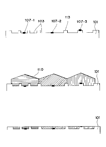
described with reference to Figs. lA to lC.
Substrate
A substrate 101 to be used in the present
invention may be consisted of a material (a stopper
material) which acts as a non-nucleation surface
in crystal forming treatment, and has a slower
mechanical processing speed than that of deposited
crystal to grinding particles in flattening step,
or may be consisted of such material formed on a
subbing substrate. The form of substrate 101 is
not limited, so far as it is proper for crystal
forming treatment and flattening step.
Materials to act as a non-nucleation
surface and also a stopper material, are different
depending on deposited materials. For example,
20S5675
g
1 when a material to be deposited is silicon, glass
such as quartz, etc. or alumina is used, and the
surface of it causes to be a non-nucleation
surface by treatment such as oxidation, nitriding,
etc. Stopper materials include silicon, metals
and so on.
Concavity
In the present invention, monocrystals
finally remain only at the concavity formed on a
substrate. The concavities are formed on a
substrate so as to be fulled with a monocrystal
formed with controlling its position in crystal
forming treatment. The concavities are formed
with the position, number, form and size required
in the following formation of integral circuit,
etc. within the region fulled with a single mono-
crystal. The method for forming the concavities is
not particularly restricted unless it is responsible
for contamination by impurities in the next step.
For example, there is a method comprising forming
a pattern by lithography used in the ordinary
silicon process, followed by etching by wet etching
or reactive ion etching. In the case of forming
concavities on a substrate, the concavities may be
formed on a subbing substrate, followed by forming
non-nucleation surfaces or nucleation surfaces
thereon, or a material having non-nucleation
2055675
-- 10 --
1 surfaces or nucleation surfaces is deposited on
a subbing substrate, followed by forming the
concavities on the upper surface of the material.
Crystal Forming Treatment
A method for forming a monocrystal grain
on a substrate include, for example, the above-
mentioned first and second methods, but are not
limited to these methods.
In the first method, a non-nucleation
surface 103 and nucleation surfaces 107-1, 107-2
and 107-3 are formed on a subbing substrate to
form a substrate (Fig. lA). The nucleation surfaces
may be present on the upper surface of the subbing
substrate or on the surface of a film newly
deposited on the subbing substrate. The nucleation
surface should have a larger nucleation density
for a material constituting a monocrystal than
that of the non-nucleation surface, and also have
a sufficiently small area so as to form only a
single nucleus from which a monocrystal is grown.
The nucleation density of the nucleation surface
may be 102 times, preferably 103 times more than
that of the non-nucleation surface. For example,
in the case that the non-nucleation surface
comprises silicon oxide film or quartz glass,
materials for nucleation surface include silicon
nitride film and silicon oxide, silicon nitride,
11 2055675
1 etc. containing excess of Si, but are not limited
to them.
As shown in Fig. lB, the following step is
a crystal forming step. Methods for forming a
crystal include chemical vapor deposition (CVD)
method, MOCVD method, plasma CVD method, etc.
In the second method a non-nucleation
surface is formed on a subbing substrate, followed
by arranging seed crystals on the non-nucleation
surface instead of nucleation surfaces 107 to form
a substrate. The seed crystals are grown in the
same manner as in the first method to form mono-
crystals.
The non-nucleation surface may be the
surface of the substrate itself or the surface of
a material deposited on the subbing substrate.
The material is not restricted so far as it is an
amorphous insulating material. It is essential in
the present invention that nuclei are not grown
on the non-nucleation surface during crystal
growth. For example, the material for non-nucleation
surface includes a silicon oxide film, quartz
glass, a silicon nitride film and so on.
Prior to crystal forming treatment, minute
monocrystals which are a material constituting -
the crystal, are arranged at the desired positions
as seed crystals. For example, this method
- 12 - 205567~
1 comprises arranging primary seeds having a
sufficiently small surface area so as to aggregate
a material constituting the crystal by heat
treating at the desired positions of the non-
nucleation surface on the non-nucleation surface
with a minute size, and then heat treating the
primary seeds at a lower temperature than the
melting temperature of them under hydrogen
atmosphere to cause them aggregate to monocrystalize
the primary seeds. In addition, seed crystals may
be formed by heat treating a polycrystalline
semiconductor film added with a high concentration
of impurity such as phosphorus, boron, arsenic,
etc. This method is due to monocrystallize-by
abnormal grain growth of a grain in the poly-
crystalline film. The crystal forming treatment
is the same as in the first method. As the result
of the crystal forming treatment, a monocrystal
having the desired size is obtained.
In any crystal forming method, the starting
point for crystal growth may be within the
concavities or outside the concavities (the upper
surface of the substrate).
Flattening Process
After forming crystals on a substrate, -
flattening treatment is carried out. The flattening
is conducted by polishing in this case. For
20S567S
- 13 -
l example, using a polishing apparatus used usually
in polishing of silicon wafers, polishing is
conducted by use of a polishing liquid comprising
a suspension of grinding particles such as colloidal
silica, etc. Crystal grains formed by crystal
forming treatment of the present invention have a
peak form. As progress of polishing, the crystal
grains are polished from their tops parallel to
the surface of the substrate, and polishing is
completed when theupper surfaces of the crystal
grains become the same level as the upper surface
of the substrate which acts as a stopper (Fig. lC).
When a field-effect transistor is formed
in the crystal layer formed thus having a size of
from several ~m to several tens ~m and containing
no crystal grain boundary, for example a single
crystal silicon layer, the transistor exhibits
performances comparable to that of a transistor
formed on a monocrystal silicon wafer.
ZO Constructed complementary field-effect
transistors (C-MOS transistors) are not interferred
with each other because adjacent monocrystal
silicon layers are electrically separated by
silicon oxide. Moreover, because the thickness of
the active layer of device is thinner than that of
2055675
- 14 -
1 Si wafer, erroneous working by charge in the wafer
generated by irradiation of radiation does not
occur. In addition, speed-up of device is possible
because the parasitic capacity of device is reduced.
Monocrystal layers are economically formed on a
substrate having a great area compared with using
Si wafers because any substrate can be used. Also,
because monocrystals can be formed on other
substrates such as semiconductor, piezoelectric
element, dielectric, etc., three dimention integral
circuits with multi-function can be realized.
Examples of the present invention are
described in detail with reference to Figs. lA to
lC and Fig. 4A and Fig. 4B.
Example 1
An example in which a plurality of Si
monocrystal thin films was formed according to the
present invention is described below.
(1) On a fused quartz glass substrate 101
comprising a square having sides of 30 ~m, a
concavity comprising an area of 10 ~m x 26 ~m and
a depth of 10,000 A and two concavities comprising
an area of 10 ~m x 12 ~m and a depth of 10,000 A
were formed by photolithography and etching with a
buffered hydrofluoric acid as shown Fig. 4A.
In this case, the side walls of the
concavities were sloped by side-etching. The
2055675
_ 15 -
1 surface formed thus was a non-nucleation surface
(Fig. lA). For comparison, a substrate having a
surface comprising concavities with the same size
as in the above surface and a depth of 4 ~m formed
by reactive ion etching, was prepared.
(2) Next, a silicon nitride film was
deposited to 1,000 A thickness as a nucleation
surface thin film by reduced CVD method using
dichlorosilane and ammonia. By patterning this
silicon nitride film, as shown in Fig. 4A, silicon
nitride comprising a square having sides of 2 ~m
was arranged as a nucleation surface 107 at the
stopper position between the above three concavities
(Fig. lA).
(3) When these substrates were set on a
CVD apparatus, by crystal forming treatment under
the conditions of 80 Torr, 1050 ~C and SiH2C12/HCl/H2
= 0.53/1.5/100 (l/min), Si nucleus was formed only
on the silicon nitride area. As continuing
crystal growing, the crystal was isotropically
grown from the nucleation surface, contacted with
the adjacent crystal, and further fulled the
void of the concavity to form a square having
sides of 30 ~m of which shape was a peak shape
having a height of 20 ~m (Fig. lB).
(4) Then, monocrystals were polished
using a processing luquid containing colloidal
2055675
- 16 -
1 silica (an average particle size: 0.1 ~m) comprising
silicon oxide by use of an ordinary silicon wafer
surface-polishing apparatus under a pressure of
100 g/cm at 30 ~C to 40 ~C. As the result, as
shown in Fig. lC, Si monocrystals were polished,
and polishing was completed when Si monocrystals
became the same level as the stopper 113 to give
a flat Si monocrystal thin film having a thickness
of 10,000 A + 400 A on the 4 inch fused quartz
glass substrate.
In other 9 sheets of substrate simultaneously
polished, the obtained Si monocrystal thin films
had a thickness of 10,000 A + 500 A. When the
cross-section of the monocrystals were observed by
defect actuarizing etching, that is, secco etching,
defect was not found particularly near the side
walls, and void was not generated, and the
crystals had good crystallinity. On the other
hand, for comparison, when the cross-section of
monocrystals formed on the comparative substrate
containing concavities having a depth of 4 ~m
were observed similarly by secco etching, a void
had been formed under the lower part of the side
wall of concavity, and defect had been formed on
the upper part of the level-difference, which is
assumed to be introduced when the crystal get over
the level-difference.
205S675
_ 17 -
1 (5) A NAND circuit was formed on these
monocrystals using MOS transistors prepared by
use of ordinary semiconductor process as shown in
Fig. 4B. In Fig. 4B, two n-MOS transistors were
formed on the concavity 401, and p-MOS transistor
was formed in the concavities 402 and 402',
respectively. 403, 404, and 405 are a p-type
semiconductor region comprising source and drain
of n-MOS transistor. 406, 407, 408 and 409 are
an n-type semiconductor region comprising source
and drain of p-MOS transistor. The above regions
were formed by ion implanting As and B into
monocrystals in the concavities, respectively. 410
and 411 are gate electrodes formed on the gate
oxide film. A gate length L and a gate width W
were L/W = 6 ~m/10 ~m in n-MOS and L/W = 3 ~m/10
~m in p-MOS, respectively. Therefore, although
the concavities were different in size and form,
no crystal grain boundary was present in the
concavities because the crystals were grown with
fulfilling all the three concavities, and per-
formances of the transistors were comparable to
that of transistors formed monocrystal silicon
wafers.
Example 2
Example 2 in which a plurality of Si
monocrystal grains was formed according to the
205S67~
- 18 -
1 present invention is described below.
(1) On an Si wafer substrate, a silicon
oxide film was deposited to 13,000 A thickness by
heat oxidation method, and then rectangular
concavities having an area of 8 ~m x 28 ~m and a
depth of 5,000 A were formed at 2 ~m intervals by
photolithography and etching with a buffered
hydrofluoric acid. The surface formed thus was a
non-nucleation surface (Fig. lA).
(2) Next a silicon nitride film was
deposited to 300 A thickness on the substrate by
LPCVD method. Then, by patterning this silicon
nitride film by photolithography used in the
ordinary semiconductor process and reactive ion
etching (RIE), squares of SiN4 having sides of 2
~m were arranged as nucleation surfaces 107 in
lattice pattern at 30 ~m intervals, where the
nucleation surface was placed at the each center
of the concavities (Fig. lA).
(3) On the above substrate, crystal
forming treatment was carried out by CVD method
using dichlorosilane, hydrogen chloride and
hydrogen. The conditions for crystal growth were
as follows. SiH2C12/HCl/H2 = 0.53/1.4/100 (l/min),
990 ~C, 80 Torr. As the result, a crystal was
isotropically grown from the nucleation surface,
contacted with the adjacent crystal, and further
2055675
-- 19 --
1 fulfilled the void of the concavity to form a
square having sides of 30 ~m, where the crystal
shape was a peak form having a height of about 20
~m.
(4) Then, Si monocrystals were polished
using a processing liquid containing colloidal
silica (an average particle size: 0.1 ~m) of SiO2
by an ordinary silicon wafer surface-polishing
apparatus under a pressure of 100 g/cm2 at 30 ~C
to 40 ~C. As the result, as shown in Fig. lC, Si
monocrystals were polished, and polishing was
completed when Si monocrystals became the same
level as the stopper 113 which was the silicon
oxide film region directly formed on the substrate
to give a flat si monocrystal thin film having a
thickness of 5,000 A + 200 A in each concavity on
the 4 inch Si wafer substrate. In other 9
sheets of substrate simultaneously polished, the
obtained Si monocrystal thin films had a thickness
O O
of 5,000 A + 250 A.
Example 3
(1) On a fused quartz glass substrate 101,
rectangular concavities having an area of 5 ~m x
15 ~m and a depth of 5,000 A were formed at 5 ~m
intervals by photolithography and reactive ion
etching. The surface formed thus was a non-
nucleation surface (Fig. lA).
2055675
- 20 -
l (2) Next, a polycrystalline silicon film
was deposited to 2,000 A thickness on the surface
by LPCVD, and then P (phosphorus) was implanted
as an impurity into the silicon film at an
acceleration voltage of 30 KeV and 2 x 10 5cm
Then, by patterning the silicon film by photo-
lithography used in the ordinary semiconductor
process and reactive ion etching (RIE), squares
of polycrystalline silicon film having sides of
1.2 ~m were arranged as primary seeds at 20 ~m
intervals in lattice pattern, where the each
primary seed was placed at the stopper region
between the adjacent concavities (Fig. lA).
(3) Next, the substrate was heat treated
at 1,100 ~C under hydrogen atmosphere for 3 min.
As the result, each primary seed was aggregated
to form a monocrystal seed.
(4) On the above substrate, crystal
forming treatment was carried out by CVD method
using dichlorosilane, hydrogen chloride and
hydrogen. The conditions for crystal growth were
as follows. SiH2C12/HCl/H2 = 0.53/1.6/100 (l/min),
1,040 ~C, 80 Torr. As the result, a monocrystal
having a particle size of 28 ~m was formed from
each nucleation surface as the starting point.
(5) Then, Si monocrystals were polished
using a processing liquid containing colloidal
2055675
- 21 -
1 silica (an average particle size: 0.1 ~m) of SiO2
by an ordinary silicon wafer surface-polishing
apparatus under 100 g/cm at 30 ~C to 40 ~C. As
the result, as shown in Fig. lC, Si monocrystals
were polished, and polishing was completed when
Si monocrystals became the same level as the
stopper 113 to give a Si monocrystal thin film
having a thickness of 5,000 A + 200 A each on the
4 inch fused quartz glass substrate. In other 9
sheets of substrate simultaneously polished, the
obtained Si monocrystal thin films had a thickness
f 5 000 ~ + 250 A
Example 4
(1~ On a Si wafer substrate, a silicon
oxide film was deposited to 10,000 A thickness by
heat oxidation method, and then rectangular
concavities having an area of 5 ~m x 15 ~m ar.d
a depth of 8,000 A were formed on the substrate
at 5 ~m intervals by photolithography and etching
with a buffered hydrofluoric acid. Then, a
silicon nitride film was formed to 1,000 A
thickness on the concavities by LPCVD method.
The surface formed thus was a non-nucleation
surface (Fig. lA).
(2) Next, a polycrystalline silicon film
doped with P (phosphorus) of 3 x 10 5 cm 2 was
deposited to 250 A thickness on the surface by
205S675
- 22 -
1 LPCVD method. By patterning this silicon film by
EB (electron beam) exposure method, squares of
polycrystalline silicon film having sides of 0.3 ~m
were arranged as primary seed at 20 ~m intervals,
where each primary seéd was placed at the stopper
region between the adjacent concavities (Fig. lA).
Next, the substrate was heat treated at 990 ~C
under hydrogen atmosphere for 2 min. to convert
the primary seeds to monocrystal seeds.
10(3) On the above substrate, crystal
forming treatment was carried out by CVD method
using dichlorosilane, hydrogen chloride and
hydrogen. The conditions for crystal growth were
as follows. SiH2C12/HCl/H2 = 0.53/2.0/100 (l/min.),
15990 ~C, 80 Torr. As the result, a monocrystal
having a particle size of 28 ~m was formed from
each nucleation surface as the starting point.
(4) Then, Si monocrystals were polished
using a processing liquid containing colloidal
silica (an average particle size: 0.01 ~m) of
SiO2 by an ordinary silicon wafer surface-polishing
apparatus under a pressure of 100 g/cm2 at 30 ~C
to 40 ~C. As the result, as shown in Fig. lC, Si
monocrystals were polished, and polishing was
completed when Si monocrystals became the same
level as the stopper 113 which was the silicon
oxide film region directly formed on the substrate
- 23 _ 2055675
1 to give a flat Si monocrystal thin film having a
thickness of 8,000 A + 400 A in each concavity on
the 4 inch Si wafer substrate. In other 9 sheets
of substrate simultaneously polished, the obtained
Si monocrystal thin films had a thickness of 8,000
O O
A + 450 A.
As described above, according to the method
for forming crystal articles of the present
invention, monocrystal thin films can be formed
on an amorphous substrate in the state that each
monocrystal thin film is surrounded by an
insulator region and is flat and precisely
controlled at the desired positions with the
desired form. Accordingly, integral circuits can
be formed without lengthening wiring and also with
small limitation in device arrangements. Integral
circuits utilizing characteristics of monocrystal
thin film can be formed without variation of the
performances and also with a higher integral
degree and yield.