Note: Descriptions are shown in the official language in which they were submitted.
TITLE OF THE INVENTION
IMAGE PICK UP DEVICE
FIELD OF THE INVENTION
This invention relates to an image pick up device
having a plurality of rows of light receiving cells
for converting an optical image into an electrical
signal.
PRIOR ART
Conventional video cameras produce pictures having
a narrower dynamic range than conventional silver
halide photograpic film. In such cameras there is,
therefore a tendency for extremely bright parts and
extremely dark parts of an image to become plain white
and plain black respectively. In conventional video
cameras, a known technique for compensating for this
phenomenon is to adjust the iris.
However, defects may still ~ in, such that not all
of the image can be adjusted to a proper level because
of the limited d~namic range.
.s
; , , . . . . ,~ . , "
. : ~, . . i . ~ ,
:, , ., ~ :
2~5~867
This problem can be solved by for example synthesising
two images, one of which has an exposure period of 1/60
second while the other has an exposure period of
1/1000 second. In this method the two images have an
exposure period which differs by a factor of sixteen,
so that the dynamic range can be expanded by about 16
times, making it as wide as that for photography. This
technique is disclosed in, for example, Japanese Laid
Open Patent 1-176173, and Japanese Laid Open Patent
63-306779 etc.
JP 1-176173 has an interline transfer typé CCD which
has many pairs of vertical transfer CCD elements,
located adjacent to both sides of each vertical row of
light receiving cells. Each vertical transfer CCD
stores the respective image signal which was formed by
a predetermined exposure of a different period from
the period of another image signal. However,
according to the disclosure, each vertical row of -
light receiving cells has two vertical tranfer CCD~s,so that each light receiving cell can only have a
small, limited, light receiving area and therefore has
low sensitivity.
2055~67
JP 63-306~79 uses an ordinary image pick up device,
it changes the exposure period field by field and it
synthesises two consecutive fields, so that the
synthesised image has insufficient definition if an
object is moving.
SUMMARY OF THE PRESENT INVENTION
An object of the present invention is to provide an
improved image pick up device. Another object is to
provide an improved video camera.
According to an aspect of the present invention, there
is provided an image pick-up device comprising: a
plurality of rows of light receiving cells for
converting an optical image into an electrical signal;
a plurality of transfer registers each located
adjacent to a corresponding row of light receiving
cells, said registers being arranged to receive a
charge signal from said row of light receiving cells
and to transfer said charge signal serially to read it
out, wherein said transfer registers are light
shielded; and a control circuit for driving said light
receiving cells and the t~:ansfer regis-ters;
characterised in that: the control circuit clears
' ' ' ' ' . ,' , '
'
2 ~ 6 ~
unnecessary charge in said light receiving cells,
transfers charge signals generated in the light
receiving cells to the transfer registers after a
first exposure period and carrys out a second exposure
for a second exposure period that is different from
said first exposure period for storing a first and a
second image signal in the pick-up device.
The invention provides the advantage of increasing
dynamic range without reducing the effective light
receiving area. Furthermore, in one field period, two
consecutive images can be obtained, ensuring that a
synthesised image will not lose resolution even if an
object is moving.
Further features, aspects, objects and advantages of
the present invention will be apparent from the
following description of an embodiment given by way of
non limiting Example.
BRIEF DESCRIPTION OF THE DRAWINGS
Fig. 1 illustrates a plan view of an image pick up
devi~e of a first embodiment;
,
2~5~7
Fig. 2 illustrates a timing chart of the first
embodiment;
Fig. 3 illustrates a plan view of a second embodiment
of the present invention;
Fig. 4 illustrates a schematic circuit diagram of the
present invention;
Fig. 5 illustrates a timing chart of sampling pulses
used in the circuit shown in Fig. 4;
i.
Fig. 6 illustrates the relationship between amount of
light and signal level;
Fig. 7 illustrates a schematic circuit diagram of a
third embodiment;
Fig. 8 illustrates another type of image pick up -
device applicable to the third embodiment of the
present lnvention;
2 ~ 7
-- 6
Fig. 9 illustrates a sectional view of the image pick
up device shown in Fig. 8;
Fig. 10 illustrates a timing chart of the third
embodiment of the present invention;
Eig. 11 illustrates another part of the timing chart
of the third embodiment;
Fig. 12 illustrates a schematic circuit diagram of the
third embodiment.
DETAILED DESCRIPTION OF THE ILLUSTRATIVE EMBODIMENT
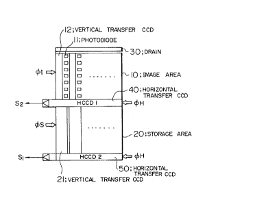
In Fig. 1, numeral 10 denotes an image area, 20
denotes a storage area, 30 denotes a drain, 40 and 50
denote horizontal transfer charge coupled devices,
CCD's.
The image area 10 consists of photodiodes 11 and a
plurality of vertical transfer CCD's 12 for storing
charge signals generated in said photodiodes 11, after
a photoconversion operation. The vertical row of
photodiodes 11 and the vertical transfer CCD's are
arranged vertical row by ve~ltical row. The vertical
transfer CCD's 12 are light shielded, and the stored
. . .
20~67
charge signal is transferred to the storage area 20 by
a vertical transfer pulse ~I.
The drain 30 is located at the upper end of the image
area 10 for removing unnecessary charges generated in
said image area 10.
.
The storage area 20 is also light shielded and
consists of a plurality of vertical transfer CCD's 21
for storing vertically transferred charges from the
image area 10. The horizontal transfer CCD 40 is
located between the image area 10 and the storage area
20, while the horizontal transfer CCD 50 is located
below the storage area 20. The horizontal transfer CCD
40 and the horizontal transfer CCD 50 transfer charge
signals respectively via said vertical transfer CCD 12,
21 to an output amplifier.
An operation of the above mentioned image pick up
device will be explained with reference to Fig. 2.
The photodiodes 11 are exposed twice within one field
period; Tl denotes a first exposure period and T2
denotes a second exposure period. Tl is loDger than
T2.
~ . ,
.
CA 020~867 1998-02-11
At the end of the first exposure period T1, reverse
transfer pulses ~I, identified as A in the Figure, are
supplied to the vertical transfer CCD 12 in order to
transfer unnecessary charge remaining in the vertical
transfer CCD 12 to the drain 30. Thereafter, a transfer
pulse ~I, identified as B in the Figure, is supplied to
the vertical transfer CCD 12 for transferring charges
generated in the photodiodes 11 to the vertical transfer
CCD 12. Transfer pulses ~I, identifies C, and transfer
pulses ~S, that is dubbed C', are supplied to the image
pick up device to transfer charge from said vertical
transfer CCD 12 to- the storage area 20, while the
photodiodes 11 are under the second exposure period T2
after the pulse B.
Next, transfer pulses ~I, identifies as D, are supplied
to the image pick up device to transfer charge generated
in the second exposure period T2 to the vertical transfer
CCD 12.
At this phase in the vertical transfer CCD 21, charge
signals generated in the first exposure period T1 are
stored, while charge signals generated in the second
20~8~7
g
exposure period are stored in the vertical transfer
CCD 12.
After the completion of a vertical blanking period, a
transfer pulse ~I, (referred to as E) and transfer
pulse ~S, (referred to as E'), are supplied to the
image pick up device for each horizontal blanking
period of each horizontal period Tn, in the video
image period. Therefore, the charge signal in the
vertical transfer CCD 12 and the charge signal in the
vertical transfer CCD 21 are transferred,
respectively, to the horizontal transfer CCD 40 and to
the horizontal transfer CCD 50.
The charges are amplified by output amplifiers during
the video scanning period of each horizontal period,
in response to the horizontal transfer pulse ~H. Here,
an output signal from the horizontal transfer CCD 40
is identified as S2 and an output signal from the
horizontal transfer CCD 50 is identified as Sl.
Fig. 3 illustrates a plan view of the second
embodiment of the present invention, in which similar
components, or corresponding components in different
fields, are denoted by the same reference numerals.
., ~ .
.. . . . : , ~. ~ ~ , ... .
... . -
.
- . , .. , . .
fi 7
-- 10 --
In this embodiment, the horizontal transfer CCD 40 is
omitted and the first image and the second image are
stored, in the storage area 20 and the ver-tical
transfer CCD 12 respectively, in the same way as the
first embodiment before the reading out operation.
~owever, the two images are read out through the
horizontal transfer CCD 50 sequentially.
The read out charge signal generated by the first
exposure is stored in a memory 60, and read out at the
same time as the signal S2 generated by the second
exposure, which is read out fr~m the horizontal
transfer CCD 50.
In the first and the second embodiments of the present
invention, signals Sl and 52 are obtained at the same
time, therefore a subsequent processing circuit for
synthesising signals can be simplified. Compared to
the prior art, such as Japanese Laid Open Patent
1-176173, this invention has higher sensitivity
because it does not limit the effective light
receiving area, and the first and second exposure
operations are carried out continuously so that a
higher resolution can be obtained compared to the
2 ~ 7
11 --
prior art, such as Japanese Laid Open Patent 63-306779
even if an object is moving.
A video camera that is suitable for the image pick up
devices described will be explained with reference to
Figs. 4, 5 and 6, in which, Fig. 4 illustrates a
schematic circuit diagram of the video camera, Fig. 5
illustrates a timing chart of sample hold pulses for
synthesising signals Sl, S2, and Fig. 6 illustrates
the relationship between amount of light and signal
levels in the video camera.
The video camera has an optical system 100, a camera
signal processing system 200 and a recording system
300, as shown in Fig. 4. In the optical system 100, an
amount of light which passes through a lens 101 is
restricted by an iris 102, before being focussed on a
sensor 103. The sensor 103 is driven by a sensor
driving circuit 105 and the iris 102 is driven by an -
iris driving circuit 106. '
The signals Sl, S2 are processed in the camera signal
processing system 200 so as to expand dynamic range.
,.,
2~g67
- 12 -
The signal Sl, that is signal a, from the sensor 103
is saturated at the level vsat (Fig. 6) when a large
amount of light is incident on the sensor 103. The
signal Sl, that is an output signal a, is clamped to
the level of its black portion, by a clamp circuit
221, wherein vc denotes a clamp voltage.
A signal portion that extends beyond a signal level
Vthl + Vc of the signal Sl that is clamped to the
voltage Vc, that denotes a', is clipped by a white
clip circuit 222, so that a curve a'' is folded, as
shown in Fig. 6. The white clip operation is performed
to eliminate noise generated by the sensor. The noise
level increases, particularly around the saturation
level of the sensor.
A level detector 223 is connected to an output
terminal of the sensor 103 for the signal Sl, for
detecting whether the signal level is saturated or
not. In this embodiment, the detecting threshold
level is set at the same level as the white clip level
Vthl.
: ~ . .,, . . . : ..
5~7
- 13 -
A level detector 223 is connected to a control circuit
225 for making the control circuit 225 produce sample
and hold pulses SHl, SH2, which are for controlling
sample and hold switches 216 and 226 respectively, the
pulses being shown in Fig. 5. The control circuit
225 controls an iris driving circuit 106 so as to
adjust the iris 102 properly, according to a
statistical level distribution of the signal Sl which
is detected by the level detectors 223, 224. Here,
the detection level of the level detector 223 is Vthl,
and the detection level of the level detector 224 is
Vth2.
The signal processing method for the signal S2 from
the sensor 103 will now be explained. While the signal
level of the signal S2 is about l/16th of the level of
the signal Sl, and the gain of amplifier 213 is set at
unity, the signal S2 that corresponds to an output
signal b is supplied to a clamp circuit 214 through
the amplifier 213 as a signal b.
Signal Sl (shown as a curve a in Fig. 6) is input to
the level detector 223 and, if the level of the signal
~- Sl is over the level Vthl, it is detected by the level
detector 223 and the signal Sl is clamped and clipped
5~
- 14 ~
by the white clip circuit 222, (shown as a curve a"
in Fig. 6). Therefore, a signal that is over the
level Vthl + vc of the signal Sl should be replaced by
the signal S2.
The signal level of signal S2 (an output s.ignal b)
corresponding to the signal level Vthl of the signal
Sl (an output signal a) is identified as VLSl and the
level of VLSl is defined as follows:
VLSl = Vthl x T2/Tl ~ Vthl/16
~ere, a signal portion of the signal S2 (shown as a
straight line b in Fig. 6) which is over the level
VLSl should be added to a signal portion of the signal
Sl (shown as a curve a~' in Fig. 6) which is over the
signal level Vthl + VC. Then, the clamp voltage VC'
of the clamp circuit 214 should be set at the voltage
which is Vthl - VLSl higher than that clamp voltage VC
of the clamp circuit 221.
The signal passed through the clamp circuit 214 is
supplied to the .input of a sample and hold swi-tch-216,
which is actuated by a sample and hold pulse SHl from
the control circuit 225, when signal Sl is saturated.
2~8~7
- 15 -
Therefore, signal Sl (that is an output signal of the
white clip circuit 222, and shown as a curve a' in
Fig. 6) is sampled and held in a hold condenser CH
when the signal Sl is not saturated, and the signal S2
(an output signal of the clamp circuit 214) is sampled
and held when the signal Sl is saturated. In this way
the signals Sl and S2 are synthesised as shown by
curve c in Fig. 6. A high level portion of this
synthesised signal is then suppressed by a knee
circuit 231.
In this embodiment, the knee circuit 231 suppresses
the high level signal portion by making it 1/4 of the
input signal. The knee processed signal d is further
processed in a camera process circuit 232, providing
gamma compensation, etc.
An output of the camera process circuit 232 is
introduced to the recording device 301, such as video
tape or floppy disk.
If the incident light applied to sensor 103 is not
particularly strong, the dynamic range does not have
to be as w ~e as in the previous example. An example
- 16 -
will now be described in which the dynamic range may
be increased by a factor of eight.
A level detector 210 detects the statistical frequency
at which a signal level is over the level Vthl (nearly
equal Vthl/1~6), while the level detector 211 detects
the statistical frequency of the signal level which is
over the level Vth2' (nearly equal Vth2/1/6~.
If the detected frequency of the level detector 210 is
high, the control circuit 212 makes the exposure
period T2 short, that is shorter than 1/1000 second.
If the detected frequency of the levèl detector 210 is
low, because the brightness of the image is not so
high, the controI circuit 212 doubles the gain of the
amplifier 213.
The two times amplified signal v' is supplied to the
clamp circuit 214 and the clamp voltage VC' is defined
by the following equation.
VC' = VC -~ Vthl - Vthl/8
-, . , .. ~. . .- :. . :
- 17 -
Thus as an output of the clamp circuit 214 becomes
signal c~, this signal c~ is converted -to a signal d~
by the knee circuit 231. Therefore, according to the
strength of the incidental light, the characteristic
of an output from the knee circuit 231 is optimised
and an input signal level to a camera process circuit
232 is also optimised.
Fig. 7 illustrates a partial circuit block diagram of
another embodiment of the video camera, in which the
input si~nal level adjustment for the camera process
circuit 232 is carried out by the knee circuit 231
instead of by the amplifier 213.
The control circuit 212 controls a knee characteristic
of the knee circuit 231 according to the output of the
level detector 210 and 211, that is according to the
statistical freguency of the signal level, so as to
adjust the slope of a knee curb in Fig. 7 to for
example 1~4, or 1/2 etc.
The long exposed light signal and the short exposed
light signal can be read out simultaneously,
deterioration of the ~esolution or the sensitivity can
be prevented and a wide dynamic range can be obtained.
,..... ;, . .
- . ,
. .
' 2~86~
- 18 -
Furthermore, because of the aforementioned
simultaneous reading out, the following camera signal
processing circuit can be simplified.
A further embodiment of the present invention will be
explained, with reference to Fig 8, which illustrates
an image pick up device and with reference to Fig. 9,
which illustrates a sectional view of the image pick
up device of Fig. 8.
In Fig. 8 numeral 430a denotes an image area
consisting of rows of photodiodes 430c and vertical
transfer CCDs 430b, for storing charge signals
generated in the photodiodes 430c after a
photoconversion operation. The rows of photodiodes
430c and the vertical transfer CCD's 430b are
alternately arranged in the image area 430a.
Each vertical transfer CCD 430b is light shielded, and
transferred charge signals from the photodiodes 430c
are further transferred to a horizontal tranfer CCD
430d by each vertical transfer pulse ~I which is
supplied in each hori~ontal blanking period of each
hori~ontal period. The vertical transfer CCD 430b and
20~67
-- 19 --
the horizontal transfer CCD 430d constitute the
transfer means.
In this embodiment, the pick up device is not limited
to the one which is shown in Figs. 8 and 9, for
example the image pick up devices such as shown in
Figs. 1 or 3 may be applied to this embodiment.
The charge signal stored in the horizontal transfer
CCD 430d is transferred to the output amp 430e by
horizontal transfer pulses ~H and is then converted to
a voltage signal for the output.
Unnecessary charge stored in the photodiodes 430c are
eliminated to the CCD substrate (that is N type
semiconductor substrate 401 in Fig. 9) by supplying
said pulses ~SH.
As shown in Fig. 9, a first well 402 over a P type
semiconductor is formed on the N type semiconductor
substrate 401, and an N type semiconductor region 403
is formed in the first well 402 for constituting a
photodiode 430c. A a second well 404 of P type
semiconductor and N type semicond~ tor area 405 are
formed in t:he first well 402 for constituting the
2 ~
- 20 -
vertical transfer CCD 430b. Polycrystal region 406 is
formed as a transfer gate above the first well 402 of
P type, which is between the N type semiconductor
region 403 and the N type semiconductor
region 405, above the N type semiconductor region
5. Above the polycrystal region 6, an Al layer 407 is
located for light shielding. Between sensor regions,
consisting of a photodiode 430c and a vertical
transfer CCD 430b, a channel stop region is formed by
P type semiconductor regions 408.
Here the N type semiconductor region 403 and the N
type semiconductor region 405 respectively correspond
to a drain region and a source region of a N channel
lS insulated gate type transistor. Charge accumulated
in the N type semiconductor region 403 is transferred
to the N type semiconductor region 405 when a positive
voltage ~I is applied to the polycrystal region 406 of
the gate. sy applying a negative voltage ~I to the
polycrystal region 406, a vertical transfer operation
by the vertical transfer CCD 430b is carried out.
Meanwhile, in Fig. 8 and ~ig. 9, Xa denotes a draining
.~'? channel for unnecessary charge in the photodiode 430c.
Xb denotes a transfer channel of photocharge from the
. : : ,.:, ,:.:: , . . ~ :
- 21 -
photodiode 430c to the vertical transfer CCD 430b. Xc
denotes a -transfer channel for signal charge from the
vertical transfer CCD 430b to the horizontal transfer
CCD 430d. Xd denotes a transfer channel for signal
charge in the horizontal transfer CCD 430d.
Operation of this embodiment will be explained with
reference to Fig. 10, which illustrates a timing
chart.
TSl denotes a period for a first exposure of a short
period exposure operation and TS2 denotes a period of
a second exposure at a long period exposure
operation.
TS1' denotes a period for transferring a signal
generated during the first exposure and TS2' denotes a
period for transferrring a signal genera-ted during the
second exposure.
One of the features of this embodiment is that the
first exposure and the second exposure are carried out
substantially continuously.
. .
.. ... . ..
~: .
2~5~67
-- 22 --
As shown in Fig. 10, by applying a shutter pulse ~SH
~Pa in Fig. 10) to the CCD substrate (N type
semiconductor substrate ~01), charges in the
photodiodes 430c are drained, thereby allowing a
photoconversion operation to be initiated.
Next, by applying a pulse ~I (Pb in Fig. 10),
photocharge in the photodiode 430c is transferred to
the vertical transfer CCD 430b and the first exposure
period is terminated. In this embodiment, this
operation is called a CCD shutter operation.
The second exposure operation will now be explained.
After the first exposure operation, the photodiode
lS 430c subsequently starts the second exposure operation
as the long period exposure operation. This second
exposure operation can be finished after the
photocharge generated in the first exposure operation
has been completely transferred to the vertical
transfer CCD 430b. During this period, the photocharge
generated by the first exposure is read out from the
image sensor; the period TSl' being within the period
TS2. The signal charge in the vertical transfer CCD
430b is tr~asferred to the horizontal transfer CCD
430d by the pulse ~I (Pc in Fig. 10) in each
- . ., . :, : : . . . .
2 ~ S '~
- 23 -
horizontal blanking period, and is output from the
image sensor through the output amplifier 430e by
supplying the pulse ~H (Pd in Fig. 10) in the
horizontal ef~ective period.
After the transferring operation of the signal
generated in the first exposure operation, by
supplying pulse ~2 (Pb' in Fig. 10), the photocharge
generated in the second exposure operation is
transferred to the vertical transfer CCD 430b from the
photodiode 430c, thereby finishing the second exposure
operation.
After the second exposure operation, the photocharge
generated during the second exposure operation is
output from the image sensor in the same way as the
signal generated by the first exposure operation, by
supplying the pulses ~2 (Pc' in Fig. 10) and the
pulses oH (Pd' in Fig. 10).
Thus, in accordance with this embodiment, by using
only a general purpose low cost CCD, the short period
exposure operation and the long period exposure
operation can be performed with minimal time lag.
'..'.~, ' . ~ . - ' --
- ~., . :
2~8~7
- 24 -
Furthermore, by synthesising both signals, an expanded
dynamic range can be obtained.
Fig. 4 illustrates a timing chart of a fourth
embodiment of the present invention, in which the
difference from the third embodiment, shown in Fig.
10, is that the ending of the second exposure
operation is controlled by a shutter member.
The shutter comprises a mechanical shutter, or an
optical shutter, that is consisting of a material such as
a liquid crystal. The shutter is normally open and
while open, the first exposure operation is carried
out in the same way as the aforementioned CCD shutter
operation. In the third embodiment, shown in Fig.
10, the second exposure period TS2 should be longer
than the transferring period TSl' for the signal
generated during the first exposure period, because
the signal generated during the second exposure period -
cannot be transferred to the vertical transfer CCD
until the transferring operation of the signal
generated during the first exposure period is
finished. On the contrary to the third embodiment, in
this embodiment, by adopti~ another shutter member,
the second exposure period can be terminated before
2 ~
the completion of the transferring opera-tion of the
signal generated in the first exposure period.
The abovementioned embodiments may be applied not only
to a movie video camera, but also to a still video
camera. For example, in the third embodiment, the
signal generated by the short exposure operation and
the signal generated by the long exposure operation
can be obtained alternately field-by-field, so these
signals can be processed as an ordinary movie video
signal, in a movie video camera. Furthermore, by
selecting one of the signals, it can be recorded in a
still video camera system.
In the fourth embodiment, shown in Fig. 11, if the
shutter member is such as a rotary shutter member,
the signal generated by the short period exposure
operation and the signal generated by the long period
exposure operation can be obtained field-by-field so
as to be suitable for the movie video camera.
Furthermore, if the shutter member is formed by an
i-is shutter, a liquid crystal shutter or a focal
plane shutter, one of the field signals cor~esponds
to the signal generated by the short exposure
operation and the signal generated by the long
:,, ., . ,. :.,., ~ . :
- . . . .. ~., , . , ,, - ,
CA 020~867 1998-02-11
- 26 -
exposure operation can be selected for the still video
camera.
In the fourth embodiment shown in Fig. 11, the long
exposure operation can be carried out in advance of the
short exposure operation. In this case, more precise
exposure operations can be carried out because the CCD
shutter operation is more precise than the mechanical
shutter member and the signal generated by the long
exposure operation is more important than the signal
generated by the short exposure operation in the
synthesised signal.
Fig. 12 illustrates a schematic circuit diagram of
another embodiment of the video camera.
In the figure, an optical image is focussed on the
sensor 430 through a lens 410 and an iris 420. The
sensor 430 is driven by a sensor driver circuit 440
controlled by a control circuit 470. The iris 420 is
controlled by an exposure member driver circuit 450
which is controlled by the control circuit 470 based
on a signal output from the sensor 430. Here, if the
video camera shown in Fig. 12 is a still video camera,
~5~6~
- 27 -
as mentioned before, the iris is closed after the
second exposure operation.
A camera signal processing circuit 460 carries out
conventional knee suppression or gamma conversion
processing. Circuit 460 also performs analog to
digital conversion by an A to D converter 480, so
that, in this embodiment, the signal generated by the
first exposure operation is converted into a digital
signal and is then stored in a memory 490.
In an operational circuit 100, the synthesising
operation is carried out by combining the signal
generated by the first exposure operation, read out
from the memory 490, and the signal generated by the
second exposure operation output from the A to D
converter 480, for expanding the dynamic range. A
control signal for this synthesising operation is
generated by the control circuit 470 and, by detecting
the saturation of the signal generated by the second
exposure operation (the long exposure operation), the
detected saturated signal is replaced by the signal
generated by the first exposure operation, that is the
short exposure operation.
.
- , "
- . : .. , . :
- : . ..
2 ~ 7
- 28 --
The synthesised signal from the operation circuit 100
is converted to an analogue signal by a D -to A
converter 110 and is then introduced to a recording
system.
As explained above, by this fourth embodiment, -the
second exposure operation can be controlled by another
shutter member, such as the mechanical or electronic
shutter, so that the period of the second exposure can
be set freely to some extent. Therefore, even a high
speed moving object can be picked up with expanded
dynamic range and high resolution.