Note: Descriptions are shown in the official language in which they were submitted.
: The present invention relates to a method of preparing a
printed substrate. More particularly, it relates to a method
of preparing a printed substrate in which solder is coated on
a wiring pattern.
Aspec~s of the prior art and present invention will be
described by reference to the accompanying drawings in which:
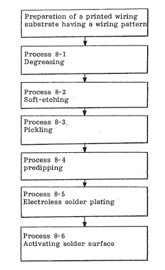
Figure 1 is a flow chart showing the processes o~
electroless plating as major processes in detail in a
method of preparing a printed substrate according to
Example 1 of the present invention;
Figure 2 is a diagram in cross-section which shows a
surface portion of the printed substrate prepared by the
electroless plating in Example l;
Figure 3A is a picture showing the surface area of a
æolder layer formed on the printed substrate;
Figure 3B is a picture which shows a part of the
solder l~yer in a large scale;
Figure 4 is a characteristic diagram showing
xelations of the thickness of the solder layer and the
formulation of tin in the layer shown in Figure 3;
Figure 5 is a characteristic diagram showing the
relation of plating time and the thickness of the solder
layer in an electroless plating process in Figure l;
~aL I `
.
,
Figure 6 shows an example obtained by soldering an IC ::
package on the solder layer in Figure 3 wherein Figure 6A
is a picture showing a state at a soldered portion and
Figure 6B is a picture showing a part of the soldered
portion in a large scale;
Figure 7 is a diagram illustrating how solder is
coated on a printed substrate by means of hot-air-
leveling method;
~ igure 8 is a diagram in cross-section showing a
surface area of a printed substrate prepared by a
conventional method; and
Figure 9 is a diagram in cross-section showing
another example of a surface area of a printed substrate
prepared by a conventional method.
A conventional method of coating solder on a wiring
pattern of copper on a substrate w.i'il be described, by
taking a hot-air-levelin~ method as an e~ample, with
reference to Fi~ure 7.
The printed substrate 1 which has been subjected to a
patterning operation and the coatiny operation of a
solder resist is im~ersed for a predetermined time in a
vessel 2 in wbich the solder 3 is received in a molten
state. When the printed substrate ~ is raised from the ~:
vessel, gas 4 of high temperature and high pressure is
blasted on the su~strate surface to blow off an excessive
amount of solder deposited on the wiring pattern of
copper; thus the solder is covered at a predetermined
- la -
'
- , .
:
a6~8
- 2 -
portion of the wiring pattern of copper.
A method of preparing a multi-layered printed
' substrate in which the above-mentioned solder coating
technique is used will be described.
; 5 Process 1: patterning electric conductive plates
; which constitute inner layers.
Process 2: treating the surface of the electric
conductive plates constituting inner layers ~blackening).
; Process 3: laminating layers including the inner
layers and pressing the lamination.
Process 4: forming a through hole in the lamination.
Process 5: copper-plating the lamination.
Process 6: patterning wire lines on the lamination.
Process 7: printing a solder resist and symbols.
Process 8: hot-air-leveling of solder.
Process 9: processing the outer configuration of the
printed substrate.
However, the conventional method of preparing a
printed substrate had problems as follows. Namely, as
shown in Figures 8 and 9, it was difficult to uniformly
and evenly cover the solder 6 on the copper wiring
pattern 5, and the thickness of the solder layer was apt
to be large due to the interfacial tension of the solder
6 at the portion where the surface area of the copper
wiring pattern was small and the distance between the
patterned wires was narrow, whereby there was a danger of
short-circuitting between adjacent wires (as indicated by
2~362:~&
A in Figure 8). On the other hand, when a pressure of
gas 4 for blowing off an excessive amount of the solder 6
was made large in order to avoid the danger of short-
circuitting, the thickness of the solder layer on the
wiring pattern became insufficient (indicated by B in
Figure g), wettability became inferior when structural
elements were mounted and reliability to the connection
of the elements was reduced.
Further, when element mounting positions were to be
determined by means of an image recognition device,
accurate positions could not be obtained because the
solder has a curved surface which tends to be glossy and
therefore, a sight around the solder was reflected.
It is an object of the present invention to provide a
method of preparing a printed substrate capable of
coating uniformly and evenly solder on the wirin~ pattern
irrespective of the magnitude of t;he surface area in
which the wiring pattern is formed, without causing
unevenn~ss in the surface of the solder, eliminating a
2~ danger of short-circuitting even at a portion ln which
the surface area of the wiring pattern is small and the
distance between adjacent wires is narrow, providing high
reliability to the connection of the structural elements,
improving recognizing capability of an image recognition
device when the structural elements are to be mounted,
and increasing the positional precision of the elements.
In accordance with the present invention, there is
provided a method of preparing a printed s~bstrate
comprising a step of forming a wiring pattern on a
substrate and a step of coating a solder alloy including
tin and lead as major components on the wiring pattern by
means of ielectroless plating.
In accordance with the present invention, there is
provided a method of preparing a printed substrate
comprising a ætep of forming a wirin~ pattern on a
~ubstrate, a step of applying a solder resist to a part
of the wiring pattern, and a step of coating a solder
alloy including tiD and lead as major components on the
remaining exposure portion of the wiring pattern by means
of electroless plating.
In the method of preparing the printed substrate
according to the present invention, a plating solution
for electroless plating including ID.l mole/e of tin, 0~01
mole/~ o~ lead, 0.2 mole/e of organic ~ulfonic acid and 2
mole/~ of thiourea as major compon~ents is used.
Since the electroless plating is used for the present
invention, solder coated on an exposed metal wiring
pattern has a flat surface and an even thickness.
Ai - 4 ~
Pre~erred embodiment o the method of a printed
,~
'
:~ 5
.
n .
, .
:
: : "'
.
Z5
, .
'' ,; ., " '
, :' :
:, ~ ' ,' ' l
--" 2~2~ ~
substrate of the present invention will be described.
EXAMPLE 1
An example of preparing a printed substrate having a
wiring pattern of copper, will be described.
Process 1: patterning electric conductive plates
which constitute inner layers.
Process 2: treating the surface of each of the
electric conductive plates.
Process 3: laminating plates including the inner
conductive plates, and pressing them.
Process 4: drilling a through hole in the lamination.
Process ~: copper-plating of a panel.
Process 6: patterning a mu]ti-layered electric
conductive plate (by a pattern-plating method or a
tenting method).
Process 7: printing a solder resist and symbols.
Process 8: electroless solder plating.
Process 9: processing the outer configuration of the
multi-layered electric conductive plate.
By the above-mentioned processes, a printed wiring
board in which solder is coated on the copper wiring
pattern by means of electroless plating is obtainable.
In the above-mentioned processes, the processes 8 and
9 may be substituted for each other.
Next, the process of electroless solder plating in
the process 8 will be described in detail.
Process 8-1: degreasing (an acid type)
2 ~
Stain and oil on the surface of the printed wiring
board and o~ides on the copper wiring pattern are
removed.
Process 8-20 soft-etching (ammonium persulfate aqueous
solution)
The surface of the copper wiring pattern is etched by
about 0.5 ~m-2 ~m to expose a clean copper surface.
Process 8-3: pickling tdilute sulfuric acid)
Oxides on the copper surface are removed.
Process 8-4: predipping
Before conducting the regular dipping of the printed
substrate, it is dipped into a liquid having the same p~
and the same concentration of an additive as those of the
regular solder bath to wet the printed substrate so as to
stabilize the precipitation of the solder, to prevent
impurities from entering in the regular solder bath and
to prolong the service life o the plating solution.
Process 8-S: electroless solder plating (acid type)
A plating solution for electroless plating including
0.1 mole/e of tin, 0.01 mole/~ of lead, 0.2 mole/e of
organic sulfonic acid and 2 mole/e of thiourea as major
components was used. Electroless plating was conducted
on a copper foot pad pattern on a substrate having a
pitch of 250 ~m and a width of 100 ~m at plating
temperature of 70C for 15 minutes.
Figure 3 shows a state of the solder layer coated on
the copper foot pad pattern which is obtained in
.. . ~ . .
,
,.
8 --
accordance with the above-mentioned process. Figure 4
shows the relation of the thickness of the solder layer
and the formulation of tin.
In the case of using the plating solution for
electroless plating having the composition described
above, the solder layer having a desired thickness can be
formed on the copper foot pad pattern by adjusting a
plating time as shown in Figure 5.
A reaction takes place at the interface of
copper/plating solution in the electroless plating of
solder whereby a solder layer is formed without suffering
any influence from an adjacent copper foot pad pattern.
Further, since the reaction takes place only at the
interface of copper/plating solution, the original shape
of the copper foot pad pattern can be maintained even
when the solder layer is precipitated, and the upper
portion of the copper foot pad pattern 5 can keep a flat
state as shown in Figure 2.
Thus, according to this Example, a flat solder layer
7 can be accurately formed on the copper foot pad pattern
having a minute pitch.
Figures 6A and 6B show an example wherein an IC
package is soldered by a pulse heat method at 270C for 5
minutes on the foot pad pattern on which a solder layer
is coated in accordance with the processes described
above.
On measuring peel strength at the soldered portion,
2~2~ ~
it was found that a lead wire of the IC package is broken
without peelin~ at the soldered portion. Thus, an
excellent result could be obtained.
As described above, in this Example, a solder layer
having a thickness which is precisely controlled can be
formed on a foot pad pattern having a minute pitch of a
printed substrate, and accordingly, an IC package having
a minute pitch can be easily attached by soldering to the
foot pad pattern.
Process 8-6: Activating the solder surface (acid type)
Stain and oxides on the solder layer are removed.
EXAMPLE 2
In the above Example 1, the solder resist is applied
to a part of the wiring pattern and the solder alloy is
coated on the remaining exposed portion by electroless
plating. In this Example, however, the solder alloy is
coated on the entire wiring pattern without the
application of the solder resist, by electroless plating~
The same effect can be obtained in this Example.
The solder alloy coated on the copper wiring pattern
may contain antimony of 1 wt~ or less.
The degreaser used for the process 8-1 may ~e of an
alkali type.
For the soft-etching in the process 8-2 r a solution
comprising sodium persulfate, potassium persulfate,
sulfuric acid + hydrogen peroxide, or ammonium persulfate
+ sulfuric acid as major components may be used.
`:
2 ~ ~ 6 2 ~ 8
- 1 0 -
For the pickling in the process 8-3, organic acid,
hydrochloric acid or nitric acid may be used.
The copper wiring pattern may be formed by a fully
additive process or a semi-additive process.
One or more processes among the processes 8-1 to 8-6
for the electroless solder plating may be omitted.
In the printed substrate, a copper wiring pattern may
be formed on a single surface or both surfaces of the
substrateO Further, the printed substrate may be a
multi-layered substrate such as one consisting of four or
; more laminated layers. Further, the substrate may be of
ceramics, plastics formed by injection molding, or glass.
Further, the substrate may have a curved surface.
As described above, in accordance with the present
lS invention, a wiring pattern is formed on a substrate and
a solder alloy including tin and lead as major components
is coated entirely or a part of the wiring pattern by
electroless plating wherein a solder resist may be
applied after forming the wiring pattern. Accordingly,
the solder alloy can be coated on the wiring pattern in
uniform and flat manner irrespective of the dimensions of
the wiring pattern and the distance between adjacent
wires in the wiring pattern, whereby reliability to the
connection of the elements in mounting and accuracy in
positional relation of the elements can be improved.