Note: Descriptions are shown in the official language in which they were submitted.
3 9 7J
The present invention relates to a method of
manufacturing a stamper for use in making a plastic
substrate having a minute pattern in the order of sub-
microns, such as guide grooves for tracking in an optical
disc, prepits for designating sector addresses, circuit
lattice patterns for a hologram, and the like, by injection
molding or the like.
In a magneto-optical disc and, additionally, a
write-once type optical disc, guide grooves for tracking
and prepits formed of minute irregularities for expressing
information about sector addresses and the like must be
formed in advance on a surface of the disc.
An example of a conventional method for
manufacturing a stamper for forming a pattern is shown in
Figure l(a). A glass substrate 101 is coated with
photoresist 102. As shown in Figures l(b) and l(c), a
laser light 107 cuts the photoresist 102, and the desired
irregular pattern 102a is formed after developing.
Then, as shown in Figure l(d), the glass
substrate 101 having the irregular pattern 102a is
subjected to sputtering or vacuum evaporation to form a
nickel or silver conductive film 103 over the glass
substrate 101, and thereafter, an electroforming process is
performed to form an electroformed layer 105 of a metal,
such as nickel, in a desired thickness (Figure l(e)). The
electroformed layer 105 is subsequently separated from the
glass substrate 101 to produce a stamper 106 as shown in
Figure l(f).
In the stamper manufacturing method as stated
above, a glass master still has a photoresist pattern. The
following problems arise in the production of a stamper
according to this conventional method.
1. It is necessary to make a minute pattern with
high accuracy such that a substrate is uniformly coated
with photoresist with high reproducibility. For that
purpose, a strict control of manufacturing conditions, such
as coating conditions (temperature and viscosity of fluid
,
.
9 2 ~ 5 ~ 3 0 7
photoresist, rotational velocity of a spinner, etc.), the
coating environment (temperature, moisture, etc.),
developing conditions (temperature of developer, volume of
droplet, etc.), and other aspects of the manufacturing
process.
2. In separating the electroformed layer from
the glass master, the photoresist remains on the
electroformed layer and must be removed from the glass
master in an additional step.
However, conventional methods, including a dry
ashing method wherein oxygen plasma is used to incinerate
the photoresist and the use of a liquid to remove the
photoresist, may be insufficient to completely remove the
remaining photoresist and may result in deterioration of
the stamper.
In an effort to solve the above problems, the
glass master has been formed of glass material with an
irregular pattern directly formed thereon by spatter
etching, ion etching or plasma etching, as shown in Figure
2.
First, as shown in Figure 2(a), a glass substrate
101 is coated with photoresist 102, and the desired pattern
102a is formed by a laser light 107 which cuts the
photoresist 102 (Figures 2(b) and 2(c)).
Then, the substrate 101 is etched by spatter
etching, ion etching, plasma etching, or the like (Figure
2(d)) to remove the photoresist 102, and produce a glass
master lOla (Figure 2(e)). A nickel or silver conductive
layer film 103 is then formed on the glass master lOla by
sputtering, vacuum evaporation or the like, and an
electroforming process is used to form an electroformed
layer 105 of a desired thickness of a metal, such as nickel
(Figures 2(f) and 2(g)). The conductive layer film 103 may
be formed of a nickel or silver single-stratum film, a
silver-nickel two-stratum film (disclosed in Japanese
Unexamined Patent Publication No. 77594/1990) or a nickel-
silver-nickel three-stratum film.
-- 2
. ~
~ ~5~
~ The electroformed layer 105 is then separated
from the glass master lOla to produce a stamper 106 as
shown in Figure 2(h).
While there are some improvements achieved by
this method, there are still disadvantages.
In particular, while the glass substrate made of
quartz or soda glass has a linear expansion coefficient of
(5 - 6) x 10-7/~C or (85 - 92) x 10-7/~C, respectively, the
conductive layer film formed of nickel and/or silver has a
relatively high linear expansion coefficient of 133 x
10-7/~C and 197 x 10-7/~C, respectively. Furthermore, when
the conductive layer film is a silver-nickel two-stratum
film or a nickel-silver-nickel three-stratum film, the
conductive layer film has a higher combined linear
expansion coefficient than the glass substrate. Thus, when
the glass master is heated in an electrolyte during the
electroforming process, the conductive layer film 103 may
flake off the glass substrate 101, as shown in Figure 3.
This is especially a problem when the conductive layer film
has a nickel-silver-nickel three-stratum structure. The
conductive layer film may bend due to a temperature
variation and flakes off the glass substrate unless the
first and third nickel layer are substantially identical in
thickness relative to each other.
The present invention overcomes the above
disadvantages, by providing a method of manufacturing a
stamper wherein the difference in linear expansion
coefficients of a substrate and a conductive layer film is
reduced, and the conductive layer film is adapted not to
bend with temperature variation, so that the conductive
layer film can be prevented from flaking off the substrate
during an electroforming process.
According to one aspect of the present invention,
there is provided a method of manufacturing a stamper,
comprising the steps of coating a surface of a substrate
with a photosensitive material, directing light to a
specified position on the photosensitive material to expose
3 ~ 7
it, developing the photosensitive material to produce a
minute photoresist pattern, etching the substrate to a
specified depth at portions not masked by the photoresist
pattern, removing the mask of photoresist to produce a
glass master, forming a layer of a metal having a lower
linear expansion coefficient than nickel on a surface of
the glass master, forming a nickel layer on the layer of
metal to form a conductive film having a two-stratum
structure, subjecting the whole substrate to a process to
make nickel passive, forming an electroformed layer on the
conductive film by an electroforming process, and
separating the conductive film from the glass master.
According to another aspect of the present
invention, there is provided a method of manufacturing a
stamper, comprising the steps of coating a surface of a
substrate with a photosensitive material, directing light
to a specified position on the photosensitive material to
expose it, developing the photosensitive material to
produce a minute photoresist pattern, etching the substrate
to a specified depth at portions not masked by the
photoresist pattern, removing the mask of photoresist to
produce a glass master, forming a first nickel layer on a
surface of the glass master, forming an intermediate layer
of a metal having a lower linear expansion coefficient than
nickel over the first nickel layer, forming a second nickel
layer on the intermediate layer to form a conductive film
having a three-stratum structure, forming an electroformed
layer on the conductive film by an electroforming process,
and separating the conductive film from the glass master.
According to a further aspect of the present
invention, there is provided a method of manufacturing a
stamper, comprising the steps of coating a surface of a
substrate with a photosensitive material, directing light
to a specified position on the photosensitive material to
expose it, developing the photosensitive material to
produce a minute photoresist pattern, etching the substrate
to a specified depth at portions not masked by the
~ ~S~3~
photoresist pattern, removing the mask of photoresist to
produce a glass master, forming a conductive layer film of
nickel-tantalum alloy on a surface of the glass master,
forming an electroformed layer on the conductive film by an
electro-forming process, and separating the conductive film
from the glass master.
In the accompanying drawings, which illustrate
embodiments of the present invention:
Figure 1 is a diagram illustrating a prior art
method of manufacturing a stamper;
Figure 2 is a diagram illustrating another prior
art method of manufacturing a stamper;
Figure 3 is a cross-sectional view showing a
conductive layer film which is removed from a glass
substrate during an electroforming process in a
conventional method of manufacturing a stamper;
Figure 4 is a diagram illustrating a method for
manufacturing a stamper in accordance with an embodiment of
the present invention;
Figure 5 is a schematic diagram showing a method
of manufacturing a stamper in accordance with another
embodiment according to the present invention; and
Figure 6 is a cross-sectional view showing a
glass substrate over which a nickel-tantalum alloy
conductive layer film is formed.
According to a stamper manufacturing method of
the present invention, a substantially flat substrate has
a surface directly patterned in irregularities to produce
a glass master. A conductive layer film is formed in a
two- or three-stratum structure. The three-stratum
structure is comprised of a first nickel layer on the
surface of the glass master, an intermediate layer of metal
having a lower linear expansion coefficient than nickel and
a second nickel superlayer. A two-stratum structure is
comprised of a layer of metal having a lower linear
expansion coefficient than nickel and a layer of nickel
formed thereon. An electroformed layer is formed on the
~ 2 ~ O ~
structure and the conductive layer film and the
electroformed layer together are separated from the glass
master, or the electroformed layer above is separated from
the glass master to make a stamper.
The flat substrate employed in the present
invention includes a quartz or glass substrate.
A photosensitive material which is used as an
ordinary positive-type photoresist may be applied. An
example of a suitable photoresist is novolak resin -o-
quinone diazo compound. Commercially available photo-
resists are, for example, AZ* series such as AZ1350*
produced by Shipley Corporation and Waycoat* series by Hunt
Chem Corporation.
An argon laser is suitable for the light
illuminating the photosensitive material.
A method of forming a specific irregular pattern
by etching a substrate to a specific depth at portions not
masked by a photoresist pattern includes a method comprised
of the steps of coating the substrate with photoresist to
form a photoresist film, irradiating the photoresist film
with laser light to cut it, developing the photoresist film
to form a photoresist pattern, and subjecting the substrate
to spatter etching, ion etching, plasma etching or the like
at portions not masked by the photoresist pattern.
Moreover, the intermediate layer in this
invention is preferably made of a metal, for example
tantalum and chrome, having a lower linear expansion
coefficient than nickel.
The intermediate layer is formed by means of
sputtering or vacuum evaporation in a vacuum chamber, more
specifically, by depositing tantalum or chrome over the
first nickel layer on the glass master.
Both tantalum and chrome have a relatively low
linear expansion coefficient of 65 x 10-7/~C and 62 x 10-
7/oc, respectively, so that they can be utilized to easilyform a film by sputtering, vacuum evaporation, or the like.
* Trade-Mark
......
~ Z ~ ~ ~ 3 ~ a~
Furthermore, tantalum and chrome have excellent anti-
corrosion properties. Thus, a three-stratum conductive
film wherein a tantalum or chrome layer is sandwiched by
two nickel layers, the conductive layer film has a lower
linear expansion coefficient than a nickel or silver
single-stratum film, a silver-nickel two-stratum film, or
a nickel-silver-nickel three-stratum film and,
consequently, the difference between linear expansion
coefficients of the conductive layer film and the glass
master can be reduced. As a result, the conductive layer
film can be prevented from flaking off the glass master
when subjected to an electroforming process.
The above-mentioned conductive layer film having
a two- or three-stratum structure has its strata formed
successively in a vacuum chamber where the vacuum condition
is maintained without touching the outside air, so that the
first nickel layer, if necessary, would be identical in
thickness to the third nickel layer. In accordance with
the present invention, the first and third nickel layers
are usually about 200 to 500 ~ in thickness, while the
intermediate layer is usually about 100 to 500 A.
The roughness of the surface of the glass
substrate is regulated by a surface flattening process so
that the maximum roughness value is in the range of from
about 5 A to 20 ~.
A nickel passive-state film, for separating the
nickel electroformed layer thereover from the glass master,
is formed on the flat substrate surface with intermediate
layers of a metal, having a lower linear expansion
coefficient than nickel formed layer upon layer along the
irregularity pattern, by soaking the whole substrate in a
solution of potassium dichromate and subjecting it to an
oxygen plasma process or the like. The soaking process can
be performed by soaking the substrate in a solution of
about 5% by weight potassium dichromate for one minute.
The oxygen plasma process can be performed by subjecting
the substrate to an electric process under oxygen gas
3 ~ 7
pressure of about 6 mtorr and in electric power 150 W for
three minutes.
Preferably, since the glass master with the
nickel passive-state film may easily flaw when the nickel
electroformed layer separates from the glass master or
during a purifying process after the separating, the
substrate is purified by a solution of nitric acid or the
like each time the electroformed layer is separated from
the glass master to dissolve and remove the nickel layer
with the nickel passive-state film. A new nickel layer is
then formed and subjected to a process to make nickel
passive so that a renewed nickel passive-state film may be
used. A nitric acid solution having a concentration of
approximately 20~ by weight may be used.
A wet-type electroforming process, wherein a
cathode of the glass master soaked in a solution of nickel
salt (such as nickel sulfanate, nickel (II) chloride or
nickel borate) and an anode of metal nickel are
electrically connected and voltage is applied, is suitable.
An electrochemical reaction causes nickel to be deposited
on the surface of the glass master, and thus, the
electroforming process is effected.
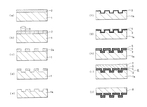
Embodiment 1
Figure 4 is a diagram illustrating the steps of
the method according to an embodiment of the present
invention.
As shown in Figure 4(a), substantially the whole
surface of a flat glass substrate 1 is coated with
photoresist 2. Laser light 9 is directed to specified
spots of the photoresist 2 to expose it (Figure 4(b)) and
the photoresist 2 is developed to form a minute pattern 2a
(Figure 4(c)). The glass substrate 1 is etched to a depth
of about 800 A at portions not masked by the photoresist
pattern 2a (Figure 4(d)). Suitable etching techniques
include physical etching, such as spatter etching, plasma
etching, ion etching, and the like (in this embodiment,
spatter etching is employed).
- . .
~205~ 7
When the etching is completed, the photoresist
pattern 2a as a mask is eliminated to form a glass master
la (Figure 4(e)).
Next, the glass master la is subjected to
sputtering in a vacuum chamber to form a first nickel layer
3 on its surface (Figure 4(f)). The first nickel layer 3
is about 500 A in thickness. After the first nickel layer
3 is formed, an intermediate layer 4 is made of tantalum
having a lower linear expansion coefficient than nickel as
the first nickel layer 3 (Figure 4(g)). The intermediate
layer 4 is about 500 A in thickness. After that,
substantially the whole substrate is subjected to
sputtering to form a second nickel layer 5 substantially
identical in thickness to the first nickel layer 3 on the
intermediate layer 4 (Figure 4(h)). As a result, a
conductive layer film 6 having a three-stratum structure
comprised of the first nickel layer 3, an intermediate
layer 4 and a second nickel layer 5, is formed on the
surface of the glass master la. The first nickel layer 3,
the intermediate layer 4 and the second nickel layer 5 are
formed successively in a vacuum chamber maintained at about
8 mtorr vacuum without contacting outside air. This
results in the layers 3, 4 and S of the conductive layer
film 6 adhering well to one another.
After that, an electroformed layer 7 is formed on
the conductive layer film 6 by an electroforming process
(Figure 4(i)). The electroformed layer 7 is formed of
nickel in a thickness of about 300 ~m. Then, the
electroformed layer 7 with the conductive layer film 6 are
separated from the glass master la (Figure 4(j)) to produce
a stamper 8. The electroforming process itself may be a
method known to those skilled in the art.
Embodiment 2
A glass master la, manufactured in accordance
with the method of Embodiment 1, is subjected to sputtering
in a vacuum chamber to form a first nickel layer 3 (Figure
4(f)) of a thickness of about 300 A in thickness. After
3 ~ 7
the first nickel layer 3 is formed, an intermediate layer
4 is formed of tantalum having a lower linear expansion
coefficient than nickel over the first nickel layer 3
(Figure 4(g)). The intermediate layer 4 may have a
thickness of about 200 A assuming, for example, that the
first nickel layer 3 is about 300 A in thickness, so that
the thickness ratio of the first nickel layer 3 to the
intermediate layer 4 may be in the range of from about 3 :
2 to 6 : 5. The whole substrate is subjected to sputtering
to form a second nickel layer 5 substantially identical in
thickness to the first nickel layer 3 on the intermediate
layer 4 (Figure 4(h)). As a result, a conductive layer
film 6 having a three-stratum structure comprised of the
first nickel layer 3, the intermediate layer 4 and the
second nickel layer 5, is formed on the surface of the
glass master la. The first nickel layer 3, the
intermediate layer 4 and the second nickel layer 5 are
formed successively in a vacuum chamber maintained at about
8 mtorr vacuum without contacting the outside air. This
results in the layers 3, 4 and 5 of the conductive layer
film 6 adhering well to one another.
The steps following the above steps to produce a
stamper 8 are all the same as those of Embodiment 1.
When the conductive layer film has a three-
stratum structure, having a thickness ratio of the firstnickel layer to the intermediate tantalum layer in the
range of from 3 : 2 to 6 : 5, the conductive layer film can
be more effectively prevented from flaking off the glass
master during the electroforming process, particularly with
a conductive layer film formed by depositing a first nickel
sublayer of a thickness of about 300 A, an intermediate
tantalum layer of a thickness of about 250 ~, and a second
nickel superlayer of a thickness of about 300 A by
spattering, much greater effect can be attained; for
example, a 100% yield has been attained in a 20 times trial
of the electroforming process. When the conductive layer
film has a thickness ratio of the first nickel layer to the
-- 10 --
~ 7J
intermediate tantalum layer outside the preferred range of
from about 3 : 2 to 6 : 5, the conductive layer film which
is formed by depositing a first nickel sublayer of a
thickness of about 300 A, an intermediate tantalum layer of
a thickness of about 400 A, and a second nickel superlayer
of a thickness of about 300 A, poor results were observed
five times among the 20 times trial of the electroforming
process with a yield of 75~.
Embodiment 3
First, as shown in Figures 5(a) to 5(c), a glass
substrate 51 is coated with photoresist 52, and is
irradiated by laser light 57 for cutting. The photoresist
52 is developed to form the desired resist pattern 52a.
Then, as shown in Figures 5(d) to 5(e), the glass substrate
51 is subjected to spatter etching at portions not masked
by the resist pattern 52a to produce a specified pattern,
and the resist pattern 52a is subsequently removed.
Then, as shown in Figure 5(f), a tantalum layer
53 is formed by sputtering. The tantalum layer 53 has a
thickness of about 300 A. Next, as shown in Figure 5(g),
a nickel layer 54 of a thickness of about 300 A is formed
by sputtering. The whole substrate is then soaked in a
solution of about 5~ by weight potassium dichromate for one
minute to form a nickel passive-state film on the nickel
layer surface. Thus, the glass master for manufacturing a
stamper is produced.
Then, as shown in Figure 5(h), the glass master
is subjected to an electroforming process to form a nickel
electroformed layer 55 of a thickness of about 0.3 mm.
After that, the nickel electroformed layer alone is
separated from the glass master to produce a stamper 56 as
shown in Figure 5(i).
Embodiment 4
In this embodiment, the glass master employed in
Embodiment 3 is reused.
Since the master board, once used, may have a
flaw in the nickel passive-state film during a purifying
_ ~,
~.
. . ,
~ 2 0 5 6 3 0 7
process after the electroformed layer is separated from the
glass master, the glass master is purified with a solution
of nitric acid, for example 20% by weight, to remove the
nickel passive-state film and nickel layer.
Following the above steps, the same steps as
those discussed for Embodiment 3 are carried out to form a
nickel layer and a nickel passive-state film, to produce a
glass master and to produce a stamper.
The resultant stamper has a good quality without
deterioration of an S/N ratio because the nickel passive-
state film of the glass master corresponding to a signal
face of the stamper is renewed every time it is used, and
substantially identical stampers can be newly produced
based upon a single glass master.
Embodiment 5
Referring now to Figure 6, a nickel-tantalum
alloy conductive layer film 69 containing tantalum in the
range of from about 3 to 10% by weight is formed in a
thickness of about 1000 A on a surface of the glass master
61a shown in the Embodiment 4, by spattering, using an
alloy target. A nickel electroformed layer is then formed
in a thickness of about 300 ~m by the electroforming
process as stated in the Embodiment 4, and the conductive
layer film is separated from the glass master 61a to
produce a stamper.
The conductive layer film is prevented from
flaking off the glass substrate during the electroforming
process by utilizing a property of tantalum tightly
sticking to the glass substrate. The conductive layer film
easily flakes off when tantalum is present in the nickel-
tantalum alloy in a concentration of less than 3% by
weight, while the conductive layer film sticks so firmly at
concentrations of tantalum greater than 10% that the
separation of the conductive layer film is impossible.
Alternatively, a conductive layer film formed of
a nickel-tantalum alloy containing tantalum at a
- 12 -
~ ~5~3~ ~
~ concentration of 3 to 10% by weight does not have the
above-mentioned problems and a good stamper can be made.
As previously mentioned, according to the present
invention, a substrate is subjected to spatter etching, ion
etching or plasma etching to form an irregular pattern, and
a conductive layer film, having a three-stratum structure
wherein a layer of metal of a lower linear expansion
coefficient than nickel is sandwiched between two nickel
layers, is formed on the substrate. In this way, the
resultant conductive layer film has a lower linear
expansion coefficient than a conventional nickel or silver
single-stratum film, a silver-nickel two-stratum film, or
a nickel-silver-nickel three-stratum film and,
consequently, the conductive layer film and substrate can
have a reduced difference between linear expansion
coefficients. Thus, the conductive layer film can be
prevented from flaking off the glass master during the
electroforming process, and a good stamper can be obtained.
Forming the first and second nickel layers of
substantially the same thickness will also prevent the
conductive layer film from bending with variations in
temperature. Furthermore, since the conductive layer film
having the three-stratum structure can be formed in a
vacuum chamber where a vacuum state is maintained without
contacting the outside air, the layers adhere well to each
other, and the electroformed layer can be separated from
the glass master between the glass master and the first
nickel layer. Thus, a stamper having a good signal face
surface accuracy and having a high quality can be obtained.
In accordance with the present invention, a
nickel electroformed layer can be formed on the glass
master without flaking the conducting layer film on the
surface of the master board and good stampers free from
deterioration of an S/N ratio can be newly produced based
upon a single master board.
- 13 -