Note: Descriptions are shown in the official language in which they were submitted.
This invention relates to a method of passivating a
semiconductor device, and a semiconductor device passivated
thereby.
Typical semiconductor devices consist of a large number
of active components formed on a substrate and include one
or two levels of polysilicon, polycide, silicide or a
combination of thereof, as well as one, two or more levels
of interconnect layers insulated by various dielectrics.
Moisture and ions of various type can have very
important negative effects on the performance and
reliability of such devices.
CMOS transistors show threshold voltage instabilities
when sodium, Na+, lithium, Li+, potassium, K+, hydrogen, H+,
hydronium, H30+, and hydroxyl, OH , ions are allowed to
approach the gate oxide area. Hydrogen, hydronium and
hydroxyl ions originate from moisture ionization.
Interconnect materials, such as aluminum alloys and
titanium-based refractory metals and compounds corrode when
electrically polarized and exposed to moisture. These
galvanic reactions occur faster when catalyst ions, such as
chlorine, C1-, are present in trace levels and when elements
like copper are used in the aluminum alloy.
Dielectrics are electrically affected by moisture. For
example, bulk resistivity reduction, electrical
polarization, hot electron effects, and slow trapping
degradation. They are also affected mechanically in that
they tend to acquire a compressive as they absorb moisture.
They can be chemically attacked as well, particularly when
alloyed with boron and phosphorus. Decomposition to boric
and phosphoric acids can result and initiate corrosion of
surrounding interconnect materials.
- 1 -
2~~~~~~~
In order to prevent moisture build-up and ion
penetration in the device, it is known to form a passivation
layer on the surface of the device. This is patterned to
permit the opening of the bond pads to which bond wires are
connected. The passivation layer also prevents conductive
particles and scratches from shorting top interconnects.
The passivation layer can be deposited from silicon,
oxygen, nitrogen, phosphorus and/or a gas containing another
metallic element by atmospheric pressure chemical vapour
deposition, APCVD, low pressure chemical vapour deposition,
LPCVD, plasma enhanced chemical vapour deposition, PECVD,
laser assisted chemical vapour deposition, LACVD, photo
assisted chemical vapour deposition, PACVD, electron
cyclotron resonance chemical vapour deposition, ECRCVD. It
can be deposited from silicon, and/or silicon nitride,
and/or silicon oxide, and/or silicon oxinitride targets,
with or without oxygen, nitrogen or any other reactive gas,
by sputtering, reactive sputtering, biased sputtering, or
reactive biased sputtering. It can also be deposited by any
combination of these techniques.
The deposited film consists of silicon oxide, which can
be alloyed with phosphorus or other metallic elements,
silicon nitride; silicon oxinitride, or combination thereof.
Since the passivation layer is deposited from the
vapour phase or by sputtering, the surface coverage is
strongly affected by the exposed solid angle of the surface
to cover. The upper topography characterized by a large
exposed solid angle receives more passivation material, and
thus produces a thicker passivation layer, than the recessed
regions with only small solid angle exposed to the vapour
from which the passivation layer grows. The net result is a
passivation surface coverage that varies with the underlying
topography and has many seems, gaps, voids and other weak
- 2 -
points.
Water vapour molecules can diffuse in the passivation
layer at a rate which is a function of its diffusion
constant, D, in the passivation material. The time, t,
needed for water to diffuse through the passivation material
is proportional to the square of the passivation layer
thickness, 82, and inversely proportional to the diffusion
constant. This means that, at any temperature and for any
concentration of moisture in the device area, a thick
passivation layer, 8T, should be much better than a thin
one, at, and the protection should increase as the square of
the passivation layer thickness increase:
~tT/tt) - ~ST/6t)z
and doubling the thickness of the passivation layer should
quadruple the resistance of these devices in any moist
ambient. In practice, increasing the thickness of the
passivation layer only gives slight improvement of device
protection because of the reduced step coverage at weak
points.
The use of a partial etchback process using a semi-
inorganic spin-or_ glass layer for a semiconductor dP«ice
passivation application has been proposed by Intel [D.
Pramanik, S. Nariani and G. Spadini, 6th Annual IEEE VMIC
Conf., Santa Clara, California, June 12-13, 1989, pp. 454-
462]. The spin-on glass was a 0.23 ~m thick siloxane that
was partially etched away using an SF6 etchback plasma in
order to remove most of the spin-on glass from the upper
topography and to leave it in crevices.
However, it was later found that these siloxane spin-on
glasses, that incorporate methyl, ~CH3, ethyl, ~C2H5,
propyl, ~C3H~, or butyl, ~C4Hg, groups connected to silicon
- 3 -
atoms in the spin-on glass solution and spin-on glass layer,
cause field inversion, leading to failure of CMOS devices.
Hydrogen from the organic groups of these quasi-inorganic
spin-on glasses is the cause of the problem. Quasi-
inorganic spin-on glasses cannot be used in passivation
applications, particularly when a high hydrogen content
plasma silicon nitride is deposited over the spin-on glass
layer. The hydrogen from the silicon nitride and spin-on
glass layers would interact and cause threshold voltage
instabilities. Generally speaking, organic materials should
be avoided in sensitive CMOS devices.
Since these quasi-inorganic spin-on glasses are not
thermally stable at temperatures higher than about 450°C,
the use of ceramic packages is very difficult. Furthermore
as the quasi-inorganic spin-on glasses are readily destroyed
during oxygen plasma exposure, dry photoresist strip is not
possible. Saturation of the passivation layer with moisture
may occur during wet photoresist strip.
Consequently attempts to avoid the problems caused by
variations in thickness of the passivation layer by using
spin-on glass have not been successful.
Ar_ object of the present invention is to alleviate the
afore-mentioned disadvantages of the prior art.
According to the present invention there is provided a
method of passivating a semiconductor device, comprising
depositing a first dielectric passivation layer on the
surface of the device, forming at least one planarization
layer over said first passivation layer from an inorganic
spin-on glass solution containing organometallic molecules
of X and silicon, where X is selected from the group
consisting of phosphorus, arsenic and antimony, said spin-on
glass solution being pre-reacted to form at least one Si~O~X
- 4 -
bond between said organometallic molecules of silicon and X,
and subsequently depositing a second dielectric passivation
layer on said at least one planarization layer.
Preferably, X is phosphorus.
By using a passivation sandwich, including an inorganic
SOG (spin-on glass) planarization layer, the problems caused
by varying thickness of the passivation layer can be
substantiially reduced.
The inorganic spin-on glass solutions used in the
present invention can be applied in a non-etchback process.
They are doped with phosphorus and contain silicon and
phosphorus organometallic molecules diluted in various kind
of solvents and alcohols. These silicon and phosphorus
organometallic molecules are pre-reacted in the solution in
order to form at least one and preferably two or more
silicon-oxygen-phosphorus, Si~O~P, bonds between phosphorus
atoms of the phosphorus organometallic molecules and silicon
atoms of the silicon organometallic molecules. The obtained
phosphorus and silicon organometallic molecules are
independent and in liquid solution in the solvent mixture
but already connected by at least one and preferentially two
Si~O~P bonds prior to spinning, The silicon o_rganometallic
molecule is tetraethylorthosilane, TEOS. The commercial
names of two such spin-on glass solutions are Accuglass P-
062A and Accuglass P-062LS, manufactured by Allied-Signal,
Milpitas, California, USA.
Two similar solutions are manufactured by Filmtronics,
~:; Butler, Pennsylvania, USA and Tokyo Ohka Kogyo, Gotenba,
JAPAN. These solutions are respectively named by their
manufacturer as P-062F and OCD-2P-37313-SG. These two
phosphosilicate solutions, however, as is the case for any
other solution having the same characteristics, are not
- 5 -
suitable for use in the present invention because of an
inadequate pre-reaction of the spin-on glass solution and/or
because the phosphorus organometallic molecule do not permit
the formation of at least one and preferably two or more
~Si~O~P~ bonds between phosphorus atoms of the phosphorus
organometallic molecules and silicon atoms of the silicon
organometallic molecules. For these solutions, Si~O~P bonds
only form during spin-on glass film curing and the obtained
phosphorus doped silicate film has poorly bonded phosphorus,
prone to leaching and prone to form phosphoric acid in
presence of moisture.
The phosphorus organometallic molecule, the silicon
organometallic molecule, TEOS, water and the various
alcohols, schematized as R~O~H in the following figure, are
then pre-reacted in order to obtain, in the spin-on glass
solution, complex organometallic molecules, of about 1000 to
5000 u.m.a. of molecular weight, in suspension in the
solution containing water, alcohols, and catalyst acids.
The various alcohol molecules form Van der Waals bonds with
the peripheral silanol bonds, ~SiOH, thus blocking silanol-
silanol condensations that would result in an increase of
the compound molecular weight and of the water content in
the solution:
H
R H ~ C ~ H R
O ~ ~ H H ~ C ~ H H ~ ~ O
R H ~~ O O O ~~ H R
O ~ ~ H Si ~ O ~ Si ~ O ~ H H ~ ~ O
;:,
H H H ~ ~ O O R O O ~ ~ H
H ~ C ~ C ~ O ~ Si H ~ ~ O Si ~ O ~ Si ~ O ~ H
H H O O ~ ~ H O O H H
H ~ O ~ P ~ O ~ Si ~ O ~ Si ~ O ~ C ~ C ~ H
- 6 -
~~~~~~5~
R ~ O ~ H O O O R H H
H ~ C ~ H Si H ~ ~ O
H ~ C ~ H O O O ~ ~ H
H Si ~ O ~ Si
H ~ ~ O O ~ ~ H O ~ ~ H
O ~ ~ H H ~ ~ O H ~ ~ O
R R R
During coating and spinning over the previously
deposited dielectric film, solvents and water evaporate and
spin-on glass polymerisation occurs as a result of the
condensation of silanol pairs, thus resulting in the
formation of excess water, which evaporates. Polymerization
of the spun film stops when the distance between
neighbouring silanol groups becomes too large or when too
much by-product, such as water vapour, blocks the
condensation mechanism. Heating is then required to
eliminate condensation by-products and permit further
condensation, densification, and the formation of a hard
phosphorus doped inorganic layer, i.e. the SOG layer.
As mentioned in our Canadian co-pending patent
application no. 2,006,174, a non etch-back multiple coating
sequence, using two or more layers of spin-on glass, is
needed in order to prevent film cracking. An in-line cure
to a temperature of at least 300°C and preferably at least
350°C is also needed in order to insure silanol-ethoxy
groups, ~SiOH - ~SiOC2H5, condensation, important film
shrinking and ethanol evaporation between each coat.
As mentioned in our patent application no. 2,017,719
during, between, and after each one of the multiple coats of
spin-on glass, the silicon wafer is transported, cured and
stored in a moisture-free ambient in order to prevent water
_ 7 _
molecules from breaking Si~O~P bonds upon processing.
As mentioned in our patent application no. 2,017,710,
the final multiple coats spin-on glass layer is in-situ
cured in a dry ambient or preferably in a vacuum at
temperatures of about 425°C for about one hour priar to the
deposition of the upper protective dielectric.
As mentioned in our Canadian patent application no.
entitled "CURING AND PASSIVATION OF SPIN-ON GLASSES BY A
PLASMA PROCESS, AND PRODUCT PRODUCED THEREBY", it is
possible to more efficiently cure the spin-on glass layer of
wafers located on one or more electrodes of a plasma reactor
by using the electrical field generated near the surface of
the wafer by the inert or reactive gas glow discharge. This
curing sequence is particularly attractive and efficient
when the upper protective layer is a plasma deposited film
deposited in a vacuum load-locked parallel plate reactor as
the case for PECVD SiN in a NOVELLUS reactor.
The final density of the spin-on glass layer depends on
many factors but is generally lower than the density of
other inorganic glasses deposited by other commonly used
techniques like LPCVD or PECVD. This lower density is due
to the presence of many pores in the spin-on class layer
which cause high conductance channelling paths between the
spin-on glass surface and its bulk.
These pores permit the adsorbed gas molecules present
on the SOG film surface to continuously and rapidly diffuse
through the bulk of the film and to rapidly connect
physically to the glass by forming low energy (<0.1 eV) Van
der Waals bonds (shown as "~~"). The gas molecules are
rapidly absorbed physically by the SOG film network.
Water vapour can slowly form high energy (>0.1 eV)
_ g _
2~ s~~~~
chemical bonds (drawn as "~" on the following diagram) with
the SOG film network by forming a pair of silanol groups,
~SiOH. Ater is slowly chemically absorbed by the SOG film
network:
Si O Si O O Si O Si O O
O O H Si O O Si
Si O O O Si H O O
O H Si - O H O Si
Si O O O Si 0 O O
.
O Si Si O O Si Si
Si O O O Si O O O
This slow chemical absorption of water vapour by the
SOG film is particularly efficient if the SOG solution
contains phosphorus organometallic molecules which give very
efficient water vapour gettering due to the presence of
phosphorus-oxygen double bounds in the SOG film:
' 25
Si O Si O
O Si O H Si
Si H O O Si O O O
O O O P O Si O - O P O Si C
.
Si H O O Si O O O
O Si O H Si
Si O Si O
Our recent patent Canadian application nos. 2,027,720
and 2,023,172 show that these physical and chemical
reactions involving water vapour and ~P:O or ~SiOSi~ bonds
_ g _
are reversible ones at relatively low temperature. The
spin-on glass layer is easily dried if exposed to a dry
ambient or preferably a vacuum at temperatures of about
425°C for a time sufficiently long to permit:
(1) Slow chemical desorption, or destruction of
chemical bonds with the glass network,
(2) Rapid physical desorption, or destruction of the
Van der Waals bonds with the glass network,
(3) Rapid diffusion from the bulk to the surface
l0 through adjacent pores, and
(4) Rapid desorption from the surface
The obtained spin-on glass layer is dry and, as
mentioned in our recent Canadian patent application no.
2,032,763, contains less hydrogen then typical vapour
deposited phosphosilicate layers that are normally used as
passivation layers.
Spin-on glass layer exposure to moist air causes
extremely rapid readsorption of water vapour at the film
surface, rapid ~iiff~lci~n frnm ~pra_ tp more, rapid r~rysir_al
reabsorption and chemical reabsorption. Since the spin-on
glass layer is more porous than the surrounding vapour
deposited glasses and since the pores of the spin-on glass
layer are normally under vacuum, the spin-on glass layer
will very rapidly absorb more water vapour, as bonded H2o,
and chemically absorb more of it, as ~SiOH groups, than its
equivalent volume of vapour deposited glasses when exposed
to air or to a pressure cooker ambient. The same way, since
the spin-on glass layer incorporates phosphorus, water
vapour will also be chemically bonded as ~POH groups.
- 10 -
,.
Being more active than for moisture absorption, the
spin-on glass layer will then protect the surrounding
dielectrics against moisture absorption and, for any given
moisture load, will maintain higher their bulk resistivity.
The resulting device, which incorporates a dry spin-on
glass layer, will have an improved barrier against water
vapour penetration to device transistors during highly
accelerated stress testing (HAST), temperature and humidity
bias testing (THB), other reliability testing, or simply in
the field.
The first layer can be deposited by atmospheric
pressure chemical vapour deposition, APCVD, low pressure
chemical vapour deposition, LPCVD, plasma enhanced chemical
vapour deposition, PECVD, laser assisted chemical vapour
deposition, LACVD, photo assisted chemical vapour
deposition, PACVD, electron cyclotron chemical vapour
deposition, ECRCVD, sputtering, biased sputtering, reactive
sputtering, or any combination of these techniques. Plasma
enhanced chemical vapour deposition, PECVD, is preferred.
This first layer can be silicon dioxide, stoichiometric
or not, doped or not with metallic elements like phosphorus.
It can be si.l.icon nitride, stoichiometric or not, or silicon
oxinitride. It can also be a combination of these
materials. Undoped and stoichiometric silicon dioxide is
preferred. The thickness of this first dielectric layer is
about 0.2 to 1.0 ~Cm and preferably 0.5 ~Cm.
The equipment used for the deposition of this first
dielectric layer can be a single wafer machine, a batch
machine, and can be independent or integrated to the spin-on
glass processor that is used for the spin-on glass
deposition.
- 11 -
The spin-on glass solution used is a phosphorus doped
spin-on glass solution that permits the formation of a film
having about 1.0 to 5.0 wt% and preferably 2.0 wt%
phosphorus, after a final cure at about 425°C. The
phosphorus atoms contained in the complex organometallic
molecules of the spin-on glass solution are bonded to the
silicon atoms of these complex organometallic molecules by
at least one and preferably more than one Si~O~P bond(s).
The thickness of a single coat spin-on glass film
obtained after spinning at a speed of rotation of 4000 RPM
for about 20 seconds, at a temperature of about 21°C, and a
relative humidity of about 40% RH is about 35 nm to 150 nm,
preferably 75 nm thick.
The coated wafer is preferably transported from the
spin area to the first in-line hot plate in a nitrogen dry
ambient. The nitrogen dry ambient will be maintained up to
the transfer to the second dielectric deposition equipment
that is used to deposit the top layer which protects the
multiple coat spin-on glass layer).
The wafer can be automatically transported in the dry
nitrogen ambient through successive hot plate stations in
order to evaporate residual solvents, to evaporate residual
moisture, to permit the condensation of fad neighbouring
silanol groups which results in the formation of more water
to evaporate, to permit an efficient condensation of ethoxy
groups with neighbouring silanol groups which results in the
formation of more ethanol to evaporate, and to insure a
gradual volumetric contraction.
The temperature of these various hot plates increases
from the first to the last, the first one being at a
temperature lower than 120°C and preferably 80°C while the
last is at a temperature of at least 300°C and preferably
- 12 -
350°C or higher. The ambient around these hot plates is dry
nitrogen.
After completion of the in-line cure, each wafer is
cooled in a dry nitrogen ambient and sent back to the
coating area for the addition of another coat and for
another in-line cure cycle.
After completion of this multiple coats and in-line
cures sequence, which can accumulate between two and five,
and preferably four coats of spin-on glass, the wafers are
rapidly transferred to the independent or integrated
equipment that is used to deposit the top protective layer.
Minimization of air exposure is important for an independent
equipment and, for that reason, a dry nitrogen or vacuum
transport mechanism to an integrated equipment is preferred.
The independent or integrated equipment permits an in-
situ final cure prior to the deposition of the top
protective layer. The role of this in-situ cure is to dry
the spin-on glass layer by condensing as much as possible
the silanol groups and to evacuate as much as possible the
water vapour.
The top protective layer can be deposited by
atmospheric pressure chemical vapour deposition, APCVD, low
pressure chemical vapour deposition, LPCVD, plasma enhanced
chemical vapour deposition, PECVD, laser assisted chemical
vapour deposition, LACVD, photo assisted chemical vapour
deposition, PACVD, electron cyclotron chemical vapour
deposition, ECRCVD, sputtering, biased sputtering, reactive
sputtering, or any combination of these techniques. Plasma
enhanced chemical vapour deposition, PECVD, is preferred and
an in-situ plasma cure of the spin-on glass, as described in
our patent application: "CURING AND PASSIVATION OF SPIN-ON
GLASSES BY A PLASMA PROCESS, AND PRODUCT PRODUCED THEREBY",
- 13 -
~~ ~~~~~L,
is preferred.
The second layer can be silicon dioxide, stoichiometric
or not, doped or not with metallic elements like phosphorus.
It can be silicon nitride, stoichiometric or not, or silicon
oxinitride. It can also be a combination of these. A
plasma enhanced chemical vapour deposited silicon nitride
deposited at a temperature lower than about 450°C and having
a compressive stress lower than 2.0 E9 dynes/cmz and a
concentration of Si-H bonds lower than 4.0 E21/cm3 being
preferred. The thickness of this second dielectric layer is
about 0.5 to 1.5 /gym and preferably 1.0 ~,m.
The invention will now be described in more detail, by
way of example only, with reference to the accompanying
drawings, in which:-
Figure 1 shows a semiconductor double level
polysilicon, single level interconnect prior to the
application of a passivation layer;
Figure 2 shows the device shown in Figure 1 with a
passivation layer applied in accordance with the prior art;
Figure 3 shows the effect of increasing the thickness
of the passivation layer in the device shown in Figure 2;
Figures 4a and 4b illustrate the steps in forming a
spin-on glass passivation sandwich in accordance with the
invention;
Figure 5 is a diagram of a comb arrangement used to
verify the performacne of a passivation layer;
Figures 6a and 6b show two underlying strucures for the
comb arrangement;
- 14 -
r ~. z~
Figures 7a to 7c are diagrams showing the leakage
current for single, double, and SOG-sandwich passivation
layers as deposited measured by the first comb structure,
i.e. without a SOG undrlayer;
Figures 8a to 8c are diagrams showing the leakage
current for single, double, and SOG-sandwich passivation
layers measured by the second comb structure, i.e. with a
SOG undrlayer;
Figures 9a to 9c show similar results to Figures 7a to
7c after one hour in a pressure cooker;
Figures l0a to lOc show similar results to Figures 8a
to 8c after one hour in a pressure cooker;
Figures lla to llc show similar results to Figures 7a
to 7c after ten hours in a pressure cooker;
Figures 12a to 12c show similar results to Figures 8a
to 8c after ten hours in a pressure cooker.
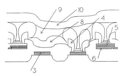
Referring now to the drawings, the semiconductor device
shown in Figure 1, which is shown prior to the application
Cf a paSSlVatl.On layer, CQmpriSec a ci 1 i Cpn S~~hSt'_'atc 1, 3
field oxide 2, polysilicon, silicide or refractory metal
gate 3, and contact 4 to a capacitor electrode, gate or the
silicon substrate. Upper and lower capacitor electrodes 5,
6 are made of polysilicon, polycide or refractory metal.
The device is planarized with a reflowed BPSG layer or a
spin-on glass layer 7.
When the passivation layer 8 is applied using
conventional techniques, the result is shown in Figure 2.
The surface coverage varies, with many seems, gaps, voids
and other weak points formed in the layer 8.
- 15 -
;fir-,~ ~~
Figure 3 shows what happens when the thickness of the
passivation layer is increased. Only minimal improvement in
the performance of the device is observed due to reduced
step coverage at weak points 8a.
The fabrication of a device in accordance with the
invention will now be described with refernce to Figures 4a
and 4b. First, a conventional passivation layer is
deposited by vapour phase deposition onto the partly
completed device shown in Figure 1 to produce a device as
shown in Figure 2. Next, a phosphorus-doped, inorganic
spin-on glass layer 9, such as Accuglass P-062A,
manufactured by Allied-Signal, Milpitas, California, USA, is
applied and cured in one or many coats over the deposited
first layer 8. While phosphorus is preferred, the invention
could also be made to work with arsenic or antimony. This
SOG layer fills crevices and ensures a smooth upper surface.
Finally, another passivation layer 10 is deposited by
vapour phase deposition onto the SOG layers) 9. The
resulting sandwich has few or no weak points. The
passivation layer thickness is equal or larger than the
combined thickness of the two vapour phase deposited films.
Since the SOG approach. prevents the formation of weak
points by ensuring a minimum thickness of at least the sum
of the two vapour deposited layers' thickness, it is much
more effective than that employing double thickness vapour
deposited passivation.
The use of an inorganic spin-on glass solution
containing phosphorus and silicon organometallic molecules,
with the spin-on glass solution being pre-reacted to form at
least one Si~O~P bond between said phosphorus and silicon
organometallic molecules, avoids the moisture problems noted
above.
- 16 -
Since the bulk resistivity of dielectrics degrades
rapidly in presence of moisture, the performance of the
standard passivation layer, of a double thickness
passivation layer and of the SOG passivation sandwich can be
verified by monitoring the leakage current between two
independent combs (see Figure 5) as the moisture content
over the passivation layer is increased.
Two underlying film structures A, B were used in order
to verify the leakage current between the two independent
combs. In the first case, structure A, (Figure 6a), the
combs 20, formed by an interconnect layer, sit on a field
oxide 21 grown from the underlying substrate 22. In the
second case, structure B, (Figure 6b), the comb 20 sits on a
spin-on glass layer 23 deposited over a field oxide 21
previously grown from the underlying substrate 22.
Electrical testing of the leakage current between the
two independent combs is performed at a bias of 100 volts
applied between bond pads 15, 16 (Figure 5). This voltage
induces an electrical field of 0.5 MV/cm in the dielectric
material that insulates the two combs. When completely dry,
this insulating dielectric has a bulk resistivity of about
1. OE+16 n.cm. The penetration of moisture in the dielectric
area causes this bulk resistivity to be reduced by many
orders of magnitude. The leakage current monitoring can
trace this penetration.
Since the two independent combs are 0.8 um thick, since
they are isolated by about 2.0 ~Cm of dielectrics, since
their total exposed length is about 349958 ~Cm per structure
(994.2 ~m/arm x 2 arm/pitch x 88 pitches/comb x 2
comb/structure), then the leakage current should be about
0.1 pA or -1.0 on a log scale in pA units.
About 172 measurements of the inter-comb leakage
- 17 -
current were performed and plotted on a log scale (in pA):
1). For each one of the two wafer structures:
structure A, without underlying SOG layer, structure B, with
an underlying SOG layer under the pair of combs in order to
increase the leakage current for the same moisture
penetration,
2). For each one of the three tested passivation
layers: simple passivation, which is a single thickness
layer of the standard passivation material, double
passivation, which is a double thickness layer of the
passivation material, SOG passivation, which is a
combination of a passivation layer deposited under a spin-on
glass film, which is spun under another passivation layer.
The cumulative thickness of this SOG passivation, is similar
to one of the double passivation layer.
3). For three test conditions: as deposited, which
means after completion of the device and without any
intentional moisture exposure, after one hour of pressure
cooker at 121°C and about 180 kPa of moisture, and after ten
hours of pressure cooker at 121°C and about 180 kPa of
moisture.
The leakage current (about 1 000 pA or 1 nA) associated
with the as-deposited structure A (without SOG underlayer)
using single passivation and double passivation (figures 7a,
7b) shows that this type of passivation is not adequate to
prevent residual moisture absorption from moist air of the
manufacturing area. A three order of magnitude lower
leakage current (about 2 pA) is associated with the improved
step coverage of the SOG passivation (Figure 7c) and
confirms that this improved step coverage eliminates
residual moisture.
- 18 -
The residual moisture effect is even more spectacular
in the case of as-deposited structure B (with SOG
underlayer) because the bulk resistivity of SOG in presence
of moisture drops much more quickly than the one of field
oxide. In this case, single passivation and double
passivation (Figures 8a and 8b) show a higher leakage
current (about 50 000 pA or 50 nA) while the leakage current
of the SOG passivation (Figure 8c) stays ten thousand times
lower (about 2 pA). This second structure is much more
sensitive for the detection of moisture in dielectrics.
A one (1) hour pressure cooker exposure at 121°C and
175 kPa causes moisture penetration in the dielectrics and
increases inter-comb leakage current if the passivation is
not absolute. The high leakage current (about 50 00o pA or
50 nA) associated with the structure A after one hour in a
pressure cooker (without SOG underlayer) using single
passivation (Figure 9a) shows the permeability of this
passivation. The comparable leakage current (about 10 000
pA or 10 nA) associated with double passivation (Figure 9b)
shows that the improvement of a double thickness is minimal,
as predicted by the step coverage discussion. A three order
of magnitude lower leakage current (about 50 pA) is again
associated with the SOG passivation (Figure 9c) and shows
the beneficial effect of the improved step coverage of the
SOG.
The step coverage effect is spectacular in the case of
structure B after one hour in a pressure cooker. In this
case, single passivation and double passivation (Figures l0a
and 10b) show almost the same leakage current (about 300 000
pA or 0.3 ~cA) while a ten thousand times lower leakage
current (about 10 pA) is maintained with the SOG passivation
(Figure lOc). When compared with the 300 000 pA leakage
current of these single passivation and double passivation,
the 10 pA leakage current of the SOG passivation is probably
- 19 -
the most convincing indication of the high performance due
to the improved step coverage of the SOG passivation.
A ten (10) hours pressure cooker exposure at 121°C and
175 kPa causes even larger moisture penetration in the
dielectrics and increases even more inter-comb leakage
current. The high leakage current (about 250 000 pA or 0.25
~CA)associated with structure A using single passivation
(Figure lla) and the comparable leakage current (about 100
000 pA or 0.1 ~A) associated with double passivation (Figure
llb) again shows that the reduced step coverage and weak
points of a double thickness passivation cause the
improvement to be minimal. The SOG passivation (Figire llc)
maintains a three order of magnitude lower leakage current
(about 100 pA).
In the case of the more sensitive structure B after ten
hours in a pressure cooker, single passivation and double
passivation (Figures 12 a and 12b) show almost the same high
leakage current (about 300 000 pA or 0.3 ~A) while the
leakage current of the SOG passivation (about 10 000 pA or
10 nA) shows the first signs of important moisture
penetration in the inter-comb dielectric area.
Structure B was only used as a very sensitive
demonstration vehicle. In a real semiconductor device, the
first level interconnect is deposited over a high density
and high temperature dielectric of similar quality as the
field oxide and, for that reason, the results of structure
#1 are more realistic.
These results indicate that the improved step coverage
of the SOG passivation over underlying topography permits
much better protection against moisture related degradation
than standard vapour phase deposited passivation layers or
thicker such passivation layers.
- 20 -