Note: Descriptions are shown in the official language in which they were submitted.
FIELD OF THE INVENTION
The present invention is directed to signal quality
monitors for electronic digital transmission systems and in
particular to channel quality monitors which can provide automatic
detection and identification of degradations in digital
communication channels.
BACKGROUND OF THE INVENTION
The goal of any communication system is to provide
reliable service to the customer or end user. However, channels
in electronic data transmission systems may become degraded due to
stress on the system. In satellite communication (SATCOM)
systems, for instance, stress can be imposed by transmitter/
receiver degradations or failure and by out-of-tolerance
conditions such as antenna pointing error, oscillator frequency
drift, etc. Other types of stress may also be imposed on the
system by precipitation occurring in a terrestrial microwave or
satellite communication link, by interference from other sources,
noise and items which may cause signal fading. The ultimate
effect of communication stress is degraded signal quality or even
complete outage. In a full duplex communication system employing
digital data modulation (PSK or FSK), the quality or reliability
of the system may be expressed in terms of an error rate which is
the number of erroneously digital pulses received per unit of
time.
The detection and identification of various functions of
a communication system are usually performed independently by a
r 1 _
collection of automated monitors which measure various signal
parameters (signal level, noise power, transmitted power, etc.)
along the signal path, as well as providing indications of the
health of various subsystems. The signals from the monitors are
compared against nominal values and stress is considered to be
detected when a sufficient amount of degradation has occurred in
one or more of the monitors. Several monitors are required to
perform any effective stress detection since each monitor only
responds to a subset of potential stresses. However, once
communication stresses have been detected, a larger number of
monitors is generally required to provide sufficient
identification of the type of stresses present. Often, more than
10 different monitors may be required to reasonably identify the
stresses common to a given link. Logic rules are then used to
combine the indications given from each monitor in order to
provide an estimate of the type of stress that the system is
undergoing.
The Bit Error Rate (BER) is an absolute measure of a data
channel's performance and automated BER monitors are available
that can be used to detect the presence of communication stress.
However, the time required to observe a single error is very long
since a nominal BER may be as low as 10-~~ bits per second.
Furthermore, monitoring the BER directly provides no warning when
slight degradations are taking place. Using BER monitors,
communication system controllers can only become aware of any
performance degradation after it already occurred, at which point
the customers would have also detected it. Monitoring the BER,
- 2 -
Gal ~ :~ ~ t
nevertheless, is still important since it represents the quality
of the end product of any communication system.
A technique known as Pseudo Error Rate (PER) monitoring
has been developed that provides earlier indications of
degradations than a BER monitor. Several types of PER monitors
are described in U.S. Patents 4,188,615 and 4,034,340. PER
monitors are now almost always included in the set of monitors
used for detection and identification of stresses. The PER
monitors overcome the long time intervals associated with BER
monitors by making use of a second, parallel, receiver channel
which is considerably degraded with respect to the main channel.
Error rate estimates are, as a result, performed much quicker in
the degraded channel due to the much large number of errors
occurring in that channel. However, that error rate is still
indicative of degradations in the main channel since it is
mathematically related to the actual error rate in the main
channel. Therefore, the PER monitor can be considered as having a
"gain" over a BER monitor since it amplifies the actual error rate
and hence is much more responsive to slight changes in signal
quality. Construction of a parallel receiver channel with a
higher noise level than the main channel is, however, a rather
expensive proposition.
Degraded parallel receiver channels can be simulated
quite easily. Consider the well-known Eye Diagram, for instance,
that is formed from the matched filtered outputs of a simple
binary communication system. The signals are sampled at times
equal to multiples of the symbol period T with positive values
- 3 -
indicating the reception of one symbol while a negative sample
indicates reception of the other symbol. The celebrated Eye
Diagram results if the matched filtered outputs are collected over
several symbol periods. The greater the eye opening is at the
centre of the symbol period where samples are taken, the better
the quality of the channel. An undistorted eye results for a no
stress, noiseless case. However, the eye becomes distorted with
the addition of noise and other communication stresses and, at the
same time, the BER increases accordingly. Trained experts
currently monitor links manually and rely heavily on Eye Pattern
monitors which display the Eye Diagram on an oscilloscope.
Although this type of monitor can provide much of the required
accuracy, it has been mainly limited to manual observation and
interpretation.
One way of simulating a degraded receiver channel was
proposed in U.S. Patent 3,721,959 by Robert A. George. The PER
monitor disclosed in U.S. Patent 3,721,959 counts the number of
times an eye trace falls within the band around a symbol detection
threshold, whereas a BER monitor counts the number of times an eye
trace crosses that symbol threshold at the sampling instants over
a given length of time. In other words, a BER monitor would
detect when the eye is completely closed at the sampling instants
whereas a PER monitor, as described in U.S. Patent 3,721,959,
would detect a partially closed eye at the sampling instants.
This results in error rate amplification for that type of PER
monitor.
- 4 -
~s~~ ~~'~:~
There are a number of limitations with conventional
automatic stress monitoring systems. First, the accuracy of
current detection and identification monitoring systems needs to
be considerably improved for satellite communication links.
Greater error rate amplification is now required than PER monitors
can currently provide for modern communication systems, which
systems have an ever increasing complexity and bandwidth. In
addition, the cost and complexity associated with multi-monitor
systems may make it difficult to justify installing these monitors
in small scale communication systems, especially if stress
identification is required in addition to detection.
SUMMARY OF THE INVENTION
A digital signal transmission channel degradation monitor
for determining communication stress in a digital transmission
channel, according to one embodiment of the present invention,
comprises a degradation detector having means for generating an
eye pattern's analog signal for a received data signal and
applying that eye pattern signal to a grid containing a number of
cells, the cells being located within boundaries of an ideal eye
pattern, a number of the cells being identified with a
predetermined arbitrary generalized pseudo error region with all
of the cells being formed by predetermined voltage amplitude
levels within the ideal eye pattern's voltage level outermost
extents and predetermined time periods within the ideal eye
pattern's period, tlue detector further comprising means for
determining when an eye trace of the generated eye pattern's
- 5 -
analog signal is located within particular cells, means for
obtaining the number of times an eye trace is in each cell of the
grid during a predetermined period of time, the numbers from all
cells being applied to a complex integrator which provides means
for performing a weighted integration and transformation of said
numbers to obtain a test statistic, means for comparing said test
statistic with a predetermined threshold value and means for
indicating a stress condition when said test statistic exceeds
said predetermined threshold value during that predetermined
period of time.
In further embodiments, the monitor also includes a
degradation classifier to identify the types of degradation or
stresses to which a channel is being subjected.
BRIEF DESCRIPTION OF THE DRAWINGS
The following detailed description of the invention will
be more readily understood when considered in conjunction with the
accompanying drawings, in which:
Figure 1 to 1d illustrate the formation of an Eye Diagram
for a simple communication signalling scheme;
Figure 2 to 2d illustrate Eye Diagrams for four different
types of operating conditions or stress;
Figure 3 is an Eye Diagram which illustrates a
transmitted signal that is sufficiently attenuated, or contains
noise, such that the signal transgresses into a forbidden zone or
window as described in U.S. Patent 3,721,959;
- 6 -
." ~p ~~ ,.;
~~_1~.~~~
Figure 4 shows an ideal Eye Diagram quantized into a grid
of cells according to the present invention;
Figures 5a and 5b show a block diagram of a logic circuit
for a monitor according to the present invention which circuit
performs automatic formation of the Digital Eye Diagram:
Figure 6a to 6d show examples of digitized eye diagrams
for four different stress conditions;
Figure 7 shows a block diagram of the channel degradation
monitor circuit according to the present invention which includes
both stress detection and identification sections; and
Figure 8a to 8d show a detailed circuit of the Complex
Integrator in Figure 7 along with three spec ific implementations.
DESCRIPTION OF THE PREFERRED EMBODIMENTS
The eye pattern type of monitor has been used extensively
to monitor communication systems. This type of monitor
simultaneously displays the received signals from a number of
signalling intervals on an oscilloscope. An indication of the
presence of almost all types of faults can be obtained by properly
interpreting the resulting waveform. The major shortcoming of
this method lies in the fact that it has essentially been limited
to a manual operation since a careful and detailed analysis of
many features of the displayed waveform is required. Many other,
nonmanual, types of monitors can be regarded as automated
implementations of certain features of the eye pattern waveforms.
Figure 1 illustrates the formation of a typical Eye
Diagram for a simple communication signalling scheme showing in
2o~ss ~9
Figure 1(d) an ideal Eye Diagram that would be obtained for an
infinite signal-to-noise ratio (SNR) and a distorted Eye Diagram
for a disturbed signal. Messages are decoded by sampling the
matched-filtered signal in Figure la at times equal to multiples
of the symbol period T with positive values indicating the
reception of one symbol and negative samples the reception of the
other signal. Collecting and overlaying matched filtered output
signals from successive symbol periods result in Eye diagrams as
shown in Figure 1(d) for both an undistorted and a distorted
signal. The properties of the Eye Diagram provide an accurate
means to identify and measure the amount and types of stress in a
communication system. Consider the Eye Diagrams shown in
Figure 2, for instance, which Eye Diagrams were simulated for a
noncoherent frequency shift keyed (NFSK) satellite communication
system under four different types of stress conditions. The first
case (a) shows a resulting Eye Diagram for a nominal 26 dB SNR
operation while the second case (b) illustrates how the effects of
a noise stress on the system deteriorates the Eye Diagram for a
case under a degraded 16 dB SNR stressed condition. The third
case (c) shows an Eye Diagram for a system subjected to a bit sync
error stressed condition and the fourth case (d) illustrates an
Eye Diagram for a case which is subjected to stress caused by a
frequency drift in the transponder local oscillator (LO).
It is clear from Figure 2 that the Eye Diagram can
provide a very effective means for monitoring stresses but has
had, up to now, a major shortcoming in that it has been mainly a
manual operation. However, a new automated stress monitor
_ g _
according to the present invention and referred to as a Digital
Eye Gridded Receiver with Arbitrary Degradation (DEGRAD) Monitor
combines the performance of the Eye Pattern Monitor and the most
general PER Monitor. This new DEGRAD Monitor automates monitoring
of the Eye Diagram and provides a means to simulate any arbitrary
degraded receiver providing a basis for any generalized pseudo
error monitor. The error amplification improvement occurs because
the simulated degraded receiver can be matched to any particular
stress, or set of stresses, by defining a particular type of
generalized pseudo error region across the entire symbol period.
An arbitrary generalized pseudo error region is shown in
Figure 2c. The error amplification is obviously greater for the
generalized pseudo error region, a cross shaped region in this
example, than for a typical PER band at the optimum sampling
instant 1/2 way across the symbol interval, the PER band having
only upper and lower levels. No eye traces fall within the PER
band shown in Figure 2c but eye traces do fall within the cross
shaped general pseudo error region.
Figure 3 illustrates the operation of a degradation
detector of the type described in U.S. Patent 3,721,959.
Envelope 12 represents an ideal Eye Diagram, the eye pattern being
an analog response resembling an eye as displayed on an
oscilloscope in which the period T of the eye pattern corresponds
to the time period of a digital pulse in a signal. When the pulse
signal loses strength, through attenuation, the eye pattern tends
to collapse towards 0 amplitude as illustrated at 16.
Furthermore, if the received pulse signal contains a substantial
- 9 -
2fl~~~'~ ~
amount of noise, this noise will be displayed on the eye pattern.
The detector described in U.S. Patent 3,721,959 defines a
forbidden zone or window 14 within the eye pattern wherein the eye
pattern signal 16 is deemed unreliable and in error if, for any
reason, the signal transgresses within window 14. The window 14
is defined in height by a high voltage reference "Vh~9h" and a low
voltage reference "V~oW" which establish the voltage excursion
limits far an acceptable signal. The window 14 is further defined
by the time period between a time T~ and time TZ which are related
to the eye pattern crossover point time To and the period T,
whereby the window is centred within the eye pattern. In the case
where the signal 16 transgresses into the forbidden region 14 due
to attenuation of the signal, this transgression can be detected
and an error signal generated. Similarly, an error signal can
also be generated when the signal has been degraded by the
presence of noise to the extent that the signal enters within the
forbidden zone 14. This type of arrangement can be used to detect
only certain types of errors because the forbidden region is
restricted to be rectangular. Errors occurring near the centre of
the symbol interval and those occurring near the edges of the
symbol interval cannot, as a result, be detected reliably with the
same forbidden region.
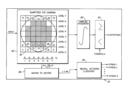
The DEGRAD Monitor 50 according to the present invention,
which is shown in Figure 7, can be used to automatically monitor a
number of stress conditions reliably because it can incorporate
any arbitrary generalized pseudo error of forbidden region. Its
principal of operation is illustrated in Figure 4 wherein the
- 10 -
4~:~h,."'~~
analog baseband filter outputs that form the Eye Diagram are
overlaid onto a quantized grid 30 for an ideal eye pattern 18.
Figure 4 shows an ideal or general eye pattern 18 quantized onto a
7 x 7 grid 30, although any grid density could be used. A timing
clock TC is used to define each horizontal increment in the grid
while a set of voltage levels ("level 0" to "level 7" in this
case) are used to define each vertical increment so that the
timing clock and voltage levels will define each cell in the
7 x 7 grid. Each cell is identified as shown in Figure 4 with
cells 11 to 17 being defined by voltage levels between 0 and 1 and
timing clock periods 1 to 7. Cells 71 to 77 are defined by
voltage levels between 6 and 7 and timing clock periods 1 to 7.
An arbitrary generalized pseudo error region within pattern 18 can
be defined by using a number of cells to form that region, for
instance cells 23 to 25, 32 to 36, 42 to 46, 52 to 56 and 63 to 65
as illustrated by cross-hatched lines at 19 in Figure 4.
The intensity of an Eye Diagram in each cell (11, 12 ...
76, 77) can be represented by counters 8», 8», ... up to 8.~ as
shown in Figures 5a and 5b, or equivalently by any other means
capable of integrating (e. g. charge on a capacitor). Each counter
8~~, B~Z, . ~ . 8~~ is connected to a corresponding AND gate 6ii, 6~Z,
... 6~~, each AND gate 6 ... having an input connected to one
output D~ to D~ of decoder 24 which supply the AND gates with clock
selection pulses. This selects which counter can be activated at
any particular time as determined by clock 10. In other words, if
a pulse is applied at DZ to AND gate 6~2 at the same time as a
signal appears at the other input of AND gate 6~2, then counter 8~z
- 11 -
r
will be incremented. Similarly, each of the other counters will
only be activated when a pulse (D~ to D~) appears at one input of a
corresponding AND gate 6 ... at the same time as a signal appears
at another input of that same AND gate. The decoder 24 is driven
by the outputs of a 3-bit counter 22, in this instance, which in
turn is triggered by the timing clock TC 26. The data input
(baseband signal) signal is applied to seven Dual Voltage
Comparators 2~, 22, ... 2~. The Dual Voltage Comparators are
supplied with reference voltages which are also applied to
adjacent comparators, the reference voltages determining the
amplitude of Level 0 to Level 7 as illustrated in Figure 5a.
Outputs from each comparator are then applied to an associated AND
gate 4~ to 47. These AND gates 4t to 47 will then apply a signal to
a row of AND gates 6 ... , the row being determined by the input
signal amplitude, which amplitude is at a value located between
the values of two reference voltage levels. This will apply a
signal to both inputs of an associated AND gate 4. In this
manner, the counter for a particular cell 11, 12 ... 77 (Figure 4)
is activated each time the input baseband signal is at the
particular amplitude (level) for that cell at the same time that
the associated AND gates 6 ... receive a signal from clock 10.
Figures 5a and 5b show a block diagram of one circuit
which can automate the Eye Diagram grid quantization procedure.
This circuit uses flash converters which avoids the necessity of
any analog-to-digital conversion. The analog baseband signal is
presented to a set of dual voltage comparators 2t to 2~ which
control the cell rows {i.e. counters 8~~ to 8~~) that each eye trace
- 12 -
overlays. The timing clock 10 is synchronized to the symbol
period and controls the cell column (i.e. counters 81~ to 87~) that
each trace overlays. The proper counters 8 ... are, as a result,
incremented each symbol period in response to each of the eye
traces.
In practice, all counters 8 ... are reset to zero and a
predetermined number of eye traces (one per symbol) are quantized
on the grid of counters. The count distribution across the grid
is a digital representation of the corresponding Eye Diagram.
This circuit operates in real time at a rate several times faster
than the symbol rate, i.e. the clock rate for TC 26 is several
times greater than the symbol rate. If this clock speed is too
fast for implementation on a particular communication system, a
separate bank of dual voltage comparators can be used for each
column of counters in the quantization grid. The input signal
would then be presented to each bank simultaneously. The banks
would be then stepped through (enabled) one at a time in a
staggered fashion by the clock pulses so that each bank would run
only at the symbol rate.
In Figure 6, examples of the quantized eye diagrams are
shown resulting from the eye diagram quantization process defined
by the present invention and corresponding to the four different
stress types shown in Figure 2. The counter value associated with
a given cell is indicated by the height of the figure above the
cell. In Figure 6, a 20 x 20 quantization grid was used.
Automatic stress detection and identification can be
accomplished as illustrated in Figure 7 once the Eye Diagram is
- 13 -
2~~~~~'~
automated as shown in Figures 5a and 5b. Each time an eye trace
appears in one or more of the cells in the quantization grid 30
defined in Figure 7, the corresponding counter value is
incremented. Detections are made by processing the resulting
counter values using a complex integration at 60. After a
predetermined period of time for the digital eye diagram to form
and for the integration to accumulate, the output of the
integration is compared to a present threshold in Threshold
Detector 34 which causes an indicator, or alarm, to be activated
when a predetermined threshold is exceeded.
The outputs of the cell counters are passed to a Complex
Integrator Circuit 60 as shown in Figure 7 and Figure 8. In the
general case, the input enters the Complex Integrator 60 and is
first processed by a Weighted Summation unit 61 as illustrated in
Figure 8a. Each counter value is weighted and the weighted values
are then added together, the weights are selected reflecting the
predetermined generalized pseudo error region. The output of the
Weighted Summation unit 61 enters two parallel paths, one of which
is delayed by a Delay unit 62 which provides a delay equal to the
symbol period T, the delayed output being then passed to a Scalar
Multiplier 63 with scalar value a~. The undelayed parallel path
originating at the output of the Weighted Summation unit 61 is
simply multiplied by a scalar aZ by the Scalar Multiplier unit 64
and is then added to the output of Scalar Multiplier 63 by the
Summer 65. The Summer 65 output is then passed through a
Transformation unit 66 and is finally accumulated in an
Accumulator 67. The accumulator output is compared to a
- 14 -
~~~ss~~
predetermined threshold in a Threshold Detector 34 as shown in
Figure 7. A stress detection is registered when the preset
threshold is exceeded by the output of Accumulator 67. The
Complex Integrator 60 is operated each time a new eye pattern
trace is presented to the quantization grid 30, and hence runs in
real time at the symbol rate. After a predetermined period of
time required for a digital eye diagram to build up, the
Accumulator 67 output is compared to the predetermined threshold.
The Complex Integrator 60 is a general detection
processor that operates on the counter outputs in the quantization
grid 30. Two special cases of the Complex Integrator 60 are of
interest. The first case is shown by the Complex Integrator 70 in
Figure 8b. The counter weights associated with the Weighted
Summation unit 71 are set to zero for counters not identified with
the predetermined generalized pseudo error region and to one for
counters that are identified with the predetermined generalized
pseudo error region, causing the output of the Weighted Summation
unit 71 to correspond to the summation of the counter values
identified with the predetermined generalized pseudo error region.
The scalars a~ and a2 associated with Scalar Multiplier 73 and
Scalar Multiplier 74 are set to -1 and 1, respectively. Thus, the
output of the Summer 75 represents the number of those cells
identified with the generalized pseudo error region that were
transgressed by the current eye pattern trace. By passing the
Summer 75 output through a 1-bit quantizer Transformation unit 76
with a threshold at zero, the Accumulator 77 is incremented by one
- 15 -
2t~~5~ i~
only when the current eye pattern trace transgresses the
predetermined generalized pseudo error region.
The second special case of the Complex Integrator 60
considered is shown in Figure 8c and is identical to the
realization just described in Figure 8b, only that the 1-bit
quantizer Transformation unit 76 is replaced by a linear
Transformation unit 86 with unity gain, as shown in Figure 8c.
Therefore, each time an eye pattern trace is presented to the
quantization grid 30, the Accumulator 87 is incremented by the
number of cells identified with the predetermined generalized
pseudo error region transgressed by said eye pattern trace.
Specific realizations of the Complex Integrator 60 can result in
significant simplifications but are still within the spirit and
scope of the Complex Integrator 60 described in this invention.
For example, the special instance of the Complex Integrator 80
shown in Figure 8c can be simplified to a Complex Integrator 90 as
shown in Figure 8d that consists of a simple Summation unit 91
that sums the counter values identified with the predetermined
generalized pseudo error region to arrive at a test statistic. In
this case, the Summation unit 91 is activated only after a
predetermined period of time required for the digital eye diagram
to build up. Hence, the Summation unit 91 is operated just once
during each predetermined period of time, unlike the general case
of the Complex Integrator 60 that is run at the symbol rate.
Stress identification is carried out in a parallel
circuit to the detection operation which was described above. The
entire array of counter values are passed onto an expert system,
- 16 -
2a~6;~ ~9
such as a neural network, for identification in that parallel
circuit. Neural networks are particularly well suited to this
task since they are quite good at performing pattern recognition
tasks. Figure 7 shows one type of system for stress
identification in which the counter values of all cells of the
quantized eye diagram 30 are converted into a single vector by a
matrix-to-vector operation in Converter 36 with the resulting
vector being passed to a Neural Network 38 where it is classified
into one of N different types of stress classes. The Converter 36
and Neural Network 38 form a Degradation Classifier. First the
number of times an eye trace is in each cell or. the grid during a
predetermined period of time is obtained and the intensity
distribution of a digital eye diagram during that predetermined
period of time is collectively represented. The Matrix-to-Vector
Converter 36 then transforms the digital eye diagram into a vector
form and applies it to Neural Network 38 which determines, from a
number of predefined stress conditions, what type of stress
conditions are present.
The DEGRAD Monitor according to present invention is
ideally suited for both stress detection and stress
identification. Furthermore, since it is a single monitor, it
reduces costs for an automatic stress monitoring system
significantly compared to systems which require a number of
monitors. It offers detection performance that is superior to PER
detectors while maintaining all of the benefits of the celebrated
Eye-Diagram.
- 17 -
~05fi~'~9
Various modifications may be made to the preferred
embodiments without departing from the spirit and scope of the
invention as defined in the appended claims.
- 18 -