Note: Descriptions are shown in the official language in which they were submitted.
RCA 84,268 2 ~ ~ 7 0 ~
DIGITAL METHOD AND APPARATUS FOR MEASURING THE
FREOUENCY OF AN IF SIGNAL
Field of the Invention ;~
The present invention relates to a digital method and
apparatus for measuring the frequency of an intermediate
frequency (IF) signal such as is produced in a television receiver. ~-
Back~round of the Invention '
In a television receiver, RF signals provided by an RF
source are received by an RF amplifier. The RF amplifier selects
the RF signal corresponding to the channel selected by a user. I`he ;~
selected RF signal is coupled to a mixer where it is mixed with a
local oscillator (LO) signal having a frequency corresponding to the
selected channel to produce an intermediate frequency (IF) signal.
The frequency of the LO signal is controlled so that the frequency
of the picture carrier of the IF signal is at a nominal value, e.g.,
45.75 MHz in the United States.
It is known to control the LO frequency using two `
tuning arrangements: a first for es~ablishing the frequency of the
LO signal at the nominal value for a selected channel; and a second `
for changing the frequency of the LO signal from the nominal `
value, e.g., to account for frequency offsets of the RF for the ~ -~
selected channel signal from its standard value. The frequency of ~ -
the RF signal may be offset from its standard value, defined by ~-
broadcast specifications, when the RF signal source is other than a
broadcast receiving antenna, such as a cable distribution network ;~
3 0 or video accessory like a video cassette recorder (VCR) or Yideo : ~
disk player. The first arrangement may have a closed loop or ~ .
frequency synthesis configuration, e.g., including a phase locked
loop (PLL) or a frequency locked loop (FLL), or an open loop or
voltage synthesis configuration, e.g., including a digital-to-analog
3 5 converter. The second arrangement typically includes an
automatic fine tuning (AFT) unit for generating an AFT signal
representing the deviation of the frequency of IF picture carrier - -
from its nominal value.
,~
RCA 84,268 2057083
Usually the circuitry for generating an AFT signal is
"analog" circuitry and includes a filter, often referred to as the
"AFT tank", for generating an analog AFT signal having a level
with a polarity and a magnitude which represent the sense and
the magnitude of the deviation of the frequency of the IF picture
carrier from its nominal value. In some tuning systems such as
the one disclosed in U .S. patent 4,031,549, entitled "Television
Tuning System with Provisions for Receiving RF Carrier at
Nonstandard Frequency", issued to Rast, Henderson and Wine on
1 0 July 21, 1977, the analog AFT signal is used to directly control the
LO frequency. In other tuning systems, such as disclosed in U.S.
patent 4,868,892, entitled "Tuning System for Calculating the
Local Oscillator Frequency from an AFT Characteristic", issued to
Tults, Testin and Rumreich on September 19, 1989, the analog
l 5 AFT signal is converted to a digital signal (usually consisting of
two bits) which is used to control a phase locked loop and thereby .~
the LO frequency. ! ".'' '''~'.,' ~''
It is desirable to provide a "digital" AFT unit since the
AFT tank circuit associated with an "analog" AFT unit requires
2 0 components which cannot readily be incorporated in an integratec~
circuit (IC) and which may require alignment. In addition, a
digital AFT unit is more compatible with a digital tuning control
unit since interface circuitry for converting an analog AFT signal -
to a digital AFT signal is not required.
U.S. patent 4,485,404, entitled "Digital AFT which is
Activated During the Vertical Retrace Intervals", issued to Tults on
November 27, 1984 discloses a tuning system in which a counting ` ~: `
~. .. .: ..-
arrangement is used to measure the frequency of the IF picture ;
carrier to produce a digital AFT signal. The counting arrangement :
3 0 is enabled to count cycles of the IF picture carrier during a `
measurement period. Since the IF picture carrier is amplitude
modulated and may be over-modulated in response to image ~ ~`
information to the point at which counting cycles of the IF picture
carrier becomes unreliable, the measurement interval is caused to
35 occur only during the vertical retrace or blanking interval (VBI) in
which the picture carrier is not over-modulated. However, that ` ~`
requires reliable detection of the VBI which may not be possible - ~-
with certain television signals. For example: the television signal
2 ;: ` ~ ~:
-~ RCA 84,268 2 ~ ~ 7 0 8 3
may be scrambled; the synchronization signal during the VBI may
be a non-standard type, e.g., to make tape copying more difficult;
or the television signal may be weak.
Summarv of the Invention ; - ;~
According to an aspect of the present invention,
cycles of the IF picture carrier are counted during repetitive
counting intervals of a measurement period having a cluration at
least as long as the duration of one television field including both :~
picture intervals in which the picture carrier may be over-
modulated and blanking intervals in which the picture carrier is
not over-modulated. The counting intervals have a duration and
are spaced so that at least one counting interval occurs during the
vertical blanking interval (VBI) although the counting intervals do
not have a predictable phase relationship to the VBI. At the end
of the measurement interval, the relationship of the picture ~;
carrier frequency to its nominal value is evaluated by
determining which, if any, of two precletermined counts have
2 0 been produced during the entire measurement interval. .: - :
Preferably, the first count corresponds to a range of frequencies ` - :
surrounding the nominal frequency value and the second count
corresponds to a range of frequencies higher and adjacent to the ; :.,
first range. `~
. -
Brief Description of the Drawin~s ;; .
For a better understanding of the present invention, . ` ~
reference should be made to the accompanying Drawings, in - -.
3 0 which~
Figure 1 is a block diagram of a tuning system of a
television receiver including a digital AFT unit including a .
counting arrangement for counting cycles of the IF picture carrier
in order to generate a digital AFT signal in accordance with the
3 5 present invention;
Figure 2 is a graph illustrating the relationship ` - --
between probability of the occurrence of various counts (N) of the . -
cycles of the IF picture produced by the counting arrangement of
2~7~3
- RCA 84,268
Ihe digital AFT unit shown in Figure I as a function of the
deviation of IF picture carrier frequency from a nominal value;
Figure 3 is a logic diagram of an implementation of of
the digital AFT unit shown in Figure 1;
Figure 4 contains waveforms of signals generated
during the operation of the implementation shown in Figure 3;
Figure 5 is a logic diagram of another embodiment of
the digital AFT unit shown in Figure 1; and
Figure 6 contains waveforms of signals generated
l O during the operation of the implementation shown in Figure 5;
a n d
Figure 7 contains a flow chart of a software program
utilized in connection with the implementation shown in Figure 5. -:
In the various Figures, the same or similar elements
and signals are identified in the same manner. : .
.. . ..
Detailed Description of the Drawin~s -
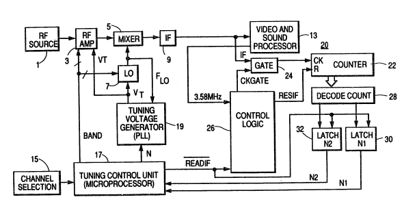
In Figure 1, a source 1 provides a plurality of RF -
television signa}s corresponding to respective channels. An RF
2 () television signal includes modulated picture, color and sound ~ .
carriers. The RF signals supplied by RF source 1 are coupled to an ~ --
RF amplifier 3 which is tuned in response to a tuning voltage (VT)
to select one of the RF signals corresponding to a channel selected ; ~-
by a user. The selected RF signal is coupled to a mixer S. Mixer 5
2 5 also receives a local oscillator (LO) signal generated by a LO 7. LO
7 is also responsive to the tuning voltage to control the frequency
of the LO signal in accordance with the selected channel. Mixer 5 `:,
heterodynes the RF signal selected by RF amplifier 3 with the LO
signal generated by LO 7 to produce an IF signal including
3 0 modulated picture, color and sound carriers corresponding to -
those of the selected RF signal. In the United States the picture
carrier has a nominal frequency of 45.75 MHz, the color carrier `` -.;
has a nominal frequency of 42.17 MHz and the sound carrier has a
nominal frequency of 41.25 MHz. ~ :-
3 5 Rl~ amplifier 3 and local oscillator 7 each include tuned
circuits for de~ermining their frequency responses. Each tuned
circuit includes an inductor and a voltage controlled capacitance
diode, commonly referred to as a "varactor" diode. The varactor
,, . ~
4 ; ~
- - .::
: :
2~7083
RCA 84,268
diode is reverse biased by the tuning voltage to exhibit a
capacitive reactance. The magnitude of the tuni ng voltage
determines the magnitude of the capacitive reactance and
therefore the frequency response of the tuned circuit. Since a .
single varactor controlled tuned circuit configuration is not
capable of being tuned throughout the entire television range,
different tuned circuit configurations are selectively enabled in
response to band selection control signals generated in accordance ;~
with the frequency bands of the selected channels.
] () The IF signal generated by mixer 5 is coupled to an IF
section 9 which filters and amplifies the received IF signal. The -
filtered and amplified IF signal is coupled to a video and sound
processor 13. Processor 13 demodulates the filtered and
amplified IF signal to produce a baseband video signal .~
l S representing luminance, chrominance and synchronizing ~ :`
information. The video information is organized in sequential
fields including line intervals including picture information and
horizontal and vertical retrace blanking intervals including `
synchronization information. Processor 13 also extracts the souncl
2 0 information from the IF signal to produce an audio signal.
The user selects the channel to be received using .
channel selection unit 15 including a keypad (not shown) mounted
on either a remote control transmitter ~not shown) or directly on
the housing of the television receiver itself. A tuning control unit
2 5 17, e.g., comprising a microprocessor operating in accordance with
a stored software program, is responsive to command signals
produced by channel selection unit 15 to generate the band . ~ .
selection control signals for RF amplifier 3 and LO 7 and a digital
signal representing a number N related to the LO frequency for
the selected channel. In the exemplary embodiment, the tuning
voltage (VT) is generated by a phase locked loop (PLL) 19 which
controls the frequency of the LO signal so that it is proportionai to
a reference frequency signal derived from the output signal of a :
crystal oscillator ~not shown) by the number N in the manner
described in greater detail in U.S. patent 4,868,892 issued to Tults, ~.
Testin and Rumreich referred to above. In addition to the channel
number of the selected channel, the number N is also controlled in
response to an AFT signal representing the deviation of the ~ ~ -
2~71~
` RCA 84,268
..
frequency of the IF pi~ture carrier from its nominal value, e.g.,
45.75 MHz in the United States, so as to compensate for any
deviation of the frequency of the RF signal for the selected .
channel from it standard (broadcast) value. The frequency of the ;
S R~ signal may be offset from its standard value when RF source l
comprises a cable distribution network or video accessory, such as
a VCR or video disk player. The manner in which this frequency
correction is accomplished is also described in more detail in the
Tults, et al. U.S. patent.
l O The portion of the tuning system described so far is
conventional. The remaining portion of the tuning system
concerns a digital AFT unit 20 with which the present invention is
primarily concerned.
Digital AFT unit 20 measures the frequency of the IF
picture carrier by counting the number of cycles of the IF picture
carrier during counting intervals or "windows" having a :~;
predetermined duration. The IF picture carrier is amplitude
modulated by picture information during line intervals and other,
mainly synchronizing, information during horizon~al and vertical
2 0 retrace blanking intervals. The picture carrier may be over- - -
modulated with picture information resulting in unreliable
counting of its cycles. Therefore, as earlier noted, it has been
proposed that the cycles of the IF picture carrier be counted only
during the vertical blanking interval (VBI), where the carrier is
2 S not over-modu]ated. However, it may be difficult to determine
when the VBI occurs if the VBI is not of normal form because, e.g.,
the television signal is scrambled, or modified to hamper tape
copying, or weak.
In the present invention, the windows in which
3 0 counting of the IF picture carrier cycles takes place are
distributed throughout a measuring period of at least one field
period of the television signal, e.g., 16.7 milliseconds (ms) in the
United States. Although there is a random phase relationship ~;
between the windows and the VBI, the duration and spacing of . ~-
35 the windows is chosen so that at least one window falls within the
VBI during each measurement period. The counting intervals or
windows are defined by pulses of a stable timing signal. For
example, as is indicated in Figure l, the timing signal may be `~
:' ' '-`' '
^ RCA 84,268
' ~:
derived from the 3.58 MHz color subcarrier osci llator (not shown)
included within video and audio processor 13. By choosing
windows having a duration of 35.76 microseconds (lls) and spaced
by the same amount, the IF picture carrier is sampled about 230 ``
5 times per 16.7 ms measuring period. Therefore, it is assured that
at least some of the windows are within the V13I where the -:
picture carrier is not over-modulated and therefore can be
reliably counted.
The closest frequency tQ the nominal IF picture carrier
I O frequency of 45.75 MHz which has an integral number of cycles - -~
within a 35.76 ~,ls window is 45.751 MHz (i.e., a frequency having
a deviation of 1 KHz). Ideally, e.g., for an IF picture carrier -
frequency of 45.751 MHz and a window of 35.76 lls duration, the ~ :
count per window should be 1636 cycles. However, the phase
relationship of the windows and the IF picture carrier is random, -
so that the count will vary from window to window. This also
applies to other IF picture carrier frequencies. In addition, a ~;,
particular count can be produced for a range of IF picture carrier
frequencies. The probability that a particular count will occur for ~ -
2 0 different IF picture carrier frequencies is indicated by the graph ~`
shown in Figure 2. In the graph, the IF picture carrier frequency
is indicated by the deviation (~IF) from an IF picture carrier
frequency of 45.751 MHz.
The counts produced in the windows spread over the - `.
2 5 field period may be affected by over-modulation of the picture '~
carrier or other causes of dropouts resulting in counts which are
too low (rather than too high). In addition, noise manifests itself -
as signal components having frequencies near the center of the IF
passband, e.g., at about 43 MHz, and therefore results in low
3 0 counts. Consequently, low counts are ignored.
By examining the graph shown in Figure 2, it will be `
appreciated that by detecting only two count conditions, N121636
associated with a range of frequencies surrounding the nominal
picture carrier frequency of 45.751 MHz and N221638 associated
3 5 with the higher adjacent range of frequencies, it can be ;
determined whether the IF picture carrier frequency is low, high,
or within specified limits as indicated in the following table. ln
7 `
2~7~83 ,`
~~-~ RCA 84,268
the table a " 1 " indicates the presence of a count and a "0" indicates
absence of a count. -
. ~ -
TABLE 1
__ __ __ ~ : . :, . . ~, ~
N121636 N2>1638 ~IF(KHZ) IF (MHz)
__ __--'- LOW
O O <-2 8 ~15 ~ 2'
WITHIN LIMITS
1 0 -28~IF<+2 8 45 .7 23 <IF<4 5 . 7 7 9
__ ~ __
~+28 L~_ ~
'~ '.:,'."' '.,": .'
With these underlying principals in mind, digital AFT
20 shown in Figure 1 will be described in detail.
Referring again to Figure 1, an IF signal derived from . ;`
the final IF amplifier of IF section 9 and suitably limited to form a
signal compatible with logic devices is coupled to a gate 24. Gate ,
24 is selectively caused to couple the IF signal to a counter 22 in
response to pulses of a CKGATE signal generated by a control logic ; ~ ~
unit 26 when enabled by the low level of a READIF signal. ~ ~ n.
The low level of the READIFsignal has a duration of 16.7 ms and ~ `
is generated by tuning control unit 17 when it is desired to
measure the IF picture carrier frequency. The CKGATE signal : ~:
defines the counting intervals or "windows" distributed
2 0 throughout the 16.7 ms measuring period.
The cycles of the IF signal passed by gate 24 within
each window are counted by counter 22. Counter 22 responds ~o
the IF picture carrier and not to the other components of the IF
signal because the IF picture carrier is the dominant component of
the IF signal. Counter 22 is reset in response to a RESIF signal ~:
generated by control logic unit 26 immediately before each ~ ~.
window occurs. Selected outputs of the stages of counter 22 ` ~;
which uniquely indicate the presence of the counts N1 and N2 are
coupled to a count decoding logic unit 28 which produces single
3 0 bits indicating the presence ("1"~ or absence ("0") of the respecti~e
-
8 -~ ~
. . .
2 ~ 8 ~
RCA 84,268
counts N1 and N2. The bits indicating the counts N1 and N2 are
stored in latches 30 and 32, respectively. Latches 30 and 32 are
held reset before the beginning of the 16.7 ms measuring period
in response to the high level of the READIF signal, but are not ;
5 reset again during the measurement period.
The contents of latches 30 and 32 are read at the end
of the 16.7 ms measuring period and interpreted according to
Table 1 by tune,r control unit 17 in order to dete:rmine whether
the IF picture carrier frequency is low, high or within specified `~
1 0 limits. Based on the determination, tuning control unit 17 controls ~ -
the number N associated with PLL 19 and thereby the LO
frequency in the manner disclosed in U.S. patent 4,485,404 ~ -
referred to above. Provided the LO frequency is adjusted in steps -~
of less than 56 KHz (the frequency range covered by one
1 5 probability peak indicated in Figure 2) a substantially correct and
stable tuning condition is achievable. For example, the LO
frequency may be adjusted in steps of 31.25 KHz. ~ ~:
An implementation of digital AFT unit 20 is shown in
Figure 3. Waveforms of various signals developed in connection -
with the operation of the implementation of digital AFT unit 20 -~
shown in Figure 3 are illustrated in Figure 4.
As shown in Figure 3, the IF is applied to a NAND gate
comprising gate 24 shown in Figure 1. NAND gate 24 also receives
gating pulses defining the window periods contained with a signal ~ :
designated CKGATE in Figure 3. The gated IF signal, indicated by
the cross-hatched waveform CLKIF, is supplied to the clock input
(CK) of 11-stage ripple counter 22. Counter 22 is reset before the
beginning of each counting interval and is thereafter enabled to
count in response to the signal RSIF.
Count decoding unit 28 comprises a NAND gate 281
having inputs which are coupled to the ones of the outputs
(Q3,6,7,10 and 11) of the counter 22 appropriate for detecting the ` ~ ;
occurrence of a count of 1636 (N1). Decoding unit 28 also
comprises a NOR gate 282 having inputs coupled to the Q2 output
3 5 of counter 22 via an inverter 283 and to the output of NAND gate
281 for detecting the occurrence of a count of 1638 (N2).
The "set" input of latch 30 (comprising two NOR gates ,~
in a cross-coupled configuration to form a flip-flop or bistable
:- ~ ;, .
- ~ '.:,-::
~~ RCA 84,268 2 0 3 7 0 8 3
multivibrator) is coupled to the output of NAND gate 281 via an
inverter 284. The set input of latch 32 (also comprising two
cross-coupled NOR gates) is coupled to the output of NOR gate 282. ~ ~ ,
Latches 30 and 32 are held reset to logic "0" by the READIF
:- signal when this signal is high. The outputs of latches 30 and 32
are set to log;cal 'l's upon the occurrence of the counts N1 and N2,
respectively The outputs of latches 30 and 32 are coupled to
tuning control unit 17. ;~
Control logic unit 26 comprises an 8 stage ripple
I O counter 261 which counts the cycles of a 3.58 MHz crystal
oscillator 262 to produce various control signals shown in Figure
4. As indicated in Figure 1, crystal oscillator 262 may comprise
the color subcarrier oscillator (not shown) of the receiver
contained in video and sound processing unit 13.
1 5 The control signals are produced when counter 261 is enabled in
response to the low level of the READIF' signal applied to its reset
(R). The READIF signal also enables a latch 263 comprising four
NAND gates, and an inverter. Latch 263 receives the Q8 output
(also identified as WNDW ) and the Q4 output of counter 261. As . .-~
shown in Figure 4, the state of the outputs of latch 263
(DELWNDW and DELWNDW ) change after the state of WNDW
(Q8) changes in response to the next leading edge of the Q4 pulse
(provided READI:F is low). The CKGATE signal for allowing the IF ~ -
signal to reach the clock (CK) input of counter 22 is produced by a -
2S NAND gate 264 in response to the WNDW (Q8) and DELWNDW
signals. The RESIF signal for resetting counter 22 at the beginning
of each counting window is produced by a NOR gate 265 in
response to the DELWNDW and WNDW signals.
Tuning control unit 17 shown in Figure 1 reads the
30 contents of latches 30 and 32 just before the positive transition of
READIF signal after the 35.76 ,us wide counting windows
separated by 35.76 ~lS have been generated for a time period of at
Ieast 16.7 ms as indicated in Figure 4. After reading N1 and N2,
tuning control unit 17 will act as follows~
;
. ~, .
1 0 ; '
~.~
RCA 84,268
1. If Nl=1 and N2=1, then the IF ~ - -
frequency is too high and the LO
frequency is decreased, e.g. by 31.25 -
KH~. ~ ~'''''
2. If N1=1 and N2=0, then the IF
frequency is within specified limits and
the LO ~requency is left unchanged.
3. IF N1=0 and N2=0, then the IF -
frequency is too low and the LO
frequency is increased, e.g., by 3 1 .25
Another implementation of a digital AFT unit is sllown
in Figure 5. Waveforms for various signals developed in
connection with the implementation shown in Figwre 5 are shown
15 in Figure 6.
The major difference between the digital AFI' unit shown in
block diagram in Figure 1 and in more detail logic diagram form in ~ :
Figure 3 and the AFT unit shown in Figure 5 is that the functions
performed by count decoder 28 and latches 30 and 32 of the `~
20 digital AFT unit shown in Figures 1 and 3 are performed by
tuning control unit 17 under software program control in the
digital AFT unit shown in Figure 5. To accomplish this, the ` ~`
contents of counter 22 are coupled to bus interface unit 23,
including a parallel-to-serial converter, which converts the bits
2 5 representing the count to a serial bit stream which is coupled to
tuning control unit 17 via a serial data bus 25. The contents of ;
counter 22 are partially decoded by a logic arrangement including
NAND gate 288 and NOR gate 289 to produce a signal indicative of
a count of 1536 so that only the Q2-Q8 outputs of counter 22 and ;
3 0 the 1536 count indication, consisting of a total of 8 bits compared
to the 12 output bits of counter 22, need to be coupled to tuning
control unit 17. By way of example, serial data bus 25 may be of
the type employed in television receivers manufactured by
Thomson Consumer Electronics of France and illustrated in Figures
3 5 5 and 6. Serial data bus 25 may also be of the well known IM
(INTLRMETALL) type developed by ITT INTERMETALL
Semiconductors of Germany described in the ITT publication "Digit
2000 VLSI Digital TV System" or of the also well known I~C (Inter
.
2 ~ 3 7 ~ g 3 ~
~~ RCA 84,268 ;~
IC) type developed by Philips of The Netherlands and described in
Philips Technical Publication 110 - "I2C Bus In Consumer
Electronics".
Briefly, as is indicated in Figure S, serial bus 25
5 includes three conductors: one for a DATA signal; one for a CLOCK
signal; and one for an ENABLE signal. The waveforms for these
three signals are illustrated in Figure 6. Data bus 25 is "bi-
directional", i.e., data can be coupled in both directions between a
"master" unit, usually including a microprocessor such as tuning
10 control unit 17, and a "slave" unit including a bus interface unit
such as bus interface unit 23. The data is synchronously
transmitted with respect to clock pulses of the CLOCK signal. The
CLOCK signal is generated by tuning control unit 17 and is used by
bus interface unit 23 to decode the DATA signal. The ENABLE
15 signal is also generated by tuning control unit 17 and initiates the
communication process between tuning control unit 17 and bus
interface unit 23.
A first, i.e., low level, portion of the ENABLE signal is
used to transmit or "write" data from the master unit to the slave
2 0 unit. During a first interval of the "write" portion, an "address"
word, e.g., of 8 bits, indicating the function to be controlled is
transmitted. During a second interval of the "write" portion, a
data word, e.g.,of 8 bits, representing a particular aspect of the
function to be controlled may be transmitted. In the digital AFT
25 unit shown in Figure 5, the "address" word is used to transmit a
READIF command for causing bus interface unit 23 to generate the
low level of the READIF signal as indicated in Figure 6. A second, ~;
i.e., high level, portion of the ENABLE signal is used to transmit or
"read" data from ~he slave unit to the master unit. Two data ~ -
3 0 words, e.g., of 8 bits each, may be transmitted during the "read"
portion of the ENABLE signal. The first data word must include a ~ ~
confirmation of the receipt of the "address" word transmitted ;;~
from the master unit and may comprise a portion of the "acldress"
word. In the digital AFT unit shown in Figure 5, the second data
3 5 word is used to transmit the data representing the count of
counter 22 (i.e., Q2 - Q8 and the "1536" count indication bit) to
tuning control unit 17.
1 2 ~ -
2 ~ 3 7 ~ g ~
~` RCA 84,268
The flowchart for the portion for the program
associated with the digital AFT unit shown in Figure 5 is shown in -
Figure 7. As indicated in Figure 7, after the AFT subroutine is -~
initiated, a "timer" for measuring elapsed time is started and the
READIF command is caused to be transmitted. The resulting low
level of the READlF signal enables control logic unit 26 to
generate the CKGATE signal which establishes a 35.76 ~s counting -
window. In the implementation shown in Figure 5, control logic
unit 26 includes a 7-stage ripple counter 266, a NAND gate 267, a ; ~;
l 0 2-stage ripple counter 268 and an inverter 269. The waveforms :
for a Q7 CLK signal and a Q7 GATE signal generated within control
logic unit 26 are shown in Figure 6. The high level of the CKGATE ~ -
enables a NAND gate, serving as gate 24, to couple the IF signal to
counter 22 as is indicated by the cross-hatched portion of the
I S signal CLKIF.
After the termination of the 35.76 lls counting
window, i.e., when the CKGATE signal returns to the low level, ;
tuning control unit 17, under software control, examines contents
of counter 22 to determine whether the count represented by the
2 0 11 bits is equal to or larger than 1636 or 1638 and memorizes the
result. The examination can take place any time after 53.66 lls
(17.9 ~s + 35.76 lls) has elapsed after the negative transition of
the READIF signal as indicated in Figure 6. This time is "known"
by tuning control unit 17 since clock pulses of the CI,OCK signal,
2 5 which synchronize the communication between tuning control unit '
17 and the digital AFT unit are generated by tuning control unit
17 and are therefore related to its instruction cycles. As indicated
in Figure 7, this sequence is repeated over a time period of at
least 16.7 ms. Since the communication between tuning control
3 0 unit 17 and bus interface unit 23 requires slightly more 256 ,us -~
(i.e., 4 words x 8 bits/word x 8 !ls/bit) and the VBI includes at
least 9 lines having a total duration of 571.5 lls (9 lines x 63.5 ~s),
it is possible to ensure that at least one counting interval occurs
during the VBI if the process is repeated, e.g., every 500 ~lS.
3 5 At the end of 16.7 ms measurement period, if one or ~ ~ `
more of the count samples o~tained during the 16.7 ms '~
measurement period was 1638 or greater, then the LO frequency
is decreased by decreasing N. If none of the count samples was
1 3
~: RCA 84,268 2037083 ~ ~ :
equal to or greater than 1636 then the LO frequency is incre~sed.
If one or more of the count samples was equal to or greater than
1636 but none was equal or greater than 1638, the LO frequency
is left unchanged. .
It is noted, for comparison, that in the implementation
shown in Figure 5, the low level of the READIF determines the ~ .-
duration of one measurement interval within the 16.7 ms
measurement period. However, in the implementation shown in
Figure 3, the low level of the READIF signal corresponds to the
entire 1 6.7 ms measurement period.
Compared to the implementation shown in Figure 3,
the logic circuitry of the implementation shown in Figure S is less
complex. However, this is achieved at the expense of a somewhat
more complicated software program required for evaluating the ~ .
I 5 counts.
Preferably, the digital AFT unit shown in Figure 5 is -
incorporated in an integrated circuit with other portions of the
television receiver such as IF section 9 and sections of video and
sound processing unit 13. In that case, data bus 25
2 0 advantageously both serves to control the various functions of the
integrated circuit as well as to control the digital AFT unit and to
receive IF picture carrier frequency deviation information from it.
It will be understood that the present invention has
been described with reference to a preferred embodiment by way
of example and that modifications will occur to those skilled in the ;~
art.
For example, although a phase locked loop (PLL) is
employed in the embodiment shown in Figure 1 to generate the
tuning voltage, a frequency locked loop (FLL), such as disclosed in -~
U.S. patent 4,485,404 issued to Tults referred to above, may also
be employed. For that matter, an opened loop voltage synthesis
arrangement utilizing a digital-to-analog converter for converting
a digital word to a DC level may be employed.
In addition, the frequency of the IF signal may be -~
3 5 divided by a frequency divider (known as a "prescaler") before
being coupled to the digital AFT unit.
Further, while the IF signal coupled to digital AFT unit ` --~
20 was said to be derived from the final IF amplifier of IF section
1 4 ;
RCA 84,268 2 a ~ 7 ~ 8 3
9, it may be derived in other ways. For example, the IF signal
may be derived from the tuned circuit (not shown) of the
synchronous video detector (not shown) included with video and
"udio signal processing section 13. Advantageously, the pulse
signal produced at this point due to the limiting devices (e.g., ~;
diodes) may be compatible with the logic devices of the digital
AFT unit 20.
Still further, while it was indicated with reference to
the software program depicted in Figure 7 that the actual count
I 0 after each counting cycle is stored, it is also possible to sto~e only
indications that the counts N1 and N2 ~,vere produced. In that
case, after the 16.7 ms measurement period has elapsed, it is only
necessary to determine which ones, if any, of the N1 and N2 count
indications have been stored. Furthermore, with respect to the
15 software program indicated in Figure 7, it is possible to terminate
the routine once both of the counts N1 and N2 have been
produced and immediately proceed to the desired LO frequency
adjustment.
Even further, portions of the digital AFT unit, such as
. 2 0 counter 22, may be de-energized at times other than during the
measurement period in order to save energy. In that case, a delay
should be provided between the beginning of the measurement
period (corresponding to the negative transition of the READIF
signal) and the beginning of the counting interval (corresponding
25 to the positive transition of the CKGATE signal) to allow sufficient
time for the de-energized portions of the digital AFT unit to be
energized. The 17.9 lls delay of the CKGATE signal illustrated in
Figure 6 has that purpose. ; ~ ~
These and other modifications are intended to be ..
3 0 within the scope of the invention defined by the following claims.
3 5
,",^~': '