Note: Descriptions are shown in the official language in which they were submitted.
2057123
65259-138
The present invention relates to a semiconductor
device and, more particularly, to an electrode structure of a
semiconductor device and a method of making it. In the specifica-
tion of this application, plane orientations are denoted by sym-
bols, such as (001) and (111), but these symbols also denote
equivalent planes, because of crystallographic symmetry. Further,
zone axes are denoted by symbols, such as [011] and [011]. These
symbols also denote equivalent zone axes, because of the
crystallographic symmetry.
BRIEF DESCRIPTION OF THE DRAWINGS
Figure 1 is a plan view of a portion of a conventional
semiconductor device;
Figure 2 is a cross-sectional view along the line 2-2
of the device shown in Figure l;
Figure 3 is a plan view of a portion of a semiconduc-
tor device according to one embodiment of the present invention;
and
Figure 4 is a cross-sectional view along the line 3-3
of the semiconductor device shown in Figure 3.
BACKGROUND OF THE INVENTION
Some prior art semiconductor devices employ an
electrode structure, such as shown in Figures 1 and 2. The semi-
conductor device shown in Fig~res 1 and 2 includes a semiconductor
layer 11 of a III-V compound semiconductor, such as GaAs and InP.
A semiconductor layer 12 is disposed on a major surface of the
semiconductor layer 11. The plane orientation of the major
- 1 -
2057123
65259-138
surface is (100). The semiconductor layer 12 is also of a III-V
compound semiconductor, such as GaAs and InP and has an edge
portion extending straight along the [010] direction, as shown in
Figure 2. The orientation of the plane of the side surface 14 of
the edge portion is (001) which is orthogonal to the major surface
of the semiconductor layer 11. The semiconductor layer 12 is
formed by epitaxially growing a semiconductor layer over the entire
major surface of the semiconductor layer 11 and, using a mask,
etching away undesired portions of the epitaxially grown semi-
conductor layer until the portions of the major surface of the
layer 11 beneath them are revealed. A conductor electrode 13 is
disposed to lie over both of the major surfaces of the semiconduc-
tor layers 12 and 11. The conductor electrode 13 is formed by
vacuum vapor depositing a metal onto the major surfaces of the
semiconductor layers 11 and 12 from the direction perpendicular
thereto, so that the conductor electrode 13 has a step presenting
a side surface 16 near the side surface 14 of the semiconductor
layer 12, as shown in Figure 2.
Because the conductor electrode 13 is formed by vacuum
vapor deposition in the direction perpendicular to the major
surfaces of the semiconductor layers 11 and 12, the distance ts
of the side surface 16 of the conductor electrode 13 from the
extension of the side surface 14 of the semiconductor layer 12 is
substantially smaller than the thickness to f that portion of the
conductor electrode 13 which lies on the major surface of the
semiconductor layer 12. In an extreme situation, the distance
2057123
65259-138
ts may be zero and, therefore, the conductor electrode 13 may be
disconnected. One may contemplate to use a sputtering technique,
instead of vacuum vapor deposition, trying to form the conductor
electrode 13 with a larger ts, since, in sputtering, the mean free
path of film forming particles is small and, accordingly, a
relatively large number of the film forming particles tend to turn
around. However, such film forming particles still impinge
perpendicularly to the major surface of the semiconductor layers
11 and 12, and, therefore, the distance ts is only 10-20 % of the
thickness to. Furthermore, due to some etching conditions, a poor
adhesion of an etching mask used to form the semiconductor layer
2, etc., the orientation of the side surface 14 may sometimes be
displaced from its desired (001) orientation so that the ratio
ts/to may vary considerably depending on etching conditions. If
the distance ts is small, when current I is applied to the con-
ductor electrode 13, the resistance value of the electrode 13 at
the portion with the thickness ts becomes large and, accordingly,
the Joule heat Q generated at that portion, which is expressed as
Q = I2R, becomes large. Ultimately, the temperature at the por-
tion may reach the melting point of the material of the conductor
electrode 13, so that the electrode 13 melts and is disconnected.
An object of the present invention is to provide a
semiconductor device with a large value of the distance ts to
avoid disconnection thereof, and also a method of making such a
semiconductor device.
In order to achieve the above-identified object, the
2057123
65259-138
semiconductor device according to the present invention comprises
a layer of a III-V compound semiconductor material having a major
surface in the (100) orientation, which has a side surface formed
by etching the major surface. The semiconductor device also
includes an electrode disposed on said semiconductor layer in such
a manner as to pass over said side surface. The side surface of
the semiconductor layer beneath the electrode includes at least
one region in the [011] orientation, and this region is in the
(111) orientation.
A method of making a semiconductor device of the
above-described type includes a step of etching a III-V compound
semiconductor layer from its (100) oriented major surface with
a mask including at least one region in the [011] orientation to
thereby form a step in the semiconductor layer, and a step of
depositing an electrode material on the semiconductor layer from
the direction perpendicular to the major surface thereof to there-
by form an electrode which overpasses the step in the seml-
conductor layer.
DETAILED DESCRIPTION OF THE INVENTION
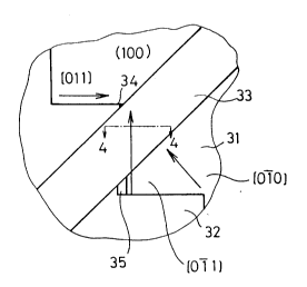
Figures 3 and 4 shows a semiconductor device according
to one embodiment of the present invention. The semiconductor
device includes semiconductor layers 31 and ~2. Although the
details are not shown, the semiconductor layer 31 comprises a
plurality of semiconductor layers, which are layers of a III-V
compound semiconductor material, such as GaAs InP and AlGaAs,
layers of
- 3a -
2057123
65259-138
the semiconductor with a donor or an acceptor added The
semiconductor layers 31 and 32 form, for example, a semiconductor
laser. The upper or major surface of the semiconductor layer 31
is in the (100) plane.
The semiconductor layer 32 is disposed on the semiconductor
layer 31, and it also comprises a III-V compound semiconductor
material, such as GaAs, InP and AlGaAs, or such a semiconductor
material with a donor or an acceptor added thereto. The upper
or major surface of the layer 32 is also in the (100) plane. The
semiconductor layer 32 is formed by means of epitaxial growth and
etching techniques. As shown in Figure 3, the semiconductor layer
32 has a step which extends generally in the direction along the
[010] orientation. The step includes a region 34 extending in
the direction along the [011] orientation, and a region 35 which
connects the region 14 and extends in a direction perpendicular
to the region 34 along the [011] orientation. The surface of the
region 35 is in the (111) plane, as shown in Figure 4. In other
words, the region 35 tapers downward toward the major surface of
the semiconductor layer 31.
On the upper surfaces of the semiconductor layers 31 and 32,
a conductor electrode 33 is disposed to overpass the region 35
to connect the layers 31 and 32. For example, Al may be used as
a material for the electrode 33. A vacuum vapor deposition
technique may be used to form the conductor electrode 33. The
thickness ts of the portion of the electrode 33 which overlies
the region 35 is as large as about 58 % of the thickness to of
the portion which overlies the second semiconductor layer 32.
The semiconductor device with the above-described structure
may be made in the following manner. First, the semiconductor
layer 31 is prepared by a conventional technique Then, a
semiconductor layer, from which the second semiconductor layer
32 is to be formed, is epitaxially gro~n on the entire major
surface of the semiconductor layer 31. The upper or major surface
of the epitaxially grown semiconductor layer is in the (100) plane
This layer is etched to provide the semiconductor layer 32 A
wet etching technique may be used, in which, for example, a mixture
205712~
solution consisting of sulfuric acid, hydrogen peroxide and water
may be used as an etchant. Before performing etching, a mask is
disposed on the upper surface of the epitaxially grown
semiconductor layer. The mask has an opening therein which is
defined at least by edges corresponding to the edges of the step
regions 34 and 35 shown in Figure 3. When the above-described
etchant is used to etch a III-V compound semiconductor, V atoms
having unpaired electrons are active to reacting molecules of the
etchant and, accordingly, react rapidly, whereas III atoms having
no llnpAired electrons are slow in reaction. For example, As, which
is a V element, reacts fast with hydrogen peroxide in the etchant
and turns into arsenic oxide which is dissolved in sulfuric acid
In contrast, Ga, a III element, reacts slowly with hydrogen
peroxide and hardly turns to gallium oxide. Accordingly, the
amount of gallium dissolved into sulfuric acid is small and a
quantity of gallium remains on a surface being etched. When the
(100) plane major surface of the III-V compound semiconductor layer
is etched with the above-described etchant, a region extending
in the [011] direction, e.g. the region 35, will have its (111)
plane surface revealed. As the (111) plane has a slope of 54.7'
with respect to the (100) plane, the region 35 has its surface
slanting downward toward the major surface of the semiconductor
layer 31 at an angle of 54.7 .
After the etching step, a suitable material is deposited onto
the major surfaces of the layers 31 and 32 from above them through
an appropriate mask to dispose the electrode 33. The electrode
material is deposited in a direction substantially perpendicular
to the major surfaces of the layers 31 and 32. For example, vacuum
vapor deposition may be used for forming the electrode 33. The
thickness ts f the portion of the thus formed electrode 33 which
overlies the surface of the region 35 has been calculated from
the slope of the surface of the region 35 relative to the major
surface of the semiconductor layer 31, and it has been known to
be as large as about 58 % of the thickness to of the portion which
overlies the major surface of the semiconductor layer 32.
In the above-described embodiment, the semiconductor layer
2057123
65259-138
32 disposed on the semiconductor layer 31 is etched, and the
electrode 33 is disposed on the layers 31 and 32. However, the
major surface of the layer 31, with no semiconductor layer disposed
thereon, may be etched and the electrode 33 can be disposed
thereon. Furthermore, dry etching may be employed in instead of
wet etching.
As described in detail in the above, according to the present
invention the ratio tS/to of the electrode 33 can be made
considerably larger than ones which could be provided by conven-
tional techniques. Furthermore, because the orientation of the
surfaces to be etched is relatively stable, a large value of ts
can be obtained with high reproducibility. Thus, probability of
disconnection of conductor electrodes can be almost completely
avoided and, accordin~ly, high reliability can be achieved.