Note: Descriptions are shown in the official language in which they were submitted.
BACXGROUND OF THE INVENTION
Fle~_g~the Inventlon
The lnventlon relates to data proce~slng systems and, more
partlcularly, to data processing sy~tems employing multiple buse~.
Discusqion of the Related Art
In computers and data processing system~, a bus i~ commonly
employed to interconnect the various elements of the ~ystem. ~or
example, a central processing unit is typically connected tO
memory components, input/output (I~O) devices, etc., via a bus
capable of carrying the -Rignals associated with the operation of
each element. The~e signals include, for ex~mple, data signalq,
clock signal~, and control 3ignals. The bus must be capable of
carrying such signals to all components coupled to the bus so that
the de~Lred operation can be carried out by the computer system.
As computer system~ achieve increasingly hlgher levels of
performance, it is sometimes de~irable to provide more than one
bus in the computer system. For example, it may be desirable to
provide a high speed main systam bus which Lnterconnects
processors ~nd hlgh speed memory component9, and to provide a
separate bu~ whlch lnterconnects I/O devlce~ such as di~k drives
and tape drive~ to an I/O controller.
Inltially, m~nufacturers of computer systems provided
proprletary bu~e~ with which to interconnect componants of the
qystem. There i8 now an incre~ing trend toward the use of
stand~rdized buse~, in which specification~ of the bu~ are
publi~hed for use by all manufacturers. Many manufacturers an
then ~upply components specific~lly for ug~ with the standA-i ~us.
, ..
2 & ~ ~ 1 ri ~
Multiple standard buse~ are now available, each having a
dlffarent set of characteristics. However, there iQ an increasing
need to provide the capability to assemble computer systems
employlng components connected to various types of ~tandard buses.
Method~ and apparatus for providing such interconnections are
known in the art. Rnown interconnection systems employ serial
lines, ribbon cable, and fiber optics. For example, methods and
apparatus for interconnecting computer buses u~ing an
interconnection known as the I3US are described in U.S. Patent
4,858,234 issued August 15, 1989 to David W. Hartwell et al., and
assigned to the a~ignee of the present invention.
As a result of such trends, the importance of variou
features of an interconnection system is becoming apparent. For
example, it is de~irable for an interconnection qystem to provide
high data tran~fer rate3 between buses, such that functionality on
high performance buse~ i9 not compromised due to waiting time
cau~ed by an ineff$cient bus interconnection ~ystem. It is
further desirable to provide methods and apparatus for
interconnectlng information buses of different sizes and to
provide $nterconnection between different cabinets, without
requlrlng a backplane connection between buses. Intercabinet
conn-ctivlty g~ve~ ri3e to the need for high no$se immunity and,
corre~pondingly, low noi~e emissionq. It i~ further de~irabla to
provide methods and apparatus for interconnecting buses which
utilize the minimum nu~ber of interconnection lines.
With the increasing num~er of standardized buses, it is
important for a manufacturer to enable interconnectivity of ~he
--2--
2 U 3 7 ~
manufacturer's product3 with as wide a variety of standard bus
sy~t~ a~ pos~ible. Implementation of cu~tom interconnection
method- and apparatus for each bus pair gives rl~e to hlgh design
and manufacturlng cost. It i9 therefore desirable to provide
apparatus and methods for interconnecting information buqes which
are extremely flexible, and employ a larqe number of common
component~ to-permit multiple interconnection applicationq with a
minlmum of co~t.
None of the ~nown methods and app~ratu~ for interconnecting
inform~tion bu~es fully meet the requirements noted above.
SUMMARY OF THE INVENTION
It is an ob~ect of the present invention to provide methods
and apparatus for connectlng information buses which more fully
meet the requirements noted above than currently known methods and
apparatu~. Additional ob~ects and advantages of the invention
will be set forth in part in the descrlption which follows and, in
part, will be obvlou~ from the description or may be learned by
practice of the lnvention. The ob~ects and advantaqe~ of the
invention wlll ba re~lized and attained by means of the
instrumantalitle4 and combination~ particulaxly pointed out in tha
appond~d clalm~.
To achlevs the obJect~ and in accordance with the purpose ef
tha inventlon, a~ embodied and broadly de~cribed herein, the
invention, ln one aRpect, compri~es apparatu~ for interconnec~ ng
fir~t and second information bu~es each having a plurality oF ~ata
linas. T~e apparatu~ includes fir~t and ~econd multiconduct~-
unidirectionsl information paths each having a plurality o~ a
2 0 ~ 7 1 ~ ~3
sign~lJ, the number of data ~ignals in each information path being
le~ than the number of data lines in at least one of the
inform~tion buses. The apparatus further includes a first
interconnect module comprising a first pair of regi~ters each for
respectively receiving a set of a first pair of setQ of
informatlon appearing on a first pair of sets of data lines of the
first information bus, a first multiplexer for sequentially
tran~ferring e~ch set of the first pair of set~ of inform~tion
from the fir~t pair of regi~ters over the data lines of the first
information path, ~nd a first connector coupled to the first
multiplexer.
The apperatus additionally includes a second lnterconnect
module comprising ~ second pair of registers each for respectively
supplying a 3et of the first pair of sets of information to a set
of a second pair of ~et~ of data lines of the second information
bus, a econd connector removably connected to the first
connector, and a flrst demultiplexer coupled to the second
connector for receiving the first pair of sets of information
sequentially tran4ferred by the multiplexer and for respectively
supplying the first pair of sets of information to the second pair
of r-gl~ter~. Further, the apparatus include~ a third
lnt~rconnect module compri~ing a third pair of registers each for
re~pectively recelving a set of a second pair of sets of
lnformation appearing on the second pair of set~ of data lines of
the s~cond information bus, a second multiplexer coupled tO the
second connector for ~equentially transferring each set of he
second pair of set~ of information from the third pair of
--4--
~ O ~
regl8ter~ over the data lines of the second lnformation path; and
~ fourth interconnect module comprising a fourth pair of regi~ters
each for respectively supplying a set of the second pair of sets
of information to a set of the first pair of sets of data lines of
the fir~t inform~tion bus, and a second demultiplexer coupled to
the flrst connector for receiving the second pair of sets of
information sequentially transferred by the second multiplexer and
for re~pectively ~upplying the second pair of sets of information
to ~he fourth pair of registers.
The inventlon, in another a~pect, comprises a method for
interconnecting fir~t and second information buse~, each having a
plurality of d~ta lines, over first and qecond multiconductor
unidirectional information paths e~ch having a plurality of data
signals, the number of data signals in each information path being
leqs than the number of data lines in at least one of the
information buses. The method include~ the ~tep~ of respectively
receiving a fir~t pair of sets of information from a first p~ir of
set~ of data line~ of tho fir~t information bus into a first pair
of regi~ter~; oper~ting a first multiplexer to sequentially
transfer each set of the first pair of sets of information from
the flr~t p~lr of register3 over the data lines of the first
infor~atlon path; respectively receiving, in a 3econd pair of
regi0ters, the first pair of sets of information sequentially
tranqferrad by the first multiplexer; raspectively and
simultaneously supplying the fir~t pair of sets of information
from the econd palr of registers to a second pair of sets of 8dt~
lines of the second informatlon bus; respectively receivin~
--5--
~ ~ _ _ 1 r; ~
second palr of sets of information from the second pair of ~ets of
data linea of the second information bus into a third pair of
reqisters; operating a se~ond multiplexer to sequentially transfer
each set of the second pair of sets of information from the third
pair of registers over the data lines of the second information
path; respectively receiving, in a fourth pair of registers, the
second pair of sets of information sequentially transferred by the
second multiplexer; and respectively and simultaneously supplying
the second pair of sets of information from the fourth pair of
register~ to the first pair of sets of data lines of the first
informatlon bus.
The accompanying drawings which are incorporated in and
constitute a part of the specification, illustr~te one embodiment
of the lnvention and, together with a description, serve to
explain the principals of the invention.
RIEF DESCRIPTION OF THE DRAWINGS
Figure 1 i3 a block diagram of a computer system comprisinq a
pair of inform~tion buses each having a plurality of componene~
and connected by an interconnection system includinq a pair of
adapters and an interconnection bu~, according to a preferred
embod~ent of the prssent invention
Flgure 2 i~ a block diagram of the bus adapters and
$ntorconnection buR of the system of Figure l;
Plgure 3 is a detailed block diagram of an interface circult
of the first adapter of Figures 1 and 2;
Figure 4 iY a detailed block diagram of an intarface c.rcu e
of the second adapter, shown in Figures 1 and 2;
2 Q 3 r~ ~ ~! J
Flgure 5 i8 a block dlagram of an interconnect transmitter
includ~d ln the adapters of Figures 3 and 4;
Flgure 6 i~ a block diagram of an interconnect receiver
included ln the adapters of Figures 3 and 4;
FigUrQ 7 i9 an electrical schematic diagram ~howing
termination circuitry for the transmitters and receiver~ of
Figures 5 and 6, respectively;
Figure 8 is a timing diagram showing timing relationships
between signals of the system shown in Figures 1-6;
Figure 9 i9 a detailed block diagram showing the
configuration of the control circuit of Figure 4~
Figure 10 i~ a detailed block diagram showing the
configurat$on of the control circuit of ~igure 5; and
Flgure 11 is a detailed block diagram of control circuits of
Figuros 5 and 6.
DETAILED DES~RIP~IQh OF THE PREFERRED EMBODIMENT
Refer~nce will now be made in detail to the pre~ently
preferred embodiment of the invention, an example of which is
illu~trated in the accompanying drswings. Throughout the
drawing~, llke reference character~ are used to indicate like
el~ont~.
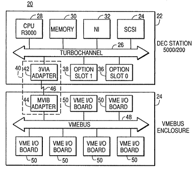
~ igure 1 show~ an examplo of a data proce~sing sy~tem 20
which embodies the present invention. System 20 include~ fi-
~and socond sub~ystems 22 and 24. Subsystem 22, in the preferred
Qmbodiment, compris6s a DECstation 5000/200 engineering
workQt~t~on manufactured by the Digital Equipment Corporation.
Sub y~te~ 22 includes a plurality of component~ interconnected by
2~ 71 7~
a system bus 26 which, in the preferred embodiment, comprises d
st~ndard thlrty-two bit public buq known ac the TURBOchannel, and
which ~echanically includes a cabinet having multiple slots
interconnected by backplane wiring. The thirty-two bit
designation refers to thirty-two signal lines of the TURBOchannel
which carry address and data information at various times. Such
lines will henceforth be referred to as data lines , as
distinguished from control lines which carry types of information
other th~n addre~ an~ data information.
The TURBOchannel i~ an internal system bu~ used in products
manufactured by the Digital Equipment Corporation, the assignee of
the pre~ent invèntion. The TURBOchannel constitutes an open
architecture~ bu3, and detailed specifications of the TURBOchannel
are de~cribed in the TU~BOchannel hardware specification, Order
No. EK-369AA-OD-005, publicly available from the DLgital Equipment
Corporation. Subsystem 22 includes a ~y~tem module 28 connected
to system bus 26. In a preferred embodiment, ~ystem module 28
comprise~ a R300C proce~sor.
Sub~stem 22 also include~ a plurality of option modules.
Such option modules may include a memory 30, a communications
~ethorn~t) controller 32 (designated NI in Flgure l), and a Small
Co~ut-~ System Interface (SCSI) controller 34. Sub~ystem 22 also
include~ a pair of slots 36 and 38 which may receive other sys;em
componehts such a~ additional memory or controllers.
Sy~tem 20 also includes an interconnection apparatus ~0 which
in turn comprises first and second adapter modules 42 and ~
interconnected by an interconnection bus 46. Adapter modu'e ~2 i9
2~171
removably connected to system bus 26 by occupying a qlot in the
TURBOchannel cabinet.
In the preferred embodiment, second subqy~tem 24 comprises a
VMEbus syqtem including a second system bus 48. System buq 48, in
the preferred embodiment, constitutes a VMEbuq, which is an
asynchronou~ interlocked bu~ with separate data and address lines.
The VMEbus iq an indu~try-standard bus defined by IEEE Standard
1014. Sub~y~tem 24 further include~ a plurality of VME I/O boards
50, commercially available from a number of ~ources including
Motorola Corporation and performing such functions as array
proce~qlng, image proce-~sing, communications control, and I/O
operation~. Second adapter module 44 i~ romovably connected to
second system bu~ 48, by occupying a slot on bus 48.
Although the pre~ent invention provides the capability for
interconnecting a wids variety of buse~, sub~ystem 22 in the
preferred embodiment constitute~ a host subqystem and subsystem 24
constitute4 an I/O ~ubsystem. First syRtem bus 2S will be
referred to as ~the ~URBOchannel~ (or "3MAX") and -~ystem bus 48
will b6 referred to a~ ~the VMEbus.~ Adapter 42 will be referred
to a~ ho~t adapter 42. Host adapter 42 will also occasionally be
referr~d to in table~ a~ ~3VIA.~ Similarly adapter 44 will be
referr-d to as I~O adapter 44 or, in tableq, a~ "MVIB."
Interconn~ction bu~ 46 will be referred to in tables as ~YAbus.~
Referring now to Figure 2, interconnect apparatus 40 is shown
in greater detsil. Interconnection bus 46 of apparatu~ 40
in~ludes first and qecond multiconductor unidirectional
information path~ 52 and 54 each having a plurality of data
2 ~ J ~
slgnal-, the number of data 3ignal5 in each information path beins
le~ than the number of data lines in the TUR90channe! 26 and th2
VMEbu~ 48. In the preferred embodiment, information paths 52 and
54 each lnclude slxteen data signals. In particular, lnformation
path 52 inc~ude~ fir~t and second twisted-pair cable~ 56 and 58
each comprlsing a plurality of twisted-pair conductors and
respectively connected to first and second connectors 60 and 52.
Path 54 include~ third and fourth twisted-pair cables 64 and 56
re~pectively connected to connector~ 62 and 60. In addition,
information paths 52 and 54 each include three parity signals,
three typQ-and-mas~ signals, a strobe signal, and a re3et si~nal.
Information paths 52 and 54 thu~ include forty-seven pairs of
twisted conductors (plus three spares) enclo~ed in both braid and
foil shields. Pin numbers of information paths 52 and 54, ln
preferred embodim~nt, arQ shown in Table l.
TA~
P~
_
v~
2 C~u~vU~ r~
c~u ~ v~ s~ ~ ,r~
c~u ~ v~ r~
C~U ~ V~
C~
" V~ ~ C~U ~"~1
2 vu~C~U r~
V~ ~ C~U S~ ~ ~A~
V~ ~ C~U S~ 1
t vut~C~u Sr~
.
-10--
2~7~
Each ~lgnal requires two pin~ with twisted-pair wiring.
Although the present preferred embodiment employs a unieary cable
includlng fifty pairs of twisted conductors surrounded by shields
and interconnected by first and second connectors 60 and 62, the
invention i~ not so limited. Other types of connections could, of
course, be employed, as i9 readily under~tood by those skilled in
the art.
~ pparatu~ 40 also includes first, 3econd, third, and fourth
interconnect modules 68, 70, ?2, and 74. Modules 68 and 72 are
identlcal and each constitute an interconnect transmitter.
Modules 70 and 74 are identical and each conetitute an
interconnect receiver. Thus, only modules 68 and 70 will be
described in detail. Host adapter 42 includes a host interface
circuit 75 and adapter 44 includes an I~O interface circuit 76.
~ ccording to the preferred embodiment, host interface
circuit 75 i~ specifically adapted to interface with a first
inform~tion bu~, ~uch ~ TURBOchannel 26. I/O interface
circult 76 is specifically adapted to interface with a second
infor~ation bu~, such as VMEbus 48. A~ will be de~cribed below in
gre~te~ detail, hoRt interface circuit 75 receives and transmi-s
over TU*~Ochannel 26 u~ing in~tructions defined as p~rt of t~.e
TURBCchannel ~pecification. Similarly, IJO interface circu~t 76
trans~lts and receive~ over VMEbus 48 using instructions de~:ned
a~ part of the VMEbus specification. It ig an import~nt fe~tu-e
of the present invention, however, that inform~tion buses other
than TURBOchannel 26 ~nd VMEbu 48 can be e~sily intsrconnect~,
with a minimum of redesign, by employing interconnect bus ~i nd
~71 r~
interconnect module0 68-74 in con~unction with a different host
interface cLrcuit 75 and a different I/O interface circuit 76.
For ex~mple, host interface circuit 75 could be designed to
interface wlth a system employing the DECsystem 5500 RISC-based
Server manufactured by Digital Equipment Corporation. Similarly,
I~O interface circuit 76 could be redesigned to interface with a
system employing another bus, such as Futurebus+.
A~ be can seen in Figure 2, data flows bidirectionally
between TURBOchannel 26 and host interface circuit 75. Data flows
unidirection~lly from host interface circuit 75 through first
interconnect module 68, firqt twisted-pair cable 56, first
connector 50, second connector 62, second twisted-pair cable 58,
and ~ocond int~rconnect module 70 to I/O interface circuit 76.
Data flows bidirectionally between I/O interface circuit 76 and
VMEbus 48. Data flows unidirectionally from I/O interface
circuit 76 through third interconnect module 72, third
twisted-pair cable 64, second connector 62, first connector 60,
fourth twisted-pair cable 66, and fourth interconnect module 74 tO
host interf~ce circuit 75.
A~ de~cribed more completely in the aforementioned
TURBOch~nnel 3pecification, TU~BOchannel 26 iq a synchronous
thlrty-two blt multiplexed addres~-data bus with a 40 nS cycle
time. It ~a capa~le of transfers up to 100 Mbyteq/second with
direct memory access (DMA). TU~BOchannel 26 supports a single
interrupt per slot snd maps up to 512 Mbytes of IfO with a ,_~'
line. Arbitration is provided for DMA, and a ~conflict~ si~nd:
allows CPU read and write requests to be ~retried~ in the e~Jant of
cont6ntion on VMEbu8 48. Pyte mask bytes are qupported for CPU
I~O tran~actionq (in the address field) but not for DMA. Host
adapter 42 performs read-modify-write cycleq (non-atomic) to
facilitate DMA byte writeq to memory circuit 30 (Fig. 1).
Instruction types ~upported by TURBOchannel 26 are described in
Table 2.
TABL E 2
rU~bOch-nn-~ Slgn-~a
.
~Or~
~ vo ,.~,~.. ,.,~
-~ uo ,~. ,~
-.-c uo ~ ~,0 ~
uO
6a uO
-~ D~A ,~, q~
_~ D~ ~ r o, I
D~A ,~
D~A r_o ~e~ r~
,~ S~ r~l
-,rn UO ,rr~
clk 2~ ~ ~ ar~
~-13-
2 ~
Roferring now to Figure 3, there is shown a detailed block
diagr~m of host interface circuit ~5. As seen in Figure 3, data
i9 tran~ferred between TURBOchannel 26 and host interface
circuit 75 by mean~ of a buffer 80. Buffer 80 may be, for
example, a type 29FCT52~ buffer circuit commercially available
from Integrated Device Technology, Inc. (IDT). When a write
instruction iq being implemented from subsystem 22 to subsystem
24, Pddre~s and data from TURBOchannel 26 (via buffer 80) are
strobed out to interconnect module 68. In certain applications,
addres~ and data information may be first processed by a
multiplexer 82.
Host interface circuit ~5 al30 includes a programmable
read-only memory (PROM) 84. PROM 84 i9 provided for diagnostic
purposes. Address information from buffer 80 is translated via an
addres~ reg$~ter 86 a8 addreqs inputs to PROM 84. The address
translation proce~s iq performed in order to uniquely select a
specific location in PROM 84, typically to execute instructions
encoded in PROM 84. The contents of PROM 84 are then supplied
over line 88 to buffer 80.
Ho~t interface circuit 75 also include~ a command status
regi~t~r (CSR) 90. CSR 90 store~ error and ~tatus information
from in~erconnect bus 46 and provides re~et control. The specific
configur~tion of CSR 90 is de~cribed in Table 3.
7 1 ~
TABLE 3
3VI~ Comm-ndl~~- R~
~3
231 ~- Lo~ In~
R-~
l'ri- ~. ~ 1~ to ~ logtcol '1-. ~ill ub~ ~ ~3V~ o UVIB) jnt-rn~oo t~ t-
9~ t om ~ ~.
On ~ u~ a~ to ~ log~ 'O-.
~2.2211 ~t~
R~Wnt-
Tlw ~ e~ c u- t~ 9~-~o~ d YAbu~ or~ ~non ~o- ~-gr~oc t~st
pupo -~. ~ t~b~g con~on~
00- No ~on
01- S~u~ Erro~
- ~10-~ Idl- Er~
11- C4nmu~d En~
o~ p~ r uo cl u-d to ~ ISP~ I 0-.
~20] ~bot q~ l/O ~O
R~
r~i- bt. ~n a-l ~ ~ log~ rtU tu ~ 3VI~ tO m~p tor 32Mbvl-s d
l~O ~ rd not ~Ib~ RRC:I~ to r-olie~ ov-~y ~byt-a. Wl -n cl--r~ ~ a
~o9~1-0-, t~ moou~ ~ moo to ~byl-~ ~ 3M~X ~r~.
On ~r ~p Cb~ to ~ 109~ 'O-.
!' 9~ ~ L~on
R~
'r\iO ~t ~n el~d to ~ Io~l ~-, ~iU on~ o r~- 3~
PRO~ u~ bc-l CSP~. Tho wlll p~Tit ~ 3VI~ t cm ~oa~mg ~ar~c.,~s
3.~ o ~ u~ ~It~ PRoM ~oon~ ~o- ~v
~ oP~ ~oon ~o ~ t~ MVI~ o--~ ir~
i2d ooul~ e~ ~ on tr~ V~. Drovldlng ~ u ~o ~.
3~X c~ ~ r-. Whon ~ 1O9~ t- ~ on~ ~o ~-~
1~ (3.~5~) ~11~ in~r~tod ~ t~ h~ VME ~c r- 3~/lA
wll p _ on ~ ~c~ to tr~- ~VI~.
c~ u~ to ~ 109~ 0-.
,~ 8~
Ro~Writ-
n ~ t to c logi~l 1-, w~ll c~ ~h- 3VIA~ co~d ro tors -~ ~ut~
m~chr~ ~o ~ l~td d m a r~ t ~lO. S mç ro blt to ~ logical o "ill t~k.
~ 3VIA out d r~t u~ ~uow ~m-l o~r~
On po~ uo ~ c~ to ~ ~oo~ 0-.
R-~Wnt-
rh~ ~, ~n d -r-a to ~ loglcal û-. wlU c~ ~ 3V~ to S~-Q ~nc/ l~ch a
R---t or~ ~ YA~ua (~ 11n-1 lo tr- hlVI~. S-torq tr~- b-t ~ Ic~
w~ th--~VI~ r,~t o~ r~ l o~r~t~.
01- p~Ot Ul~ ~ ~i- t~ 10 ~ 1091~-1 'O-.
- l; --
20~7~7~
-
3~ comm-n~oJ~ R~ or
~n ~ D~
.
' 61 Un_
R-~/wrtto
o-U Ic unO 1h~, ~ chu-d ~ 0 on oo~r-uo
51 Y~ ~ R~u~ ~oo~d
Ro~ onq
~h~ ~a 0~t ~n ~ ~o c ~1 1, in~lit ~ ~t YA~ Ful i~L-~
m~ r o- n r-o~ Ihc 0* IC c~ o~ ~tng u~oon Cl~_~ro-
S coon 7 72
On po~ uo c~d to c Io~ '0
R~ or~
I'h- cusJ bit ~n ~ lo ~ b9~ 1, i~ ~ ~ Y~bu~ F~ll_R~ou-
~m~q n~c oto n ~ ~ ort 1- c~- r~ q ~norg loc son Cl- -_~rro- ~c
t~on ~ 72
On oo~r uo cl-~ to e lo~col '0'
31 ~'~ ~1~ no~
Rt~ onl~
rnic cul~ ~ wh n o~t to ~ Io~r~l 1 irdb~ ~t ~ Y~ N el~ m~g-
h~e ~n r~lv o ~nt n Flq A ~e ~ ~imo~u~ ~t ~r- ,~ u~olng
mt ~ t~ el ~ ~ ~ ~ a~_~ S~0en t.r~.
On p~r u~ el-u~ to ~ lor~
~1 21 ~ r
R~d O~
~h~ ~ ~ ~n ~ t ~ ~ lo~l '1, W~ th t no YA0u~ r e-lv- e~
~ o~ ~ loc~ Cl~ ~ ~oon ~.r2.
O ~ p~r uo el ~ tr~ ~ Ir~ ~.
;ltl ~ ~r,~
R~î or~
Tho ~ Ol~ ~h n r-t to lo~ 1, indicoto~ YA~ r~n~ cnor~ ~
rOt ~ O- n ~t ad l'n o olt lo c~rd ~ ~q loe tlon Cl~ r_~no- ;-c
oon J,? 2
On ~t uo cb~ lo ~ Io~ ~-.
,' 01 YU~ 1'~ ~ot
Rod or y
e~ol~o Olt ~n ~ ~ to ~ lo9~1 1, it~t-o th~l ~ YA~u~ TA~ etrot ~u~
o- n roc-~vd Thlc ~t 1~ e~r~ oy ~rg ~oon Ch t_9rro- S coon ~,7 2
On ,oo~ uo e~ o ~ log~ O
91 YAh~ ~ ~y ~TOt
R-d or~y
rhi~ ~ ~ ~h~n ~ t to e loty~ 1 in~b~ Itut ~ YAeuo ~ w~ ~
ror h~o ~n ~ttr~ rnlo olt le eb-rd o~ ~9100 oon Cl~-r_~ror Sttc
Oon ~ 1 2
On oe~ uo d-~d to log~l 0
- 16
~ ,
.
~ ~ ~ 7 1 ~; ~j
-
3VU Comm-n0St-~- R~
-
sn ~ D_ ~on
9~
R--tl ~'1
n. w~ o ~ t ~ ~-t ~ Y~ omm~rd
cm~r l-o- o n ~-t cto~ rh~ r~ ~y wnon9 ~ on Ch r_Error S-c-
.?2.
On ~r u4 Chud to ~ 109~ 'O-.
7 01 3VI~ l V o
R-~Wnl-
u~ ro~ to tho l~R~n~ ol r IVS ro~ crcl- ~n~ ~cr~
o ~ 3VI,~ t r~u- t o~rq ~ ~ ~oc l ln~-rrJot I
~n ~d. ~ ~r ~nOU10 ~ lo~ w~ ~ ~Ou Olh to ~o c.~ t
int m~t _c~r 01 ~ g~r~.
C~ o~r ~JO ur~fl~-d.
2U37~ i'
Ho~t interface circuit 75 also include~ a register 92.
Registor 92 iR provided for synchronizing data between a FIFO 190
(Figure 6) and output buffer 80 onto the TUR~Ochannel.
Regiqter 92 may also be a type 29FCT528 buffer circuit available
from IDT.
Ho~t interface circuit 75 further includes a regi~ter 94
which i~ provided to enable DMA transfers for the VMEbuq 48.
Specifically, addreas information i~ stored in regi~ter 94 and
incremented a~ each word iq trAnsferred to TURBOchannel 26 from
VMEDus 48 ~ia a DMA process.
Host interface circult 75 further includes a control loqic
circuit 96. Circuit 96 provide~ translation between instructions
defined for TURBOchannel 26 and instructions defined for
interconnect buD 46 over line~ 97, as will be described in greater
detail below.
Referring now to Figure 4, there i9 shown a detailed block
diagram of IJO in~erface circuit 76. IJO interface clrcuit ~6
uqe~ a type VIC068 VMEbu~ controller 100 commercially availoble
from the ~TC Corporation to creatQ all VMEbus control signals.
VIC controllsr 100 fully conforms to IEEE Standard 101~, and
suppo~t~ ~11 standard VMEbu~ opsrations, including data transfer
inotructlon~ hown ln Table 4.
-18-
2~ ~ ' 7 ~
TAE~LE ~
Mnemonic ` Type of Cycles
ADO Address-Only
D08(EO) Single-even-byte transfer
BYTE(O) READ
BYTE(2) READ
BYTE(O) WRITE
BYTE(2) WRITE
D08(EO) Single-odd-byte transfers
D08(0) BYTE(1) READ
BYTE(3) READ
BYTE( 1 ) WRITE
BYTE(3) WRITE
D16 Double-byte transfers
BYTE(O- 1 ) READ
BYTE(7-3) READ
BYTE(O-l) WRITE
: BYTE(2-3) WRITE
D32 Quad-byte transfers
BYTE(0-3) READ
BYTE(0-3) WRrTE
-19--
71,
Mnemonic Type of Cycles
D08(EO): BLT Single-byte block transfers
SINGLE-BYTE BLOCK READ
SINGLE-BYTE BLOCK WRITE
D16: BLT Double-byte block transfers
DOUBLE-BYTE BLOCK READ
DOUBLE-BYTE BLOCK WRITE
D32: BLT Quad-byte block transfers
QUAD-BYTE BLOCK REA~
QUAD-BYTE BLOCK WRITE
D08(EO): RMW Single-byte RMW transfers
BYTE(0) READ-MODIF'Y-WRITE
BYTE( 1 ) READ-MODIFY WRITE
BYTE(2) READ-MODIFY-WRITE
BYTE(3) READ-MODIFY WRITE
D 16: RMW Double-byte RMW transfers
BYTE(0-1) READ-MODIFY-WRITE
BYTE(2-3) READ-MODIFY-WRITE
D32: RMW Quad-Byte RMW transfen
BYTE(0-3) READ-MODIF'Y-WRllE
D32: UAT Unaligned transfers
BYTE(0-2) READ
BYTE(1-3~ READ
BYTE(1-2) READ
BY~E(0-2) WRITE
BYTE(1-3) WP~ITE
BYl'E(1-2) WRITE
. , . . _
-20-
`~ ~ ~ `, ? r~ ~
ln additlon, controller 100 handle6 data bytes 0-7 and
addre-- bytes 0-7 from VMEbus 48. High order address and data
byte~ are tran~ferred to and from VMEbus 48 by buffers 102 and
104, respectively.
Certain VMEbu~ interrupt features are also supported by VIC
controller 100. In particular, VIC controller 100 receives the
following interrupt3: ACfail (provided by the power supply),
DCfail (taken from VMEbus 48), arbltration time out and interrupt
hand~hake from the VME interrupter, reque~t~ from the VMEbus
interrupt~, and the seven local interrupts, a~ illustrated in
Table 5, below. The interrupt handler of VIC controller 100 can
encode each Lnterrupt or interrupt group to any of seven levels,
as programmed by the Interrupt Handler Register (I~R) of
controller 100. A total of twenty interrupt levels are funneled
into a single interrupt request to processor 28 (specific to the
option slot occupied by proce~sor 28, Fig. 1). The interrupt
priority order as processed by VIC controller 100 is qet forth in
Tabla 6.
-21-
~?Q3'7i 7
TABLE 5
Loc~l-Int~
20 ~VIA ~IVU -ror 0
1~ LlRa~ Y~ X~ ~ OF~
1~ LIRO~ Y~e Pu~ nw OEH
15 LIRO~ ~IO 1~ elJt ~ ODH
15 LIF~O~ D~A P-g bun ~ OC~
1- LlRt~J R~IW bult ~ OIIH
13 LIR~2 ~o~ Wnlo oo~r-oon tulwo 0~
.
' 4~ URO ~ vlC i_ It~ V~ ~ 0~
. _ _ . _ . _ . .
upt;~ ~ ~bl d (~u t~ VlC L~ upt con,trol r~ e~ w~.ll
~uurat ~ v~or (pro~ bl- ~hm t~ VIC'~ t~rrup~ v~r b~ re~tcr see
Fi~ 12.10 i~ t~ ~rIC068 Jp~e) upou re~i~ t~o I~S ~ r~ t r~pt l~ pe~
All iut rsupte ~ ~o~t up t~ l~bu~ bit d~t~ ~d t~e 3VL~ ill pro~rlt tl~em to the
3.~1AX ~ ~UC~L T~o h~PSf~is 2 r quir~ ~ 16 bit v cor, ~o, oll t~ , t~ 8 blt ~ec~r
o~ d[7:01 i~ ~pp~ to t~ ~~r o& t r-~ (VOR) orl ~15:~] to fill out dll~:0` wi~
t~o compl~ l 16.bit nc~ o~ RIO tata [lS:0).
--2
2~7 1 ~
T~13LE 6
_ _ . . . _ .
Int- ru~t Prlor~tt Ord-r
~IV ~
t 9 LIRC~
t3 Eno Gn~u~ Im-m
LIRC19
LIRO~
t ~ LIRO~
LIRC~2
t 2 LIR~l
11 ICG~ 0~ In~
2 0 ~ ~ 1 7 f,)
VIC controller lOO can return an associated vector on data
byte ~ of the VME bu~ 48. This vector may then be used to support
a vector cycle on proces~or 28 or can be read ~9 a vector
registor. I/O interface circuit 76 will cause VIC controller lOO
to perform a vector cycle to obtain thi~ interrupt vector whenever
the Interrupt Vector Source (IVS) of VIC controller lOO is read.
VMEbus interrupt vectors OOH through 3FH are reserved for
specific peripheral devices not part of the pre~ent invention and
are used to provide exception vectors generated by I/O interface
circuit 76, including all interrupts generated by VIC controller
100, listed in Table 6, and local interrupts of I/O interface
circuit 76, listed in Table 5. Additionally, host interface
circuit 75 c~n post an error interrupt at vector OlH to hand}e
protocol error~ of interconnect bus 46.
When local interrupt~ of Table 5 are enabled, a vector is
generated upon reading the IVS when an interrupt i~ pending. ~ll
interrupt~ are ~ent to interconnect bus 46 as eight-bit data, and
host interface circuit 75 will present them to TUR~Ochannel 26 as
such.
Ho~t interface circuit 75 also includes a control circuit
lO1, whlch provlde~ control ~ignals for component circuits of
clrcuit 75. Control circuit lOl i9 coupled to interconnect
modul-- 70 and ~2 via signal lines 103. A detailed description of
clrcuit 101 will be provided below.
Aa noted above, the embodimsnt described herein provides
lnterconnection between TURBOchannel 26 and VMEbus 48.
TURBOchannel 26 i~ designed for use with proces30rs manufact~lred
-24-
by thn Dlgital Equipment Corporation, and VMEbus 48 is desiqned
for u~ with processors manufactured by ~otorola. Such processors
handle data according to different byte order addressing
conventions, respectively known to those skilled in the art as
big-endian and ~'little-endian.' Accordingly, I/O interface
circuit 76 includes a byte-swap circuit 106 to provide proper
alignment of data and addresses, using d plurality of modes
defined in Table 7.
TAB~E 7
.. ~P ~-~
Func~on Moo
-
Lono Wo~ ~ ~ D~- ~n 00
~on~ ~a ~ ~n
S~ Wo~ ol
S~ Wa~ ~n Lon~ 10
-25-
2 ~'3
AJ Jhown in Figure ~, I/O interface circuit 76 includes an
internal d~ta bu~ 108 and an internal address bus 110. Circuits
100, 102, and 106 are connected to buse~ 108 and 110, as 6hown in
Figure 4.
Incoming data from interconnect bus 46 and module 70 is
supplied through a data buffer 112 to internal data bu~ 10~.
3uffer 112 may be a type 29FCTS20B commercially available from
IDT. Outgoing dat~ to interconnect bus 46 i9 passed from VMEbus
48 through circuits 100, 104, and 106 to d~ta bu~ 108, and thence
through a data buffer 114 to interconnect bus 46, via module 72.
Buffor 114 may be a type 29FCT820 circuit commercially available
from the Motorola Corporation.
To enable the byte swapping functions mentioned above, I/0
interface circuit 76 include~ a PIO pago map RAM (PMR) 116 and a
DMA PMR 118. PIO PMR 116, in connsction with a byte write latch
120, an addre~ buffer 122, and a data buffer 124, operates with
byte 9W~p circuit 106 to perform byte ~wapping operations for data
transfarred from interconnect bus 46 to VME bus 48. DMA P.~R 118,
in connection with a multiplexer 126 and buffer 114 operates with
byte swap circu$t 106 to provide byte swapping operations for Jata
tran-t-rred from VME bus 4~ to interconnection bu~ 46 via modu!e
72. De-ign con~idor~tions as30ciated with ~uch byte swappinq
operatlon~ are well-known to those skilled in the art, and are not
critie~l to an understanding of the present lnvention. Howev~r,
details of byte swapping techniques as implemented in the
praferred embodimont are set fort~ in U.S. Patent ~pplica~ion Ser.
No. 546,507 filed June 29, 1990 by James Duval et al., and
-26-
2 ~ 3 Ji 7 ~
a~slgn-d to the as~lgnee of the pre~ent invention The disclosurP
of thl~ application is hereby expre~ly incorporated by reference
~ fallure addre~ register 128 operates in con~unct on wi:~
PIO PMR 116 to ~upply a failure address to internal data bus 1~3
under condition~ where the tran3action was for ~ome reason unab~e
to complete, such a~, for example, situation where no memory
device i9 present at the addressed location
A command ~tatu~ regi~ter (CSR) 130 iJ provided in ItO
interface circuit 76 The format of CSR 130 i3 ~hown and
de~cribed in Tablo 8
TABLE 8
C~mm~nd~ 9l~
. _________________ ___.__._ __ ____ ___ ____ .
~ 3C 29 2~ 2 2~2~2~12~122;2 2~ 9 - ~1
______,_____.. _... ___.. __ .. _.___._.. _.... _.
I
--___________________ ..__.__._.___
21~.111010~10-10~0-10~04-0~0210: 00'
________________.__._._._...__.__~_______
S y ~ S ~--~ u ~
i I I , I I I ~ I I ~---------------~ r~u- X-c~n r~
~-------------------------------------~ Ya~,U. t--~s:y ls~:
, I I ~ ~ ~ ~ ~ _________------------->~rct~- t-ul~ ~s~
--------------------------> Dl~a tsgu tsu' t t~
~___________________--________~ ~ ~J ~ _oc~
\_/~~-----------------------------~ ~s t~o Oont~o. t~ :C]
.0__._______-_______-----_------------~ D~ ~7- ~
2~7i7~
.
,31 13
[t21 N m~
Typ R~Wm-
T~ on ~ ~ t to o bgicol o~ co ttigu-~ tr~ MA
m~ng 512 o~ ~ u~ o~ V~S o~ ~y~t-m~ w~r ~-1 tc
o~t o~tgu~ ~ OMA Pt~ to m~ yt- D~9~ ~;2
m Ulvls o~ ~m~
10~ 2~0 dt- 9~.
~l N m~
Typ~ o o ~ ct~
n~ Ir~ l~r t/- (A~c~D ~ n ~ IASC~lp
V~E~ m m~ hr ml~ V~E~ t~c~ u~ D' ng ~-- up t~
YAsu~ to ~m m-n~ A og~ 11 wll ~ ~ n omo~ ~D-C ~':)r ~it 3
~or~ ~ ~ o lo~ 00 ~1~ \lME~A tnn~ o 1~ to h s~c;-
f~ m m~lry ~o to o- gno d
In~l S~ ~1 ~o d~-r oo~r
!91 Nu~ r~
r~ R~Wno~
- ~ ~t ~ ~ t tO It~ t~ t~Jt ~ InlmOdi-t Iy fo~Io~r~g n-~R~
u~c~ ~ o~m ''Itl~-nOC~ ~-~m~ ~ n~cio ~-
on ~ V~l~ lh- ~Yt~ ~119~ Y~ In~ R-~ :vc c upor~
URROo~ r~ ~_ Thl~ ~t o~ Io~ oy c ~R3Gc-~n~
~c~en~11c ~VIIItDg~UnwlW~ :~c,o~
V~.IEh~ ~o- t o t~on ~ur ~in~ r~ ~) ic clDmd-t-d ~-
~ m~ ~om- oq e~ ~ o ~ _ ~-~ 11~ qu~o- ~ no~
W~ ~ t~n ~11 oomol-~ ~ no~Ic c~I ~ cn ;r~ -Jp~
~11~ ~ ~rom r~ ~AVt~ ~ ~ t~t ~ no~ ~coon
A~ r~ ~IVIR ~f ~ Im~t n htnnoel~ ro~ comm~ ~om thc
YA~ ~ ~m ~ ~ ~on ~r ~ ng
tor~, ~ ~ ~uoootl R~W cy~ on ~ r~ o oo ~ ,~ m~
A.UW t~on ~n ~. r~y en ~ ~ ~ .-amu R~W cycl-
In~-~ ro~ru~
(81 N~: D~
Ty~ Ft~Wn~ _~
T~ ~n ~n ~ t tD ~ ~1 on- ~ ~ ~ o f~ ~
O~d Wl~n ~t 0~11'~ l~ ~ r~ VllE ~ t-: o r
t~ VFADR R~r n Int~ ~ t~ It ~~ U~ n
~ r~ ~r- p~ rom ~ FIFO
Ttn o~ r~n o- ~n to 109~ 1 to r~ c V~E~u~ SYSF~Io ,n d~.
~ 9~ c ~ 9blA ~ F~L r~
1~ S~ ~ 2 ro cn- ,~
ty~ R-~Wrr~ t-rD lo c -or
~ ~n ~ r~ ~ ~ -~nv~ PIO ,D~
rJ I~, ~n > ~ ~ ~r o n~, ~ ~ c~ t~t~
~ r.~l P10 ta~ U~ rr~ plC F~F0
b~ P~O ~tCC~ 1 In tr~ CFA9R r-g~
In~ St~ . bq~ t-ro ~ r -~ uo
-- 8--
2~37 1 7
~n~ c"~
. Y~
Typo Rl~/WIllO 2-10 tD dou
Th~ ~n wn n ~-t lo ~ ~og~CU on- ~ndic to~ ttl t ~ Y~A p r~ o rot ~u o~t-c
In~ o ~og~ So~o ~- P~-r uP
~ x~o~un~ror
5; T~p A-~Wnt~ ~ro to Cl- r
ltli~ bn ~n ~ to ~ loglco~ ono It~ t ~ ~t ~ MVME ~t ct~ ~ CP'J a
3M~ Y~_ tr~coon rron
Inm~ og~ 2~ 0 ~n~ u~.
~4~ Nomo: ~ ~u~o ~dlur
- Ty~: R~ 0 to c~
Th- blt ~n n ~t to ~ c~ odit-~ rn-t th- V~E SYSF~ Ign~l h~5 b~n
~ttC~I D~ on- or ~or~ VME ma~ul-~ In~lc ong rut ~ ur- n~ x:"n-o
In~ SU1- ~og~ 2-ro ~t r ~ uo
~3~ C_L0~
t~p R-~Wr~ '0 to cb-t
bn wr_n ~-t to bg~l "' Inoic~oc th t tr~ VME ~- ~ ;o;ng cit c~
~e. l~n ~ not b ~y CP~J r- ~u ~ to ~- MvlB ~r ~/Me
o ~X It ~ ~ VME colnrol~ go Into p~-r oo~n s~ hng
V~E_AC_LOW con~r~on
Inm~ t 1O9~ 2~D tl r Po~r UD or ~VI~ r ~ t It VME ~ ;s '`1
~ Onl~l
Typ Ro~ Only
Th- b~ ~n r-~, ~ cJrr-rt ~um-~d) ~w o1 tr~ VME~us S~s1-n~
q~ li~ It bg~l 0 ~ Inae~to th t o~ or mo~- VME nooul-~ ;~ ~ ing
- t~ v~E SYsREs¢T ngnol on th D~J
n ~ ~o9r~nm-r ~ to r~ t VMEb~ O ~ ut not ~- ~/~C cl~ip (:
h~VI~) ~- VIC ~ Sy~m P4_ P/ql t-r ~ou~ o- u~
In~l st u ~ ~l ~ ~r oo~-r uD
T~po R~Wrn
~ t ~n t to o9~l o- wiu c~ u olll k3glc r,~n th- VME~u~ b~ ~s~
VME SYSRESET ~ H,~Lr ~or c m~nlmum ot 200m~ wUI r-~-t tr - ~IC ch;~
Inclu~ing ALL crroro u~ ~111 dr~ ~ VIC chlo to ~n Imo~ o n~- Ph~sit~
1l ~ IRESET on ~ vlc Chl0 1~ on ~s utr;n-~o ~o mu~t ~ :h~r-d bt
wnli~ Ir~pc i 1 ~ ~t ~n r~ U Drovlo- tr- currcnt n~s :t chc
i-tQ~o oon~ ~L
In~l st~ ~olc-l oo~ dt r pa~r up.
N~m-: IJV~ I~S~
typ~: R-~dWn~
~hio ers b lon ~t ~o ~ oglc~l 0- will DU ~ U logic ~r~ th- M~IB
inc~ing A~l ~rror~ SR D~ ~inc~u~mg tl~ on-l, ~- v~c c~ RESEn
~r~ th- VME~u~ SYSPE51~T) to n In~-U~ ut-~turr ~
1, ~n-n rc o~
n~l st~ 9l- Dul~- ~-û~ ~ttor pCr~-- up.
2~7~ 7~
~ ho $nvention thus preferably COmpriQe~ control me~ns for
inltiatlng tran~fer of information from the fir~t information bus
to the ~econd information bus and from the second information bus
to the first information bus in response to commands received from
the first and second information bu~es. As embodied herein, the
control meanq comprises interface circuits 75 and 76.
Referring now to Figure 5, there is shown a detailed block
diagram of first interconnect module 68. Module 62 constitutes a
tr~nsmitter to tran~mit data from host interface circuit 7S tO
first twi~ted-palr cable 56.
Module 68 include~ a first in-fir~t out (FIFO) memory 140.
Memory 140 ~tores thirty-two bit words of addres~ and data
information from thirty-two corresponding data lines of
TUR~Ochannel 26, via lines 83. The output of memory 140 is
supplied to a first pair of registers 142, 144 which each
respectivQly receive one sixteen bit set of a first pair of sets
of information transmitted ~via FIFO 140) from a first pair of
sixteen-line ~ets of data linQs on TUR30ch~nnel 26. Registers
142, 144 may be ~ type ~4F374 circuit commercially available from
the Motorola Corporation. The output of regi~ters 142, 144 is
~uppll-d to ~ flr~t multiplexer 146 for qe~uentially tran~ferring
each -t of the firot pair of 5et~ of information from registers
142, 144 over the ~ixteen aata ~ignal~ of path 52.
~ 8 i9 well known to tho3e skilled in the art, various types
of digital logic circuit are availa~le to a clrcuit designer.
One example of uch circuit type~ is emitter-coupled logic lEcL)
Another avallable type i5 transistor-tran~istor logic (TTL~.
-30-
i h
Preferably, the invention comprises first ECL differential
converter means coupled between the first multiplexer and the
fir~t twlsted-pair cable for converting TTL-compatible signals
into ECL-compatible differential signals. In the preferred
embodiment, such means comprises ECL differential converter 148.
The function~ of converter 148 may be performed by a type 10H351
converter circuit and a type 10H151 differential latch circuit,
both commercially available from the Motorola Corporation.
The invention further preferably includes ~econd ECL
differential converter means coupled between the second
multiplexer and third twisted-pair cable 64 for converting
TTL-comp~tible signals into ECL-compatible differential signals.
In the preferred embodiment, such means comprise a differential
converter circuit in interconnect module 74 corresponding tO
converter circuit 14B. The functions of this corresponding
circuit may also be provided by a type 10H351 converter circuit
and a type 10H151 differential latch circuit.
Althoug~ true ECL techniques employ voltage levels of -5.2
volts and ground, t~e preferred embodiment of the present
invention provides ~pseudo-ECL~ (pECL) operAtion by tying c5~cn
termlnal~ of clrcuitry employed herein to the ~5.0 volt outpur or
the sy-tsm power supply. Such ECL-compatible voltage levels on a
differentlal pair of conductors provide important advantages, in
that quch configuration provides constant current to produce ~e~er
surges and cwitching noise as compared to TTL and CMOS
configuration~. Moreover, common mode noise signal levels dr3
reduced, and a single 5-volt power supply may be employed.
~&3 ~ ~
~ ach data 31gnal representing a bit of the first pair of sets
of lnformation from registers 142 and 144 is converted into a
differential signal tran~mitted over one twisted pair of
conductors of first twisted-pair cable 56.
Control signals from circuit 96 of host interface circuit 75
are supplied over lines 97 to a control logic circuit 150 which
convert~ commands of TURBOchannel 26 into commands unique tO
interconnection buo 46. A more detailed di~cus~ion of circuits 96
and 150 i~ set forth below with respect tO Figures 9 and 10,
respectively. Interconnection bus commands are shown in Table 9.
TA9LE 9
. _ _
Comm~nd typ uld ~u no Invok~
Canmu~ ~ Ca~o 5~ ~9
R~ 3 Cm~1 h~r D~ klh
R-~_~_~ 02 - Cmd O-la
Wrlt-_~ ~ Cm<~ ~r D-ta
Wm~_~_~ 0~ Cmd ~
R~_oloc~ 51 Cmd. ~t. kl~
R~_o~ C~ ~_0 t~ n~ ~1
w~-_~o~ 5D Cm~. ~r. D_0 D_l D_n~ Wb
nt-noc~_r-~ ?3 CmcL ~r D ta Idl-
lnt~ocA_r-~_nc~ 32 Cmll Dnta Idb
Un~ocJ_W~ al Cmd ~ D ta Idl-
Un~ocl~_wnt-_~ 23 Cn~ Idb
Int~nuot_r~ ~ Cn~ D~' Idl-
nt nupt_rc ek' 20 Cn~d 1~
Ftur9-_~XtlTtF~tt ~ 30 Cm~l. Idl-
N-CJ~ 30 Cmd. Idb
fail_r-a ~ 50 Cl td. idl~
F~ clt 10 Cn~. Idb
' ~ ~nt~o~ ~or tt ~ q ~ r ~ ttt ~ st~ t r~r ~t~ o~ ~ V~tor ~r~tt ~to ~ Y~a~ocr~t r1~ t ~ rho~t ~ rt ~ t ~ ~tt ~ c r C~c~tt ~ tn tt ~ ~ ~t. ,r tr~- btll~sl~t 2
o~- ~VI~ o~l~ tt- ~_ ~t~
- t ~ r~ ~_. ~ ttVU ~d ~1~ ~I d 25~ It~_ lor let tl-~t ~1~ ~ 2~ ~Itt p~tt trt tt~- ~vla ~ Ylht Fll;~
d tr t ~J~t~ 3~ ~o ~t ~ t ~ t~ nL ~tt ~ d ~ mu t ott p~ ~ront t~tt FIFO ~lor~tt moro Y~ tt~ :~
~t t~
rl c ttrt~ ~ ~ t~ 2~ ~t d
'l~d ~ tl~tt I~
~O~ ~d to ~ u~t ~t ~ f_t h ~t ~ ~t.
~ Ltt ~ ~t ~ t ~nd ~t ~t 1~ I~:t~ ~t~o
p~ ~. ~ ~tm~, ~_~ m~. o~ In~t ~UR
~t m~ t ~ ~ ~ F~_ m~tt ~ott ~-~t S-~t S~t~
.
-33-
2 ~ ~ 7 i i ~
Interconnection bus comm~nd3 are supplied from cont~ol
circult 150 to multiplexer 146 for transmi~sion over
interconnectlon bu~ 46. Control circuit 150 also ~upplie~
type-and-ma~k ~ignals for transmi~sion, via an ECL differer.t a.
converter 155, over interconnection bus 46. The type-and-mas~
signal~ de~ignate the type of information carried over datd lines
~uppliad as output from converter 148. Specifically, the
following type~ of information are carried acro~s interconnec:ion
bu~ 46: Command, ~ddre~, Data, and Idle. Type-and-ma~k s.~na!s
define the typ- of data boing transferred, as indicated in ~b'e
10, below. ~or all types of information, the lower half-wor~
(DtlS:O]) i~ sent fir~t and i~ clocked on the ri~ing edge of ;;~e
strobe signal. The upper half-word (D[31:16]) i9 sent secon~ s~.
i~ clocked on th- falling edge of ehe strobe signal.
TABLE 10
. .
Y~ In~ tlon r~p
O 00
l Comm-n~
0 1 0
O 1 1
mq~ 0-0
_
~ 2-~ a ~J~ 01 ~ ~x~n~ ~ ~ q~D 1-1o ~ 70l
' 1 f ~
Inform~tion is tran9mitted over interconnection bu-~ 46 as
me~ag- which begins and ends with an Idle frame and includes a
Command frAme ~nd an Address frame. A me~age may also include
one or more Data frames. All messageq require a positive
acknowledge from the receiving end.
The command, address, and data format~ of interconnection bus
46 are respectively shown in Tables 11-13.
-35-
J;
TAaLE 1 1
CO~m-~IO hlm-t
CO~Lm~,t E~ FO-~t: 9it~ (31:00]
_ _ ___ .____ _._._ _ ___ ______ ____ __ ____ __ ______ __
31 10 29 2~12~ 2- 2~ 24 2~ 22 21 2~ 19 1~
_____ ___________ _________. __ ___ ____ __ ___ __
c
________.________.__._.______.__..________
3 121~ o~lo~lo~o~lo~lo4lc3l~i2:oL:ool
.._____.._.___________________________~____
. . . ~ I J
TABLE 1 2
~do~J totm~t
A~U E3~ FO~t: Bit~ [31
1: ~o 2~-2~12~ 2-12~ 2~12~122~2 20
____.. __.. __.. __.. __.. __.______ ____._
.__...__._.._.._.___________._______________
~ :2 ::;:oio~10~10~ 0~10~10~ o210:;001
______..___.._____.___~__..__._.._______.
/ - - -- - - - - - > .~ 2 1
T~BLE I 3
D~ to~
Dat4 E3~ For~ut~ [31.00]
... ~... __.. _~. ~__ __ _____.. _._ ._ .
~: ~0l~9l2~ 2-12~l2~!2~l22 2: 201~
_______..._ _._____________________._._________
~ t- t 3 I ~ 1
~_..____._.~..____~_____ _.,_.. ___._.______ __
L~ .11121J.;I:~lO~ 7lo~o~ lc~lo2lo:~ol
_________ _________._.__..,.._____~__~_,__,
C l
- 3 6 -
The output of memory 140 iq al30 3upplied to a parity
generator 152 to qenerate a pair of parity siqnalq for
tran~mission, via ECL differential converter 153, over
interconnection buq 46.
As shown in Figure 5, a first clock signal 154 is supplied to
regiqters 142, 144. Clock signal 154 has a clock rate, in the
preferred embodiment, of 25 MHz. As described in more detail
below, a second clock signal, identical to clock signal 154, is
supplied to a third pair of regiqters in module 72.
~ third clock signal 156 is also provided. Clock signal 156
is generated by an o~cillator circuit 158 at a rate, in the
preferred embodiment, of 50 MHz. Third clock signal 156 iq
supplied to the SEL terminal of multiplexer 146. A corre~ponding
fourth clock ~ignal, identical to third clock qignal 156, is
supplied to a corresponding multiplexer in module 72. Clock
signal 156 i~ supplied to a 2:1 divider circuit 160 to produce
clock qignhl 154. Clock signal 154 is provided to a delay circuit
162 and a TTL-to-pECL converter circuit 163 to provide a
differential strobe signal 165 identical to clock signal 154 but
delayed by a period of 10 nS. Circuits 160, 162, and 163 (and
corre~pondlng clrcuit~ of interconnect module 72) thu~ constitute
divid~r mean~ for reqpectively dividing the third and fourth c!ock
signal~ down to the fir~t and second clock rata~ to produce th~
first and second clock signals and for respectively supplying the
fir~t and second clock qignals over the first and second
information paths.
-3~-
~a717~
It can be seen that interconnect modules 68 and 72 further
includ- means for respectively supplying first and second clock
signalc respectively having first and second clock rates of 2S .~Hz
to the first and third pAir~ of registers to store information in
the fir~t and third pairs of regiQters; means for respectively
supplying third and fourth clock signals, respectively having
third and fourth clock rates twice tha first and second clock
raten (i.e., 50 MHz), to the fir~t and ~econd multiplexers; and
means responsive to the third and fourth clock signals for
respectively transferring informAtion over the first and second
information paths at the third and fourth clock rates. In the
preferred embodiment, such mean~ comprise o~cillator 158, divider
160, and multiplexer 146, and corresponding circuits of
interconnect module 72.
Signals on control lines 97 also include a reset signal 170.
Roset signal 170 is supplied through a buffer 172 to a conver~er
circuit 174 to provide a pECL differential reset ~ignal over
information path 52.
Referring now to Figure 6, there is shown 2 detailed block
diagram of interconnect module 70, constitutlng a receiver for
interconnection bus 46. ~Q noted previously, interconnect mo~ule
74 is ldeneical to module 70. Module 74 will therefore not ~e
dl~cu~ed in detall.
As qeen in Figure 6, differential signals of information ~a~h
58 are recelved vla connector 62 and -~upplied to an ECL
differenti~l receiver 180. Each set of the first pair of se~; ~f
informa~ion are sequentially received via receiver 1~0 and
-38-
2~5 7~ 7~;
reapectlvely ~upplied to a second pair of register~ 182, 184.
That 1-, data bits from line~ 0-15 of TURBOchannel 26 are first
transmltted a~ the ~ixteen data signals of interconnect bus 46 and
are stored in register 182. Then, data bit~ from lines 16-31 of
TURBOchannel 26 are tran~mitted as data ~ignals of interconnection
bus 46 and stored in register 184.
Strobe signal 165 is received in interconnect modules 70 and
74 by first and second clock multiplier me~ns for re~pectively
converting the transmitted fir~t and second clock signals to
transfer clock signals supplied to the second and fourth pairs of
registers to re~pectively transfer information from the second and
fourth pairs of regi~ters to the second and first information
buses at the third and fourth clock rate~. Preferably, such means
comprise a pair of ECL differential receiver circuits 186 and lB8
coupled to connector 62 and respectively coupled to registers 182
and 184 to supply the divided third clock signal respectively to
registers 182 and 184, and corresponding circuits in interconnect
module 74. CircultR 186 and 188 reQpectively provlde non-inverted
and inverted transfer clock ~ignals la7 and 189 each con~tituting
a ~lngle-ended TTL-compatible ~ignal.
Not0 that the output of differential receiver 180 is a
slxte-n-blt wide path supplied to registers 182 and 184, each of
whlch constltute ~lxteen-bit wide ~torage devices. The output of
regi~ters 182 and 184 are supplied to lower and upper halves of a
thirty-two blt wide path 192, and supplied a~ input to FIFO memory
190, which con3tltutes a thirty-two bit wide memory. Lines o~
path 192 ar~ also connected to a control logic circuit 194.
-39-
2a~71 7~)
Control logic circuit 194 also receives type-and-mask information
from an ECL differential receiver 196, and u~es command
information received from lines 192 and type-and-mask information
received from receiver 196 to generate command instructions
compatible with VMEbu~ 48, and to provide acknowledqment of
request~ originated from the VMEbus.
A parity check circuit 198 receive~, via an ECL differential
receiver 200 and TTL-to-ECL differential converter circuit 153
(Fig. 5), the parity Qignal generated by parity generator 152.
P~rity chec~er 198 uqes this information to check parity on lineq
192 and to provide an error signal 202 upon detection of a parity
error.
The reset signal generated by ECL converter 174 (Figure s)
and supplied over interconnect bu~ 46 i~ received by an ECL
differential receiver 204 and supplied a~ a reset signal 206 for
u~e by VMEbu~ 48.
Figure 7 show~ detail~ of the termination circuitry of ECL
differential converters and ECL differential receivers shown in
Figure~ 5 and 6. A~ can be -qeen in Figure 7, each converter
include~ a non-inverted output 210 and an inverted output 212.
The inv~rted output 212 i9 indicated by a circle at the output of
the r -pectlve ECL differential converter.
A tQrmin~tion re~iqtor 214 i~ connected between output 210
and ground. Similarly, a termination rasistor 216 i9 connected
betw~on output 212 and ground. In the preferred embodiment,
termin~tion resistor~ 214 and 216 each have a value of 360 oh~s
-40-
2 ~
Each EC~ differential receiver include~ a non-inverted input
218 and an invertlng input 220. A termination resistor 222 is
connected between input~ 218 and 220 of each ECL differential
receiver. In the preferred embodiment, the value of resistor 222
i~ 110 ohms. As a result, each twisted pair exhibits an impedance
of 105 ohm~.
A de~cription of the operation of interconnect modules 68,
70, 72, and 74 will now be provided, with reference to ~igures 5
and 6. When data iQ received by FIFO 140, a FIFO NOT EMPTY
~ignal i9 genor~ted and supplied to control circuit 150. Control
circuit 150 then cau~es circuit 140 to supply thirty-two bits of
data on output lines 141. The upper qixteen bits of data are
supplied to register 142 and the lower sixteen bits of data are
supplied to regi~ter 144. Thi~ data i3 cloc~ed into respective
regi~ter~ 142 and 144 upon the rising edge of cloc~ 3ignal 15~.
Data from regl~ters 142 and 144 appear~ at inputs of multiplexer
146. One or the other of the set~ of data appearing at the inputs
of multiplexer 146 will be ~upplied aq output from multiplexer
146, dependlng upon the state of the SEL terminal of multiplexer
146. Since the SE~ terminal is connected to clock signal 156, ~he
SEL termln~l of multiplexer 146 changeq at a 50 MHz rate.
Accordlngly, multlplexer 146 sequentially tran~ferq the first ?air
of 90t~ of information from registerq 1~2 and 144 over data " -~s
of information path 52.
The first pair of sixteen bit sets of information from
registers 142 and 144 i~ supplied via tw sted-pair cable 5~
2~7- 7~
connector 60, connector 62, dnd twister p~ir c~ble 58 to
differentlal receiver 180 of module 70 ~Figure 6).
It should be recalled that strobe signal 165 is supplied ~s d
differential ~ignal at a rate of 25 MHz to clock signal ECL
differenti~l recelver circuits 186 and 188, the outputs of which
are respectively connected to clock terminals of regiqters 182 and
184. Since the strobe s~gnal received by circui~ 186 and 188 is
respectively supplied to register~ 182 and 184 a~ a non-inverted
and inverted transfer clock signal, register~ 182 and 184 transfer
~ixteen blts of data from respective lines of the output of
circuit 180 into each of the registerQ 182 and 184 at a 25 MHz
rate. The output of register3 182 and 184 iq then supplied to
lines 192 as thirty-two bit wide words for storage in FIFO 190 at
an effective rate of 50 MHz.
It can be appreciated from the above de~cription that the
invention include~ first demultiplexer meanq coupled to the second
connector for receivinq the first group of sets of information
sequentially tranaferred by the first multiplexer and for
reapectlvely supplying the first group of sets of information to
the second group of regi~ter~. A3 embodied herein, the first
dem~ltlplexer ~e~ns comprises differential receiver circuits 180,
186, ~nd 188. The invention also compriQe~ ~econd demultiplexer
meano coupled to the first connector for receivinq the second
group of seta of inform~tion sequentially tr~nsferred by the
sQcond multiplexer and for respectively supplying the second g-oup
of sets of information to tha fourth group of registers. ~s
embodied herein, the ~econd demultiplexer me~ns comprises
-~2-
2 ~ ~ ~t~ ~ 7
differentlal receiver circuits of interconnect module 7qcorresponding to differential receiver circuits 180, 186, and 188.
~ noted prevlously, interconnect modules 72 and 74 are
respectively ldentlcal to module 68 and 70. Thus, operation of
modules 22 and 74 transp~rQs in an analogous manner.
The apparatus and methods described above thus provide two
sixteen bit data path~, using a positive acknowledge protocol to
exhibit a raw bandwidth of 100 ~bytes~second, wLth a 25 MHz
continuous data ~trobe. All data i~ transferred in thirty-two bit
words, with sixteen bit entities being clocked on both risin~ and
falling edges of a clock.
Figure 8 is a timing diagram showing relative timing of
various signals of the apparatus shown in Figure 2, for a WRITE
WORD cycle. As seen in Figure 8, clock signal 156 (also shown in
Figure 5) constitute~ clock pulses at a rate of 50 MHz. Each full
clock cycle con~titutes 20 nS. Strobe signal 165 (also shown in
Figure S) haJ a rato of 25 MHz, with each half cycle having a
period of 20 nS, and is delayed 10 nS. The outputs 187 and 189 of
circuit~ 186 and 188 of Figure 6 constitute a pair of clock
~lgnal~ of oppo~lte phase having a rate of 25 MHz. These signals
a~- u~-d to clock data into registers 182 and 184, such that the
ri-ln~ dge of the signal output by circuit 186 clocks data in.o
r~91~t-r 182 and the ri~ing edge of the output of circuit 188
clock~ data into register 184.
Accordingly, a W~ITE WORD cycle consi~ts of a pair of ld 12
cycles 250 and 252, followed by a command cycle 254 in whic~. bits
0-15 of a command word are transmitted. The rising edge of ~he
-43-
2a37'~7~'
strobe slgnal 165, at the time indicated as 256, causes the
sixteen bits of data appearing at the output of circuit 180 in
cycle 254 (i.e., the lower bits) to be clocked into register 182.
In command cycle 258, the upper bits of a command word are
transferred over interconnoct bus 46. The falling of strobe
signal 165 occurring at time 260 coincides with a rising edge of
~ignal 189 output by circuit 188. The ri~ing of signal 189
latches the upper ~ixteen bits of data, transferred over
interconnect bus 46 after the lower sixteen b$t~, into register
184.
In a similar manner, the low and high bit~ of an address
word, and the low and high blts of a data word are sequentially
transferred into registers 182 and lB4 and supplied to FIFO 190.
At the conclusion of the WRITE WORD cycle, a pair of idle cycles
are tranomitted.
Although the preferred embodiment employs a pair of
different~al recelvor circuit~ for strobe signal 165 to provide
that data wlll bo strobed into interconnect module 70 on both the
rising and f~lling edges of strobe signal 165, other method~ of
such double-edg~ strob$ng could be employed. For ex~mple, a pair
of latch circuit~ could be provided in place of register~ 182 and
184 whlch directly latch from a slngle-ended ver~lon of signal 165
on th~ po~tive- and negative-going pulse edqss, respectively, of
signal 16S.
Transactions are conducted ovar interconnection bus 46 usinq
a positive acknowledge 3ignal and using the flag3 described below
-44-
20~7~72
in Tabl- 14 . Flag~ ~ and B are located in module 68 ( Figure 2 ~,
and f l~q C is located in module 12 .
Y~u~ Protscol
~9 S~t wr~ Cb~r~ ~n: Pr v~: W~y~
o~ P10 YT?~I R~ R10_~ R- o ~ R~ ~ronrq ~ 1~ ~ MV18
or W~ om~ n~cl~
o~ ou~u~ng ~
a MT~r~rn~ vl~E Y~ r~i~ a~ r~ rom ~-nng So VME c~n purg~ ~Jn-
RL~ ~on 8bc~ oo~ comm~no ~Y u~ ro~ CM~ ~u
D~A In~ V
~, V~E ~n~ tru~ YT~/ r~ ur~ V~.lE- VME r~ ~ro n l~ o ~n~n Itnow
~r~o l~lOorO~ ~ (1~10 or 0~) Vl~ tt- t ~ DM~ t~
~o or-~rt Flfr o~n~n~
, .
The invention include~ meanq for receiving a block data --ad
command from the VMEbu~ and for tranqferring the block data
command to the TURBOchannel. As embodied herein, these mear.s
compri~e I/O interface circuit 76 which receive~ DMA READ c~ an~s
from VMEbu~ 48. I/O interface circuit ~6 gQnerates a READ ~;~C~
command which i~ tran~m~tted by interconnect module ?2 over
interconnect buJ 46 to interconnect module 74. Host control 75
then generate~ a DMA READ REQUEST command which is tran~mi~ed
over TUR~Och~nnel 46.
$~- lnventlon further includes mean~ in the first
ine-rconnect module for sQnding a block data read acknowled~e
~ignal ~nd the reque~ted data to the VMEbuJ in re~pon~e to d t ~ ~C.'C
data read command from the VMEbus and for ~eetlng a block l~td
read flag upon ~andlnq of the block data read acknowlsdge ,ign~l.
As embodied herein, the~e means comprise control circuit !50
which, upon rec~ipt of the ~EAD aLocK command generates d fiEA~
BLOCX ACX 3ign~1 which i~ t~an~mit~ed over interconnect tus 46
~4j~
~ 3 7 1 j ,~
At the Qame tlme, the B flag is set, as indicated in Table 14, and
stored in control circuit 150.
Control circuit 150 generatss signals to host interface
circult 7S to prevent ho~t interface circuit 75 from accepting any
command~ from the TUR~Ochannel so long as the B flag is set.
The invention further preferably includes means in
interconnect module ?0 for temporarily ~toring data received in
re~ponJe to the block data read command, for purging the storage
means, and for tr~nsmltting a purge complete command to the fourth
interconnect module when purging of the ~torage means iq complete.
As embodied herein, such mean~ comprise FIFO 190 of interconnect
module 70, which receive~ data tr~nsmitted over interconnect bus
46 from ~ub~ystem 22 in reQpon~e to the DMA read command
originally is~ued by the VMEbu3. After all requested data has
been received in FIFO 190, control circuit 194 will flu~h any
unused data from FIFO 190 and send the appropriate indication tO
VIC control circuit 100. VIC control circuit 100 then causes
control circuit 150 of interconnect module 72 to generate a PURGE
COMPLETE command for transmi~sion over information path 54 to
interconnoct module 74.
The lnvention further preferably include~ means for resettinq
the block data read flag when a purge complete command i~ received
by int~rconn~ct module 74. Such me~ns Are embodied in contrcl
circuit 150 of interconnact module 68, which re~et~ the 8 flag
when ~ PURGE COMPLETE command ha~ been received interconnec t
module 74.
-46-
2cj~7~ ~
The invention further preferably include~ mean6 for receiving
a data tran~fer command from the VMEbus, for transmitting the data
tran~fer command to the TURBOchannel over information path 5q, for
setting a data tran~fer flag upon tr~nsmi~sion of the data
transfer command, and for preventing transmission over information
path 54 of commands received by interconnect module 72 from the
VMEbus when the data tranJfer flag i~ ~et. As embodied herein,
I/O interface circuit 76 receive data transfer command~,
including READ, WRITE, DMA READ, and DMA WRITE commands. I/O
interface circuit 76 ~upplies these commands to control circuit
150 of interconnect module 72, which in turn generates
corre~ponding command~ such as READ WORD, WRITE WORD, RE~D BLOCX,
and WRITE BLOCR commands for tran~mission over information path
54. Upon transmi~sion of any -~uch command, control unit 150 of
interconnect module ?2 ~ets the C flag. So long as the C flag is
set, no VMEbu~ comm~nds can be translated and transmitted over
information path 54.
Preferably the invention include~ means for generating a data
transfer acknowledge signal in respon~e to receipt of a data
tran~fer command by lnt~rconnect module 74 and for sending the
data tran~fer acknowledge ~iqnal to the interconnect module ~0.
Such m-anr are embodied in control circuit 150 of interconnect
modul~ 68 which generates a READ WORD ACR, WRrT~ WORD AC~, READ
BLOCR ACR, or WRITE BLOCR ACX signal, a~ appropriate, upon receipt
of a corre~pondLnq data transfer command by interconnect module
74.
2~37~ ~ ~
The invention further preferably include~ mesns for resetting
the data transfer flag upon receipt of the data transfer
acknowledge signal by interconnect module 70. Such means are
embodied by control circuit 150 of interconnect module 72, which
resets the C flag whenever the corresponding acknowledge signals
are received by interconnect module 70.
Referrlng now to F$gure 9, control circuit 96 of Pigure 3 is
qhown in greater detail. Control circuit 96, in the preferred
embodiment include~ four state machine device~ 300, 302, 304, and
306 respectively designated PIO control, addres~ decode, DMA
control, and interrupt control. PIO control device 300 m~nages
the TURBOchannel lnterface for programmed I/O requests. PIO
control device 300 includes select and write inputs which
respectively accept PIO read word reque~t~ and PIO write word
requestR. PIO control device 300 also receives a8 input PIO_ACK
signals from a protocol sequence checker of circuit 150, to be
described in greater detail below. PIO control device 300
gen~rates outputJ to TURBOchannel 26 including an rdy Rignal and a
conflict ~ignal. PIO control device 300 al~o generate~ a PIO_REQ
~ignal to a command generator circult of circuit 150, to be
descr~b d in greater detail below.
Addre~s decode device 302 resolve~ whlch type of transace-on
i~ belng requested by a PIO cycle, by performing the functions of
decoding all PIO cycle~ and enablinq signal pathQ. Address decode
device 302 receives 22 bits of address informatlon from
TURBOchannel 26, along with qelect and clock signals. Address
decode device 302 produces a csr chip select ~lgnal for csr
-48-
71~;~
circult 90, a PROM chip select signal supplied to PROM 84, a ivs
chip ~elect signal and a yabus chip select signal to a command
generator circuit of control circuit 150, to be de~cribed below in
greater detail.
DMA control device 304 manages the TURBOchannel interface for
Direct Memory Acce~s request~ originated from the VME bus. DMA
control device 304 performs the functions of accepting DMA
request~ from a command decoder of control circuit 150, requesting
TURBOchannel acce~, generating DMA cycle~ on the TURaOchannel
(including addres~ and data information), generating RMW
operations for partial words, generating a DMA acknowledge signal
to an arbiter for bu~ 46, and feeding data to interconnect module
68 on block read command~. DMA control device 304 receive~ rdy,
ack, and conflict signals from TUR~Ochannel 26, a~ well as a DMA
REQ ~ignal from control circuit 150. DMA control d~vice 304
provide~ rReq and wReq signal~ to TURBOchannel channel 26, and a
RMW_buffer control ~ignal to regi~ter 92, a DMA_ACX signal to
circuit 150, and a read_d~ta signal to circuit 150.
Interrupt control device 306 handle3 lnterrupt requests
initiated on the VMEbus and posts the~e reque~t~ onto TUR80channel
26. It perform~ the function~ of as~erting an interrupt request
on t~- TUXBOch~nnel in response to a request received over
interconnect bus 46 and a clear function upon a CPU read of an ivs
register. Interrupt control device 306 receive~ INT_REQ and FAIL
STATUS signals from circuit 150. Interrupt control device 306
genera~e~ an int ~ignal to TUR~Ochannel 26 and an INT_RE QACK
signal to circuit 150.
-49-
2~37i~2
Reforrlng now to Figure 10, there is shown a detailed block
diagram of control circuit 101 of I/O interface circuit 76.
Circult 101 lncludes six state machine devices 318, 320, 322, 324,
326, and 328. Devlce 318 comprises a PIO address decoder device
which resolve~ which type of transactions are requested by a PIO
cycle on interconnect bus 46. It performs the functions of
decoding all PIO cycles and enablinq proper paths. Address
decoder device 318 receive~ 22 FIFO_out address signals from FIFO
190. Device 318 also receives a addr_cycle signal from control
circuit 150 of module 70. Address decoder device 318 produceQ a
csr chip ~elect signal to CSR 130. Other output~ of addro~
decoder device 318 include a PIO_pmr chip select signal to PIO-P~R
RAM 116 and to PIO-PMR control device 320. AddreJ3 decoder
device 318 further produce~ a DMA_pmr chip ~elect signal, which is
supplied to DM~-PMR RAM 118 and to DMA-P~R control device 322. An
INT_cycle ~ignal i~ supplied to interrupt control device 32~, and
failing_addr chip select signal to fail addres~ register 12~.
Finally, addre~ decoder device 318 provides a VIC_Qel and
VME_sel signal to VIC control circuit 100.
P~O PMR control device 320 manage~ the PIO page map RAM for
writing and reading (load and te~t) and Acce~sing (PIO request~)
the RAM. It al~o po~ts errors in the event of an acce~s to an
invalld reqlster. Device 320 parforms the functions of enabling
data path~ for load of the PMR and for testing of the PMR,
enabling data paths for DMA acces~ for the PMR, and te~ting for
invalid pmr. Device 322 receives PIO_PMR chip ~elect and PIO_REQ
signals from addre3~ decoder 31~. Device 320 further receives rd
-50-
and wr signal3 from circuit 150 and a pio Dmr_d ~ignal from
PIO-PNR RAM il6.
Device 320 produces as output a buffer_enable signal to data
buffer 124, pio_pmr_rd and pio ~mr_wr ~ignal~ to RAM 116, and a
pio Pmr_invalid ~ignal to circuit 150.
DMA PMR control device 322 manages the DMA page map register
for writing and reading (load and test) and acces inq DMA requests
to write the RAM. It also posts error~ in the event of an access
to an invalid register. Device 322 perform~ the functions of
enablinq data paths for loading and testing of the pmr~s, enabling
addres~ path~ for DMA access of the pmr~s and testing for an
invalid pmr. Device 322 receives a DMA Pmr chip select ~ignal
from addres~ decoder device 318 and a vic_DMA_REQ signsl from vIC
control circuit 100. Device 322 also receives rd and wr signals
from control circuit 194 and from VIC control circuit 100.
Device 322 further receives a dma pmr_D signal from RAM 118.
Device 322 produces a5 output A buffer enable signal to buffer
114, a mux control signal to multiplexer 126, DMA PMR RD
dm~ Pmr WR ~ignal~ to gr~m 118. Finally, device 322 produce a
dma ~mr inv~lid ~ignal to interrupt control device 328.
Bu- ~rbiter dev$ce 324 manages the intern~l buses 108 and 110
of c~cu~t 76. It performs the function of arbitrating between
host reque~t~, VME request~, and interrupt requests. Device 32~
receives a ho~t sel ~iqnal from circuit 194, a vme REQ siqna -r~m
VIC control c~rcu~t 100, and an interrupt req signal from
interrupt control device 328. Device 324 produces a host_~as t`s
~ignal to PIO-PMR control devi^a 320, VIC control clrcuit !00. ~nc
byte swap control device 326. Device 324 also produces a
vme ha~ bu~ ~ignal to DMA-PMR control device 322, VIC control
circuit 100, and byte Rwap control device 326. Finally,
device 324 outputs a interrupt_has bus signal to interrupt con~rol
device 328.
Byte swap control device 326 manages the data path between
interconnect bus 46 and VMEbus 28. It performs the functions of
swapping byte~ on a thirty two-bit word boundary ag specified by
control bits in the page map register~. That is, byte swap
control is defined on a page-by-page basis. Device 326 receives a
PIO_d byte swap control signal from RAM 116 and a DMA_d byte swap
control signal from RAM 118. Device 326 also receive~ a 3-bit
mask ~ignal from FIFO 190, and a VME_ds0 -dsl, ~01, _LWORD signal
from VIC control circuit 100. Device 326 also receives
vme has bus and host ha~ bus_signals from buq arbiter device 324,
PIO_read/write request signals from control circuit 194, and
DMA read/wr~te request signals from VIC control circuit 100.
Finally, device 326 receives a DMA chip select signal from VIC
control circuit 100. Device 326 provides swap_control and
~wap dlr~ctlon slgn~ls to VIC control circuit 100.
Interrupt control device 328 manaqes the interrupt generated
by VM~ bua 26 ~nd circuit 76 via VIC control circuit 100. ~hese
interrupt request~ are interpreted and a interrupt request message
i~ formatted for interconnect bus 46. Device 328 performs the
functions of sampling the IPL signal from the IC control circ~ -
100 to detect requests, setting a latch for any detected req~es-
at each IPL level, posting interrupt requests to circuit lS~ ~r.i
7 ~
~ampllng ~nterrupt vector requests cycles to clear a latch.
Devic- 328 receive~ an IPL signal from VIC control circuit 100,
and lnterrupt cycle siqnal from PIO address decoder 318, and a
four-bit addres~ signal indicating the IPL level from address
buffer 122. Device 328 produces sn output signal consisting of an
interrupt request to circuit 150.
Referring now to Flg. 11, control circuits 150 and 194 are
shown in greater detail. Circuit 150 includen a command generator
state machine dev1ce 350 and a command sequencer state machine
device 352. Command generator 350 generates and formats commands
for transmisJion over interconnect bus 46. It performs the
functions of generating and formatting such commands, loading FIFO
140, controlling multiplexer 146 for PIO reque~ts, generating
DMA ACK signal~, and performing arbitration control for PIO_REQ~s
versus DMA AC~s. Devics 350 receive~ a PIO REQ signal from PIO
control device 300, a YAbus chip select sign 1 from address
decoder 302, an IVS chip ~elect signal from addres~ decodar 302, a
DMA ACg signal from DMA con~rol device 304, a rtn d~ta rdy signal
Ln the form of an rdy ~ignal from TUR~Ochannel 26, and INT_REQ_AC~
signal from intsrrupt control device 306, and a F~IL STATUS signal
fro~ protocol s~quence checker device 356. Device 350 generates
16 blt- of data con~isting of reque~t command~ and acknowledge
com-and~ for ~torage in FIFO 140, a mux control signal for
multiplexer 82, and a mux control signal for multiplexer 1~6.
Command sequencer devica 352 manages interconnect module 68
and ensures that appropriate command~ and data aro always being
sent. It performs the functions of feeding interconnect bus 46,
-53-
h ~
creatlng type and mask qignals, and checking ~equence. Device 352
recelv-- ~lxteen-blt dsta signals and 4 type-and-mas~ signals from
lines 141, a fifo not empty from FIFO 140, and a
dma rtn data_ready slgnal from FIFO 140. Device 352 generates
threa blts of type-and-mask ~iqnals supplled to drlver 155.
Device 352 also contains internal flag~ A and D.
Circuit 194 includes a command decoder state machine device
354 and a protocol sequence checker ~tate machine device 356.
Command decoder device 354 receive~ message~ from interconnect bus
46, verif$es them, and loads appropriate commands, address and
data into FIFO 190. Command decoder device 354 performs the
functions of interpreting commands from interconnect bu~ 46;
detectlng errors such as invalid command, out-of-sequence
operation~, and parity errors; loading FIFO 190 with command,
addre~, data, typs-and-mask information; and ~creening for idle
cycleq. Decoder device 354 receives ~ixteen bits of data from
lines 192, three bits of type-and-mAsk information from circuit
196, and three bit~ of parity informstion from parity checker
circult 19~. Output~ from command decoder device 354 include
signal6 supplled to FI~O 190, a purge complet~ s~gnal supplied tO
comm~nd g~nerator device 350, and a wsn_fifo signal ~upplied to
FXPO clrcult 190.
Protocol sequencOE checker device 356 pulls commands from FIFO
190, and request~ tran~actions from ~tate machines 300, 304, and
306. It performs the function~ of interpreting command~ from
interconnect bus 46, loading addrQs~ information for DMA request
operationa, generating DMA REQ signals, feeding DMA write datd tO
-54-
'0571 ~ ~
devic- 304, generating PIO_ACR signalq, feeding PIO acknowledge
informatlon to PIO control device 300, notifying of interrupt
requeoto, and notlfying of failure requeqts Input~ to device 356
includes sixteen blt~ of data from FIFO 190 and a fifo not_empty
signal from FIFO 190 Outputq from device 356 include a DMA REQ
qignal supplied to DMA control device 304, a PIO AC~ signal
supplied to PIO control device 300, and INT REQ ~ignal ~upplied to
interrupt control signal 306, a FAIL STATUS signal supplied to
device~ 300, 304, 306 and 350, and a latch addr ~ignal supplied to
regi~ter 94 (Fig 3)
Figure 11 show~ control circuitq 150 and 194 of modules 68
and 74, u~ing appropriate signal terminology Corresponding
circuit~ for modulec 70 and 72 are of identical con~truction;
however, PIO and DMA terminology for reque~t and acknowledge
~ignal~ ara rever~ed
The pre~ent preferred embodiment employ~ discrete circuitry,
as ~et forth above However, the qy~tem of the pre~ent invention
i~ well ~uited for lmplementation in application-specific
~ntegra~ed clrcuit (ASIC) technology For example, the functions
of ho-t lnterfac~ c~rcuit 75 snd I/O lnterface circuit 76 could
e~ch b Lmpl~mented in separate ASICq Similarly, the functions
of lnt-rconnectlon modules 68 and 74 (other than differential
drlver~) could be implem~nted in a single ASIC, a~ could the
functlon~ of intorconnection module~ 70 and 72
Although in the present preferred embodiment, each
unidirectional information path 52 and 54 include~ a ~ingls set of
~ixteen-blt d~ta oignal~, the in~ention i~ not 30 limited ~
_~5_
cert~ln application~, it may be desired to achieve higher data
tran~fer rates by providing that each unidirectional information
path employ~ a group of ~ets of multiconductor signals. Moreover,
in an alternatlve embodiment, a high ~peed fiber optic data link
could be interposed between connector~ 60 and 62 to provide a long
distance interconnect. For ex~mple, a type GA9711 data link
tran~mitter and a type GA9012 data link receiver, commercially
available from the Gazelle Corporation, could be directly inserted
between connectors 61 and 62 to achieve a high spQed long distance
interconn0ct between a pair of information buse~.
The present $nventlon thus provides apparatus and methods for
interconnecting first and ~econd information buse~ in which high
data tran~fer rate~ are achieved. By use of p~eudo-ECL
technique~, current ~pike~ are avoided, thereby reducing
electromagnetic interference. Similarly, the use of p~eudo-ECL
compatible voltage levels over twisted-pair cables reduces
su~ceptibility of the ~ystem to adverse effects of noi~e.
Moreover, the u~e of a pair of multiconductor unidirectional
information path~ minlmize~ the number of -~ignals reyuired for
interconnecting th~ Lnformation buses, thereby reducing cost and
comple~lty.
It wlll be apparent of tho~e skilled in the art that various
mo~lflc~tlon~ and varLations can be made in the apparatus and
method of the prs~ent invention. Thus, it is intended that ~.~e
specificatlon and drawings be considared a~ exemplary only, wi h
the true ~cope and splrit of the invention being Lndicated by the
followlng claLm~.