Note: Descriptions are shown in the official language in which they were submitted.
20~7~ 1
21-56 (10739)A
PROCESS CONTROLLER WIl~ ~ODtJLAR I/O ~lNITS
Background of the rnvention
The present invention relates to a process
S controller having a plurality of modular
input/output (I/O~ units.
Proce~s controller~ are used to perform a
variety of function~ including proces~ control
functions and data-gathering function~. Proce~
control functions include the monitorinq of various
condition~, ~uch a~ liquid and gas pre~sure~, flows,
temperature~, etc., and responding to the state of
the condition~ by aelectively activatlng pump~,
valve~, etc. to control the monitored conditions.
Th~ proce~s control functions relate to ~uch
applications as oil and natural gas production and
distribution, industrial plant control, etc. The
data-gathering function~ of proces~ controllers
allow a hi~torical record o~ ~uch variable3 a~
prcs~ures or flow~ to ba made over an extended
period of time, ~uch a~ several week~ or month~, for
example.
Typically, a number of process controller~
ar~ u~d in a computer sy~tem or ne~work having a
c-~tral host computer. For example, a single host
comput-r may communicate with as few as 10 to more
than 100 proce~s controllers.
A conventional process controller
typically contain~ a plurality of printed circuit
(PC) boards within a housing, each of the PC boards
having electronic components and circuitry to
accomplish various functions. One such PC board is
r~
21-5 6 ( 10 739 ) A
a controller board that cont;ols the overall
operation of the controller. The controller board
typically has a microprocessor, a computer program
storage memory, such as read-only memory (ROM), and
a random-access memory (RAM), which are
interconnected by one or more bus~s.
The process controller al~o has various
type~ of I/O circuit~, which may be provided on the
controller board or on one or more dedicated I/O
boards. I/O boards typically have a fixed number of
various type~ of conventional I/O circuits. There
are at least four basic type~ of I/O circuits: a
diqital input circuit, a digital output circuit, an
analog input circuit, and an analog output
lS circuit. The digital I/O circuitQ are uQed to
monitor and control conditions and/or devices having
only two state~, on and off for example. The analog
I/O circuit~ are used where the conditlon or device
has ~any ~tates. For example, an analog input
circuit may be u~ed to input the temperature of a
liquid in a t2nk to the proces~ controller, and an
a~alog output circuit may be used to control the
po~ition of a valve having many positions.
Th~ usc of the ~our type~ of I/O circuits
a~ de~cribed above is conventional. However, the
manner in which the I/C circuit~ are implemented
within conventional controllers has disadvantages.
In particular, a speci~ic number of I/O circuits are
typically implemented on each I/O board within the
controller. For example, each I/O board might have
four digital input circuits, four digital output
circuit~, four analog input circuits, and four
~ & r~
3 21-56 (10739) A
analog output circuits. Because the number and type
of I/0 circuits on each I/0 board are ixed, there
i3 no flexibility in configuring the I/0 boards.
~or example, suppose for a particular
S application a customer needed five digital input
circuits and three digital output circuits. In this
case, the customer would have to purchace two of the
I/0 boards described above in order to obtain the
five digital input circuits. Moreover, the cu~tomer
would not need the analog I/0 circuits, but would
have to purchase them anyway.
The inflexible allocation of the I/0
circuits on the rJo boards also causec the control
capability of the process controller to be unduly
limited. A process controller typically has a
maximum number of internal 310t~ into which I/0
boards can be inqerted. If the controller had three
I/0 lots for the specific I/0 board de~cribed
above, that controller could only control a maximum
of 12 digital input circuits, 12 digital output
oircuits, 12 analog input circui~s, and 12 analog
output ci E CUi t~. If the application re~uired 13
circuit~ o~ any particular type, an additional
proces~ cont~oller would be required. ~or example,
if the application required 13 digital input
circuits and no other type of I/0 circuit~, two
controll~r~ would be required. In addition to
having to purchase a second controller, the customer
would have to pay for 16 of each of the ~our ~ypec
of ~/0 circuit , ~or a total of 64 separate I/0
circuit~, even though only 13 I/0 circuits were
needed.
20~`~'3~ ~
-- 4 --
21-56 ( 10 739 ) A
Even if the disadvantages described above
were somehow overcome, by not including circuit
component~ for the unwanted I/O circuits on the I/O
boards for example, the conventional manner of
implementing I/O circuits would suffer other
disadvantage~ due to it~ inherent inflexibility.
Summarv of the Invention
The pre~ent invention is directed to a
proce~s controller having a plurality of modular I/O
units. The I/O units may include r/O circuitQ of
four different types: an analog input circuit, an
analog output cir~uit, a digital input circuit, and
a digital output circuit. Each of the I/O units i~
releasably connected to one of a plurality of
connectors, or -~ockets, within the controller. Each
of the sockets i~ identical, so that any I/O unit
may be in~erted into any socket, regardlesQ of the
type of I/O unit. As a result, the number and type~
of I/O unit~ provided with the controller i~
extremely flexible.
Th- controller automatically determines
th~ type of each I/O unit within the controller by
tran~mitting a cod~-request signal to each I/O
25 unit. Upon recelpt of the code-request ~iqnal from
the controller, the I/O unit transmits back to the
controll~r a multi-bit binary code indicatinq the
type of I/O unit that it is. ~ased upon the code
received from the I/O unit, the controller utili2es
a particular communication protocol to communicate
with that I/O unit. For example, if ~our diÇferent
types of IJO units were provided within the
20573~
21-56 (10739)A
controller, four different communication protocols
would be necessary, one for each type of I/O unit.
The operator may change the position of
one or more I/O units during operation of the
S controller. This procedure is accomplished by the
entry into the controller of a module-change request
by the operator. Upon receiving the module-change
request, the controller su~pends communication with
the I/O units and generates a visual indication, or
prompt, indicating that communication ha~ been
suspended. Upon seeing the prompt, the operator may
then change the position of any number of I/O
module~, by inserting additional moduleq into the
controller, removing modules from the controller, or
chAnginq the positions of module~ within the
controller. After the change~ have been completed,
the operator input a change-complete command into
the controller which indicate~ that all changes have
been made. Upon receiving the change-complete
command, the controll~r communicate~ with each of
the I/O units to determine its type before resuming
normal oper~tion.
The~e and other feature~ and advantages of
th~ pre~ent invention will be apparent to those of
ord~nary skill in the art in view of the detailed
description of the preferred e~bodiment, which is
made with reference to the drawings~ a brief
description of which is provided below.
2~3~
21-56 ( 10739) A
Brief Description of the Drawings
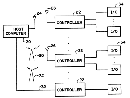
Fig. 1 illustrates a communication system
havinq a host computer and a plurality of process
controllers;
S Fig. 2 is a block diagram of a process
controller shown schematically in Fig. 1:
~ig. 3 is an I/O board for a process
controller having four modular I/O units connected
thereto;
Fig. 4 is a side view of a modular I~O
unit;
Fig. 5 is a circuit diagram of a digital
input circuit shown schematically in Fiq. 2;
Fig. 6 is a circuit diagram of an analoq
input circui~ shown schematically in Fig. 2;
Fig. 7 is a circuit diagram of a digital
output circuit shown schematically in Fig. 2;
Fig. 8 i~ a circuit diagram of an analog
output circuit shown schematically in Fig. 2;
~ig. 9 is a circuit diaqram of a
temperature transducer circuit shown ~chematically
in Fi~ 2;
Fig. 10 is a flowchart of an I/O routine
executed during operation of the process controller;
~ig~ 11 is a flcwchart of an A/D ~heck
routine periodically execu~ed during operation of
the proces 3 controllar, and
Fig. 12 is a flowchart of a change module
rou~ine that allows an operator to change the
position of the ~O modules within the process
controller.
7 c3~ 4
21-56(10739)A
Detailed Description of the Preferred Embodiments
A communication system is illustrated in
~ig. 1. The communication system includes a host
computer 20 and a plurality of process controllers
22 at a number o locations remote from the computer
20. The host computer 20 periodically communicates
with each of the controllers 22 via radio
communication. To this end, the ho~t computer 20
ha~ an antenna 24 and the controllerR 22 have
antennas 26. In order to enhance radio
communication, the communication system may include
a plurality of radio repeaters 30. Instead of
utilizing radio communication, the communication
system may use other types of communication links,
such as a telephone line 32 interconnecting the ho~t
computer 20 with the controller3 22.
The controllers 22 are connected to a
plurality of I/O device~ 34. The I/O devices 34 may
be any type of devices that are either driven by
29 analog or digital signals or that sense conditions
and generate analog or digital signals in response
to the conditions sen ed. Example~ of I/O devices
include pump~ which may be ~urned on or off, valves
th~ po~ition~ of which are incrementally variable,
te~pe~atur~ and pres~ure transduc~rs, etc.
In operation, each of the controllers 22
co~municates with the I/O device~ 34 to which it is
connected to control the process for whi~h that
controller is used. As a simple example, one of the
con~roller~ 22 may be connected to ~wo I/O devices
34, one being a fluid level transducer (not shown)
for sensing the level of fluid within a tank and the
3 ~'~
8 21-56 (10739) A
other being a valve (not shown) within a pipeline
connected to the tank. The fluid level transducer
would generate and transmit to the controller 22 an
analog input signal, and the controller 22 would
control the level of fluid within the tank by
sending an analog output signal to the valve to
control the position of the valve. Such control
could be any type of conventional control, such as
proportional (P) control, proportional-plus-integral
~PI) control, or proportional/integral/derivative
(PID) control.
In addition to performing control
function4, the controllerq 22 perform data-gathering
functions by storin~ various data in memory. Such
data might include the magnitude of the tank fluid
levels over a predetermined period of time.
The controllers 22 periodically
communicate with the host computer 20. This
periodic communication may relate to the control of
the I/O devices 34, or it may be for the purpose of
gathering data from the controllers 22 for storage
in the host computer 20.
A block diagram of the electronics of one
of the p~ocess controllers 22 i9 illu~trated in Fig.
2. The overall operation of the controller 22 is
cont~olled by a microproceqsor 40 which executeq a
computer p~ogram stored in a read-only memory (RO~
42. The microproceq~or 40 and the ROM 42 are
connected to a random-access memory (RAM) 44 and an
EEPROM 45 by mean of a data bus 46 and an address
bus 48. The RAM 44 functions as general purpose
memory and also may be used tO store historical data
20 J73~
21-,6(10739)~
generated by the I/O devices 34. Alternatively,
historical data may be stored in a removable memory
module like the one described in a patent
application entitled, "Process Controller With
Removable Memory Module," U.S. Serial No. 07/6~2,938
~iled12/lllg~ the disclo~ure of which is incorporated
herein by reference. The RAM ~4, which is a
volatile memory, may be backcd up by one or more
batterie~ ~o that data is not lo~t in the event of a
power failute. Th- EEPROM ~S, which i~ a
nonvolatile memory, may be used to store sy~tem
initialization and/or configuration data.
The microprocessor 40 i~ connected to a
bidirectional buffer 50 via a bidirectional bu~
5~. ~he buffer 50 is connected to a plurality of
l/O circuit~ 60 via a bidirectional bus 62.
Although only four r~o circuits 60 are shown in ~ig.
2, there would bc at least one I/O circuit 60 or
each of the I/O device~ 34 to which the controller
22 w~ connected. Flg. 2 illu trate~ the four ~asic
types of I/O c$rcuit , which includ- an analog input
(AI) circuit 60a, an analog output ~AO) circuit 60b,
a dlgital input (DI) circuit 60c, and a digital
output (DO~ circuit 60d. A temp-rature transducer
clrcuit 64 i~ connected to the bus 54. A~ described
in more data~l bolow, the microproce~sor 40
compensate~ th- analog value generated by the analo~
input circuit 60a ~ased upon the analog temperature
value supplied by the transducer circuit 64.
The manner in which the r/O circuit~ 60
ar~ structurally implemented in che controller 22 is
illu~trated in Fiq. 3. Each of the r/o circuit~ 60
2~3~3~
21-56~10739)~
is provided within a separate housing 66, which ~ay
be plastic housings for example. The combination of
the I/O circuit 60 within the housing 66 is referred
to herein as an I/O module 68. The I/O modules 68
are releasably mounted on a printed circuit board
70, which i~ referred to herein as an I/O board.
Each of the I/O modules 68 has two row~ of connector
pins 72 as shown in Fig. 4.
Each module 68 may be inserted into a
respective connector or socket 74 in the I/O board
70. Each socket 74 ha~ two rows of holes or
apertures represented by the lines 76, 78 provided
to match the pattern of connector pins protruding
from each of the I/O modules 68. Each module 68 is
secured to the I/O board 70 by a screw 82 in the
module 68 and a respective threaded bore 84 in the
I/O board 70. The I/O board 70 also ha~ ~ connector
86 for electrically connecting each of the I/O
modules 68 to the bu~ 62 (~ig. 2), or to the I/O
devicea 34, a~ the case may be. The specific manner
of connecting the I/O module 68 to the I/O board 70
is not considered important, and different manners
of connect~on could be used.
While only four I/O modules 68 are
illustrated o~ the I/O board 70 in Fig. 3, more
module~ 68 could be provided in the empty sockets
74, whlch are provided in groups of four. The r/o
board 70 thu~ may have a capacity of at least 16 r/o
modules .
It should be appreciated that each of the
sockets 74 is identical, and that the connector pins
72 protrude from the differen~ I/O modules 68 in
~Q~73~
21-56 ( 10 739 ) A
identical fashion, regardless of the type of I/O
module. Thus, any of the four types of r/o modules
68 can be inserted into any of the sockets 74 in the
I/O board 70. As a result, the I/O board 70 can
S carry any combination of I/O modules 68. For
example, if the I/O board 70 had 16 ~ockets on it,
the I/O board 70 could carry 16 analoq input
modules, or 9 analog input modules and 7 analog
output modules, or 13 digital input module~ and 3
digital output modules, etc.
While Fig. 2 illustrates only four I/O
circuits 60, it should be appreciated that more I/O
circuits 60 would typically be used, and that all
such I/O circuits would be connected to the
lS microprocessor 40 via the buffer 50. The buffer 50
could be implemented with a plurality of
bidirec~ional buffers, or a plurality of
unidirectional buffers. It should also be
understood that the controller 22 could contain
multiple I/O board~ 70 so as to provide more I/O
modules 68. Alternatively, the I/O modules could be
mounted on the same printed circuit board a~ the
micr~proces~or 40.
The microprocessor 40 periodically reads
from or writes to each of the I/O modules 68 at 2
predetermined rate, ~uch as 20 times per second for
example. The manner in which this is performed is
desc~ibed below in connection with Fi~s. S-8, which
are circuit diagrams of the four I/O circuit~ 60a-
60d, and Fig. 10, which is a flowchart of a portionof a computer program stored in the ROM 42 that
controls the communication with the I/O module~ 60.
2~3~
-- 1 2 --
21-56 ( 10 739) A
Diqital Input Circuit
Now referring to Fig. 5, a circuit diaqram
of the digital input circuit 60c is shown. The
digital input (DI) circuit includes a pair of
conductors or lines 102, 104 which are electrically
connected to one of the I/O device~ 34. Although
the lines 102, 104 are shown terminating at the
bottom portion of the I/O module hou~ing 66,
suitable connectors and cabling ~not shown) connect
the lines 102, 104 to the I/O device 34. The I/O
device 34 generates either an open circuit or a
short circuit acros~ the lines 102, 104, depending
upon the state of the condition being monitored. If
the I/O device 34 generates a short circuit acro~s
the lines 102, 104, a current path is created from a
~upply voltage V throu~h a diode 106, a resi~tor
108, a light-emitting diode 110, and through the
lines 102, 104 to ground. A zener diode 112 is
provided b~tween the lines 102, 104 for surge
protection.
~ue to the current flow, the light-
emitting diode 110 turns on a tran~istor 118 which
pull~ down the voltage at the input A4 of a buffer
circuit 120. In the absence of current through the
transi~tor 118, the vol~a~e at the buf~er input A4
i~ norm~lly high due to its connection to a supply
voltage V through a resistor 124.
If the I/O device 34 does no~ generate a
3U short circuit across the lines 102, 104, the light-
emitting diode llO is not illuminated, and the
transistor 118 does not turn on so that the voltage
2~ 73~ i
- 13 - 21-i6(10739)A
at the buffer input A4 remains high.
When the buf~er 120 is enabled via an
enable signal sent to the buffer 120 by the
microprocessor 40 via a line 126, the voltage value
at the buffer input A4 is transmitted to its Y4
output, and to the microprocessor 40 via a line 128.
The buffer 120 also provide~ a second
function of indicating to the microprocessor 40 that
the I/0 circuit 60c is a digital input circuit.
0 Thig i5 accomplished by buffer inputs A0 through A3
being tied to ground. When read by the
microprocessor 40, the Y0 through Y3 output~
associated with the A0 through A3 inputs supply the
binary cod~ 0000 to the microprocessor 40 via four
lS lines 13C. This particular code signifies to the
microprocessor 40 that it i9 communicating with a
digital input circuit.
Analog Input Circuit
A circuit diagram of the analog input
circuit 60~ is illustrated in ~ig. 6. The analog
input circuit 60a ha~ a pair of line~ 162, 164
connected to an I/0 device 34 that complete a
conventional 4-20 milliampere ~ma) current loop
between the analog inpu~ circuit 60a and the I/0
devic~ 34. A current regulator 166 connected to a
supply ~oltage V supplies 25 ma of curr2nt to the
I/0 device 34 via the line 162. A current that
varies between 4-20 ma is supplied from the I/0
device 34 via the line 16~. Thi variable current
is sl~ppl.ed across a resistor 170 to generate a
variable voltage that is supplied to a scaling
_ 14 _
21-56(10739)A
amplifier 172. A pair of zener diodes 174, 175
provide surge protection.
~he voltage generated by the scaling
amplifier 172 is supplied to channel 0 of an A/D
converter 180 via a line 176. The scaling amplifier
172, which may comprise a conventional operational
amplifier circuit, perform4 a scaling function that
ensures that the range of voltages generated across
the resistor 170 i~ about the same as the conversion
range of an A/D converter 180 to provide maximum
re~olution. ln cases where those voltage ranges are
about the same, the scaling amplifier would be
unnecesYary .
Channel 1 of the A/D converter 180 is
connect~d to a li~e 182 which supplies a constant
reference voltaqe. A~ described in more detail
below, the reference voltage is periodically
converted by the A/D converter 180 and read by the
microprocessor 40 to ensure that the A/D converter
180 is functioning properly.
The analog input circuit 60a also includes
a buffer 190 having inputs A0 through A2 connected
to ~round and input A3 connected to a re~atively
high volt~ge vla a resis~or 192. When the enable
input of the bufer 190 is activated by the
microprocessor 40 via a line 194, the buffer 190
trAnsmit~ the binary code 0001 to the microprocessor
40 via four lines 196. aased upon this binary code,
th~ microprocessor 40 can identify ~he I/O circuit
60a as an analo~ input circuit~
A plurality of lines 198 carry clocking
and data signals between the microprocessor 40 and
- 15 - 21-56(10739jA
the A/D converter 180, which may be an LTC1290DCJ
integrated circuit chip commercially available from
Linear Technoloqies. The line 198 connected to the
DI input of the A/D converter 18Q is used to select
the parameters of the converter 180, such as which
channel is to be read, for example. The line 198
connected to the 30 output of the converter 180
transmits in serial fa~hion the multi-bit binary
signal generated by the A/D converter 180 from the
original analog input from the lines 162, 164.
The binary signal, co~responding to the
analog input value, transmitted from the A/D
converter 180 i9 temperature compensated by the
microprocessor 40 based upon the temperature sensed
lS by the temperature transducer 64. This is performed
since the gain of the analog input circuit 60a
varies with temperature.
Digital Output Circuit
A circuit diagram of the digital output
circuit 60d i~ shown in Fig. 7. The digital output
circuit include~ a pair of lines 210, 212 connected
to an I/0 device 34 that is to be controlled by the
digital output value. To control the value of the
digital output, the microproce~sor 40 transmits the
appropriate binary signal ~o the input of a D flip-
flop 220 via a line 222. ~he noncomplemented Q
output of the flip-flop 220 is transm~tted to the
base of a transistor 224 via a resistor 226. When
the Q output i3 hlgh, the transistor 224 turns on,
thus drawing current from a supply ~oltage V through
a resistor 230 and a pair of diodes 232, 234. Upon
3'i~
- 16 - 21-56(10739)A
current flow throuqh the light-emitting diode 234,
the light generated causes a transistor 240 to be
turned on. As a result, current is drawn f rom a
supply voltage V through a current limiter 242,
through a fuse 244 into the output line 210, and
back from the I/O device 34 via the input line 212
to ground. A zener diode 246 is provided for surge
protection.
When the microproce~sor 40 provides a low
voltage signal to the input of the flip-flop 220,
the transistors 224 and 240 do not conduct, thus
preventing any current from bein~ supplied to the
li~e 210.
The Q output of the flip-flop 220 is also
provided to the AS input of a buffer 260 via a line
264 for the purpose of allowing the microprocessor
40 to check to make sure that the flip-flop 220 i~
providing the output that the microproccssor 40
specified via th~ line 222. To this end, upon
~upplying the 3iqnal on the line 222, the
m~croprocessor 40 read~ the Y5 output of the buffer
260 via a line 266 to make sure that it is the same
bin~ry value a~ the signal that was transmitted via
th~ line 222.
The flip-flop 220 is clocked in a
conventional m~nner by the Y~ output of the buffer
260 via a line 270. The Y4 output of th~ buffer 260
i~ con~rolled by its A4 input as supplied by the
microproce~sor 40 via a line 272.
Th~ buffer 260 also ha~ an inpu~ A0 tied
~o a rela~ively hiqh voltage through a resistor 280
and three inputs Al through A3 which are tied to
2~73~
- 17 - 21-56 (10739)A
ground. When enabled via a line 284, the buffer 260
transmits to the microprocessor 40 via the four
lines 286 the binary code 1000 on its Y0 through Y3
outputs. The binary code 1000 signals the
microprocessor 40 that the circuit 60d is a digital
output circuit.
Analog Output Circuit
A circuit diagram of the analog output
circuit 60b is shown in Fig. 8. The analog output
circuit 60b, which generates and transmits an analog
signal to an I/O device 34, includes a digital-to-
analog (D/A) converter 300 having a DATA input
coupled to a line 302 and a CLK input coupled to a
line 304. The microprocessor ~0 specifies the value
of the analog signal to be output to the I/O device
34 by transmitting a multi-bit ~inary signal in
serial fa3hion to ~he DATA input via the line 302.
Upon receiving this binary signal, the D/A converter
300 generate~ a current having a corresponding value
in a pair of line~ 310, 312 connected to its OUTl
and OUT2 output~.
The current i5 provided to a current-to-
voltage ~I/V) converter 320 via the lines 310,
312. The I/V converter 320 generates a voltage
proportional to the input current and transmits the
voltage to a voltage-to-voltage (V/V) converter 322
via a line 324. The V/V converter 322 generates a
voltage on a first output line 326. The line 326 is
also connected to a voltaqe-to-current (V/I)
converter 330, which converts the voltage at its
input to a current and transmits the current to a
~ ~ ~ 7 3 4 _
- 18 - 21-56 (10739) A
second output line 332. A pair of zener diodes 336,
338 are connected between the two output lines 326,
332 and a third output line 340 to provide surge
protection.
~he three output lines 326, 332, 340 are
included to provide flexibility in the types of I/O
devices 34 that the analog output circuit 60b can
control. In particular, I/O device~ 34 that are
voltaqe-driven are connected between the output
lines 326 and 340, whereas I/O devices 34 that are
current-driven are connected between the output
lines 332 and 340.
The output of the I/V converter 320 on the
line 324 is also provided to a buffer 350. The
purpose of buffering the output of the I/V converter
320 i9 to allow the microproce~sor 40 to check the
accuracy of the voltage generated by the I/V
converter 320 to make sure that it corresponds to
the magnitude of the multi-bit binary ~ig~al that
the microprocessor 4Q transmitted to the analog
output circuit via the line 302. The output of the
buffer 350 is provided on a line 352 aQ an AOUT
~ignal. As described below, thi~ AOUT signal is
tran~mitted to an A/D converter in the temperature
traQ~ducer circuit 64 where its value iR
periodl~ally read by the microproce3sor 40.
The analog output circuit 60b also
includes a buffer 354. The buffer 354 has two
input~ AO, Al tied to a relatively hiqh voltage
through a resistor 3S6 and two inputs A2, A3 which
are tied to ground. ~hen enabled via a line 357,
the buffer 35~ transmits to the microprocessor 40
2~ 7 '~''
- l9 - 21-56 (10739)A
the binary code 1100 on its Y0 through Y3 outputs
via four lines 358. ~he binary code 1100 signals
t'ne microprocessor ~0 that the circuit 60b is an
analog output circuit.
s
Temperature Transducer Circuit
Fig. 9 is a circuit diagram of the
temperature transducer 64 schematically shown in
Fig. 2. The transducer circuit 64 includes a
temperature sensor circuit 360 that generate~ an
analog signal on its TEMP output that i~
proportional to the sensed temperature. Since the
sensor circuit 360 is physically located within the
hou~ing of the controller 22, the sensed temperature
is that temperature within the controller housing,
which should be substantially the ame temperature
as the analog input circuit moduleQ 60 since they
are al~o located within the same controller
housing. The sen or circuit 360 may be a
commercially available LT1019 int~grated circuit
chip.
The analog temperatur~ ~ignal generated by
thR temperature sensor 360 is provided to the
noninverting input of an operational amplifier 362
via a line 364. ~he purpose of thc operational
ampli~ier ~62 i9 to amplify the temperature signal
since it ha~ a relatively small voltage (2.1
millivolts/Kelvin).
The output of the opera~ional amplifier
362 is connected to channel 0 of an A/D converter
370 via a line 372. The A/D converter 370 converts
the analQg signal to multi-bit binary form for
~ O ~i 7 3 i L~
2 0 21-56 ( 10 739) A
serial transmission Çrom its 30 output eo the
microprocessor ~0 via the bus 54. Channel l of the
A/D converter 370 is connected to a line 390, which
is connected to receive the AOUT signal from the
line 352 (Fig. 8) via the bus 62. As described in
more detail below, the A/D converter 370
periodically converts the AOUT ~ignal on the line
390 to verify the correct operation of the analog
output circuit of Fig. 8.
The temperature sensor 360 generates a
temperature-compensated reference voltage on its
VOU~ output. Because it i~ temperature compensated,
this reÇerence voltage is constant regardles~ of
change~ in temperature. The compensated reference
voltage i5 supplied to the A/D converter 370.
Supplying the compensated reference voltage to the
A/D conve~ter 370 is advantageou~ since it reduces
any temperature-induced f}uctuations within the
converter 310, thus allowing for more accurate
conversions.
The compensated reference voltage is also
supplied to the noninverting input of an operational
amplifier 376 via a line 378. The amplifier 376
act~ a~ a buffer, and its output on the line 380 is
electrically connected to the line 182 shown in ~ig.
6 via She bus 62 (~ig. 2~ for the purpose o
supplying the reference voltaqe for the A/D
converter 180.
20~73~ i
- 21 - 21-~6(10739).
Operation
During operation of the controller 22, a
number of tasks r~lating to process control are
continuou~ly performed. These tasks and the manner
S in which they are performed are dlsclosed in a
patent application entitled, "Operating System Por A
Process Controller," U.S. Serial No. 07/622,937
filed 12/11/90 the disclo~ure of which i~ incorporated
herein by reference. The task that relates to the
communication between the microprocessor 40 and the
I/O circuit~ 6Q i~ described in detail below.
Upon power up, the microproces~or 40
interrogates each of the I/O module~ 68 to which it
is connected to determine which type of r/O module
is in each of the qocket~ 7~ on the I/O board(~)
70. ~hl~ interrogation entail~ transmitting a code-
reque~t ~ignal, which in thi~ particular ca~e iq a
buffer enable signal, and reading the four-bit
bin~ry code tr~nqmitted b~ the buffer in each I/O
circuit. 8a~ed upon each particular code, the
microproces~or 40 determines the type of each of the
r/O module~ 68 and "remembers" what type each I/O
devic~ i9 by ~toring each code or a similar type
cod~ ln memory. Thu~, the mieroprocessor 40 need
only int~rrogat- the I/O modules 68 once upon power
up~
Afte~ the initial interrogation, the
microorocessor 40 periodically executes an I/O
routine 400 to read from or write to each of th~ I/O
moduleQ 6a. The IJO rou~ine 400 could be performed
20 ~ime~ per seeond, for example.
20~7~4U~
- 22 - 21-56(10739)A
A flowchart of the r~o routine ~00 is set
~orth in ~ig. 10. Each time the ,~O routine 400 is
perrormed, the microprocessor 40 communicates with
each of the I~O modules 68 to which it is
S connected.
~ t step 402, one of the I/O modules 68
which is connected to the microprocessor ~0 is
enabled. This is accompliched by the transmission
of an enable signal from the microprocessor 40 to
the buffer circuit of the l/O module 68. This
enable signal is al~o referred to herein as a code-
reque~t signal since it causes ~he bufer to
transmit the four-bit binary code indicating which
type of l/O circuit 60 the microprocessor 40 is
communicatinq with.
At step 404, the buffer transmits the
~our-bit binary code, indicating the type of I/O
module, and the microprocessor 40 reads that code to
ensure that the proper communication protocol i~
used since each of the four types of I/O module~ 6
has a unique communication protocol.
I the code was ooao, which corresponds to
a di~ital input circuit, step~ 410-gl4, which define
th~ e~m~unication prot~ol uniquely a~ociated with
a digital input circuit, are performed. At step
410, the microprocessor 40 read~ the digital input
on the line 128 (Fig. 5). At step 412, the
microprocessor 40 determineq whether the digital
input is constant for a prede~ermined period of
time. Step 412 is performed tO ensure that
transient signals are ignored. If the signal value
was constant, ~ne program branches t3 step 414 where
J 7 3 i7 ~-
- 2 3 - 21-56 ( 10 739 ) A
the new value o~ the digital input is seored. If
the value waS not constant, the tr~nsient vaiue is
not stored and step 414 is skipped. The program
then branches back to step 402 so that the
microprocessor 40 can communicate with the next I/O
module 68.
If the binary code of step 404
corresponded to an analog input circuit, steps 420-
424 are performed. At step 420, the microprocessor
40 reads the analog input by reading the line 198
connected to the DO output of the A/D converter 180
(Fig. 6).
This analog input tWhich is in multi-bit
binary form) is then compensated based upon the
current temperature reading of the temperature
trancducer circuit 64. The amount of compensation
is based on the gain characteristicq of the analog
input circuit 60a with temperature. The
compensation could be a linear compensation with
temperature or a more complex function. In the
latter case, compensation data could be stored in a
lookup table in a ROM.
Since the temperature inside the hou~ing
of the controller 22 would change relatively slowly,
it i~ not necessary that the microproces~or g0 read
~h~ temperature signal from channel 0 of the ~D
converter 370 ( Fiq . 9 ) each time the I~O routine 400
is executed. It would be sufficient to read the
temperature signal at a more infrequent rate and
store the results in memory ~or use each time the
I/O routine 400 is executed.
2~73~ ~
- 24 - 21-56 (10739)A
At step 424, the compensated analoq input
value is stored in memory. The program then
branches back to step 402 where the next I/O ~odule
68 is enabled.
s If the binary code of step 404
corresponded to a digital output circuit, steps 430-
442 are performed. At step 430, the microprocessor
40 output3 a digital value to the I/O module 68.
This i3 accomplished by transmitting either a binary
one or a binary zero to the D flip-flop 220 via the
line 222 ~Fig. 7).
At ~tep 432, the microprocessor 40 reads
the line 266 (Fig. 7) to determine whether the
digital output circuit 60d provided the correct
output to the I/O device 34. This is accomplished
at step 434 by comparing the binary value received
on the line 266 with the binary value that was
transmitted on the line 222.
lf the two binary value~ match, indicating
that the output wa~ correct, then the program
brancheq back to qtep 402. If the values do not
match, an alarm is ~et at step g36. The time of the
mi~match i9 th-n recorded in memory at step 438.
Th- particular I/O module 68 which failed in this
manner can al o be recorded.
At step 440, if the mismatch is not fatal,
the program branche~ ~ack to step 402. Whether or
not a mismatch is "fatal" is determined by a flag
se~ by the op~rator. The setting of the fatal flag
may depend, for example, on the relative importance
of each particular l/O module 68 and/or the
particular process being controlled.
'a~-73~
- 25 - 21-56(13739)~
If the mismatch is fatal, at step 442
control of the process is suspended, and the digital
output value for that I~O module 68 may default to a
particular fail state specified by the operator.
For example, depending on the application, it may be
desirable to have a solenoid-operated valve fail
either open or closed.
If the binary code of step 404
corresponded to an analog output circuit, steps 450-
462 are performed. At ~tep 450, the microprocessor
40 outputs an analog value (in multi-bit binary
form) to the I~O module 68 via the line 302 (Fig.
8).
At step 452 the microprocessor 40 reads
the value of the multi-bit binary signal on channel
1 of the A/D converter 370 tFig. 9). This value
should correspond to the multi-bit binary value that
the microprocessor 40 tran~mitted to the analo~
output circuit 60b via the linc 302.
At step 454, if ~he two binary value~ are
within a relatively small number of binary counts o
each other, they are concidered to match. If there
ls a match, the proqram branches ba~k to ~tep 402
where the next I/O module 68 is written to or read
25 f rom by the microprocessor 40.
If the value do not match, an alarm is
set at step 456. The time of the mismatch is then
recorded at step 458. The particular I/O module 60
which failed can also be recorded.
At step 460, if the mismatch is not fatal,
the program bcanches back to step 402. rf the
mismatch i5 fatal, at step 462 control of the
2~573~
- 2 6 - 21-~6 ( 10 739 ) A
process is suspended, and the analog output value
for that I/O module 60 may default to a particular
fail value specified by the operator.
It should be appreciated that the basic
S r/o routine 400 described above could be implemented
in various ways. ~or example, after the initial
classification of each of the I/O modules 68 upon
power up, the microprocessor 40 could divide all of
the I/O modules 68 into four groups based upon their
type. Each of the groups could then be read in
order, all of the di~ital input circuits being read
first, then all of the analog input circuits being
read next, etc. In this case, the step 404 of Fig.
10 would be a verification step to verify that the
particular I/O module 68 belonged in the ~roup
currently being te~ted.
Alternatively, instead of dividing all the
I/O modules 68 into groups based upon their
classification, the microprocessor 40 could
communicate with the I/O modules 68 based upon their
positions on the r/o board 70. Thus, the
microprocessor 40 could start at one end of the I/O
board 70 and address each I/O module 68 in
succ~sion according to its physical location. In
thi~ case, each successive r/o module 6~ could be a
different type, and the step 404 would be a branch
step, branching to a different one of the four basic
communication protocols for each successive I/O
module 6~.
Of course, the ~our basic types of I/O
modules 68 described above are not the only types
that could be utilized. Other types of modules,
2~73~
- 27 - 21-56 (10739)A
such as pulse input modules specifically designed
~or inputting trains of digital pulses, could be
used. Alternatively, the controller 22 may be used
only to monitor orocess control conditions, in which
case the controller 22 would not require either
analog or digital output circuit~.
A/D Converter Check Routine
During operation of the controller 22, the
A/D converter 180 (Fig. 6) within each analog input
circuit 60a is periodically checked for accuracy,
quch a~ every 10 seconds for example. This is
accomplished by having the A/D converter 180 convert
a known reference voltage to a multi-bit binary
number, and then determining whether that binary
number i3 within an expected range of binary
numbers.
~ or example, assume that the A/D converter
180 convert3 a voltage between 0 and five volts to a
14-bit binary number. The binary number would be
expected to be 0 when the voltage was zero and 4096
when the voltaqe was five volts. If the reference
voLtage providod to the A/D converter 180 during the
ch-ck wa~ precisely 2.5 volts, the expected binary
output of the converter 180 would be 2048. Since
very 5~all ~luctuations are expected, the binary
output could be compared to make sure it is within a
predetermined range by comparing it with a low range
value of 204~ and a high range value of 2052. If
the binary output ~ell within this ranqe, the A/D
converter 180 would be considered to be working
properly.
20~73~
- 28 - 21-56(10739)A
A flowchart of an A/D converter check
routine 500 is shown in Fig. 11. As described
above, the check routine S00 is periodically
performed to check the A/D converter 180 within each
S of the analog input modules 68a. The routine S00,
which illustrates the checking of one A/D converter
180, would be repeated to check each converter
180. The A/D converters 180 could be checked in any
order and at any desired rate.
The check routine begins at step 502 where
the A/D reference value is read by the
microprocessor 40. This reference value, which iq
the reference voltage on channel 1 of the A/D
converter 180 (Fig. 6), is converted to a multi-bit
lS binary number. At step 504, this binary number is
checked to determine whether it iq in a
predetermined range defined by a lower range value
and an upper range value. At step 506, if the
binary value i9 in range, the A/D converter 180 is
operating correctly and the routine end~.
If the binary number i9 not within the
range, an alarm is 4et at step 508. At ~tep S10 the
tim~ of the A/D converter fault i~ recorded as well
as the I/O module 68 containing the faulty A~D
25- converter 180. Recording such fault data may be
useful 3ince the operator may want to know which
historical data may be subject to error. At step
512, if the A/D converter fault is not fatal, the
routine ends. If the fault is fatal, then at step
514 control of the process is suspended.
3 ~r
2 9 21-56 ( 10739) A
I/O ~Yodule Chanqe Routine
Durin~ operation of the controller 22, ~he
operator may install additional I/O modules 68 onto
the I/O board 70, remove modules 68 from the I~O
S board 70, change the positions of the existinq
modules 68, or any combination of the foregoing.
This is accomplished with the use of an I/O module
change routine 600, which is illustrated in ~iq.
12. The operator initiates the change routine 600
by entering a module-chan~e request via a keyboard
(not shown) coupled to the controller 22.
Referring to Fig. 12, upon entry of the
operator' 5 module-change request, at step 602 the
execution of the I/O routine 400 is suspended. At
step 604, a visual prompt i~ generated on the
controller display (not shown) instructing the
operator to ma~e the desired I/O module 68
changes.
The routine remains at step 606 un~il the
operator ha~ made the desired module changes. The
completion of the changes is indicated by the
operator by entering a module change-complete
command. Upon receiving the change-complete
command, the program branches to ~tep 6~8 where all
o~ the I/O modules 68 are read to de~ermine the new
module typeC. Step 608 i the same process that is
performed upon power up of the controller 22 as
described above.
7 ~ ~,
21-56(10739)~
.~any modifications and alternative
embodiments of the invention will be apparent to
those of ordinary skill in the art in view of the
foregoing description of the preferred embodiment.
This description is to be construed ac illustrative
only, and is for the purpose of teaching those
skilled in the art the best mode of carrying out the
inveneion. The details of the structure and method
may be varied substantially without departing from
the spirit of the invention, and the excluqive use
of all modifications which come within the scope of
the appended claims is reserved.