Note: Descriptions are shown in the official language in which they were submitted.
20~7~6
RCC/dap
MATERIAL LEV~L INDICATING APPARATUS WIT~ STATUS
LIGHT AND EXTERNAL TEST F~ATURES
The present invention is directed to devices for indicating
a predetermined level of material in a storage container - i.e., so-
called point-level indicating devices, as distinguished from
continuous level indicating devices.
Bac~ground of tbe Invention
A number of devices have heretofore been proposed and made
commercially available for indicating point-level of material in a
storage container or vessel. For example, U.S. Patent No. 3,625,058
discloses a device of this character in which a tuning fork is
positioned at a predetermined height within the vessel at which
material level indication is desired, and is coupled to a motor for
vibrating the fork. When material is spaced from the fork, the fork
is free to vibrate. However, when the material reaches the level of
the fork and covers the fork, vibration is damped. Thus, the fact
that the level of material in the vessel has reached the height of
the fork may be detected as a function of vibration characteristics
of the fork itself.
U.S. Patent No. 3,834,235 discloses a device in which an
optical probe is positioned at the desired height of material level
detection in the vessel. ~ight energy is directed into the probe
from externally of the vessel. When material is spaced from the
[ ~ ~
20S75~6
probe within the vessel, the difference in indices of refraction
between the probe material and air at the probe tip is such that the
light energy is reflected back out of the vessel for detection. On
the other hand, when material covers the probe tip, the refractive
index differential at the probe tip is so altered that the light
energy is directed into the material. Hence, the fact that material
has reached the level of the probe tip may be detected externally of
the vessel by absence of light energy reflected from the probe tip.
U.S. Patent No. 4,392,032 discloses a device of the subject
character in which the probe takes the form of a paddle positioned
within the vessel at the desired height of material level detection,
and is connected to a motor carried within a suitable housing
externally of the vessel. When the material is spaced from the
paddle, the paddle is free to rotate as driven by the motor. However,
when the material reaches the level of the paddle, paddle rotation
is retarded, and such retardation may be detected externally of the
vessel.
U.S. Patent No. 4,499,766 discloses a material level
indicating device in which a capacitance probe is positioned within
a vessel such that electrical characteristics at the probe vary as
a function of dielectric properties of the material, which in turn
vary as a function of material level. The probe is connected in an
LC resonant circuit to an rf oscillator, and phase shift of the probe
signal is monitored to indicate changes in material level.
2~75~
Objects and Summary of the Invention
Although devices as disclosed in the above-noted patents
have enjoyed substantial commercial acceptance and success,
improvements remain desirable. For example, although such devices
are typically connected to a remote device for indicating operating
characteristics and therefore material level within the vessel, it
is desirable to provide an indication of operating status - e.g.,
application of electrical power and/or operating characteristics at
the probe - at the device itself. This would assist an operator in
determining status at individual vessels in a field of vessels without
having to return to the remote status board. It is also desirable
to providefacilityfortesting operation ofthe devicefromexternally
of the device without having to remove the housing cover. It is
therefore a general object of the present invention to provide these
and other improvements in material point-level indicating devices
of the described character.
Apparatus for indicating level of material in a vessel in
accordance with the present invention includes a probe for placement
in the vessel at a position corresponding to a desired height at
which material level is to be detected. In the various embodiments
of the invention herein disclosed, such probe may comprise a
capacitance probe, an optical probe, a vibration fork, a rotating
paddle or a pair of ultrasonic transducers spaced from each other
across a material gap. Electronic circuitry is coupled to the probe,
and is responsive to operating characteristics of the probe for
sensing a change of such operating characteristics between a first
operating characteristic at which material is spaced from the probe,
2~7~5~
and a second operating characteristic when material is adjacent to
the probe. The electronic circuitry is contained within a closed
housing mounted on the probe, and is connected to a source of
electrical power positioned remotely of the vessel. A pair of status
lamps are positioned on the housing and are coupled to the electronic
circuitry for respectively indicating application of electrical power
to the circuitry and detection of one or the other of the first and
second operating characteristics at which level of material in the
vessel is either spaced from or adjacent to the probe. The circuitry
further includes a switch positioned within the housing, and
responsive to application of energy through the wall of the housing
from externally of the housing, for simulating the second operating
characteristic of the probe independently of actual material level
at the probe. In the preferred embodiment of the invention, the
switch comprises a reed switch responsive to application of magnetic
energy from a permanent magnet or the like external to the housing so
as to simulate such second operating characteristic of the probe and
illuminate the second status lamp.
Brief Description of the Drawings
The invention, together with additional objects, features
and advantages thereof, will be best understood from the following
description, the appended claims and the accompanying drawings in
which:
FIG. 1 is an electrical schematic diagram of one presently
preferred embodiment of the invention in an rf capacitance-type
application; and
205755~
FIGS. 2-5 are electrical schematic diagrams of other
preferred implementations of the invention.
Detailed Description of Preferred Embodiments
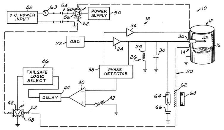
FIG. 1 illustrates apparatus 10 in accordance with one
presently preferred embodiment of the invention as comprising a
capacitance probe 14 mounted on the sidewall of a vessel 12 at a
position corresponding to the height at which it is desired to detect
the level of material 16 within the vessel. Electronic circuitry 18
is carried within a closed housing 20 mounted on probe 14 externally
of vessel 12. The housing and probe construction are illustrated
in greater detail in U.S. Patent No. 4,499,766 noted above. Circuitry
18 includes an rf oscillator 22 that provides a periodic output
signal to a phase shift amplifier 24. The output of amplifier 24
is connected to a parallel LC resonant circuit 26 that includes an
inductor 28 and a capacitor 30 connected in parallel with the probe
conductor 32 of probe 14. Thus, the capacitance probe forms part
of resonant circuit 26. The output of oscillator 22 is also connected
through a unity gain amplifier 34 to the guard shield 36 of probe
14. The wall of vessel 12 is connected to electrical ground.
A phase detector 38 has first and second inputs connected
to the outputs of oscillator 22 and amplifier 24 respectively. The
output of phase detector 38 is connected to the signal input of a
comparator 40, which receives a reference input from a variable
resistor 42. The output of comparator 40 is connected through a
delay 44 to a fail safe logic select amplifier 46 that drives an LED
48. Circuitry 18 is powered by a power supply 50, which in turn
2~57~5~
receives electrical power from a remote d.c. power input source 52
that is connected to supply 50 by a two-wire cable 54. An LED 56
is connected in series between remote power input 52 and power supply
50, and thus indicates application of electrical power to power
supply 50 and the remainder of circuitry 18. LED's 48,56 are
positioned in respective lenses 58,60 in the wall 62 of enclosure 20
so as to indicate status of circuitry 18 externally of enclosure 20.
In operation, LED 56 is illuminated as long as power is
applied to the detection circuitry. Assuming that material 16 is
spaced from probe 14 as shown in FIG. 1, LED 48 is illuminated by
logicselectamplifier 46iflow level fail safe operation is selected,
or is extinguished if high level fail safe operation is selected (as
would be typical). Fail safe logic selection is performed by an
operator usually upon unit installation. Oscillator 22 continuously
applies an rf signal to probe 14 as long as power is applied to
supply 50. Capacitance at probe 14 increases as material level
increases, so that the phase difference between the output of
oscillator 22 and the output of amplifier 24 to resonant circuit 26
correspondingly increases with material level. When this phase
differential, reflected at the output of phase detector 38, reaches
the level of reference 42, the output of comparator 40 switches
accordingly. After delay 44, LED 48 is illuminated by amplifier 46
(assuming high level fail safe selection). In the event that the
level of material 16 in vessel 12 decreases, the phase differential
at detector 38 correspondingly decreases, comparator 40 and amplifier
46 turn off, and LED 48 is extinguished. LED 56 thus indicates
20S7556
application of electrical power to circuitry 18, and LED 48 indicates
point-level operating characteristics at probe 14.
A normally open reed switch 64 is positioned within
enclosure 20 at a preselected position adjacent to enclosure wall
62, and is electrically connected in series with a capacitor 66
across capacitor 30. The capacitance of capacitor 66 is selected to
be equal to or greater than maximum capacitance of material 16 within
vessel 12 when the material is adjacent to probe 14. Thus, when a
magnet 68 is positioned adjacent to reed switch 64 externally of
housing wall 62 so that the magnetic flux from magnet 68 closes the
contacts of reed switch 64, capacitor 66 is connected to resonant
circuit 26. Capacitor 66 thereby simulates operation of probe 14
when the level of material is adjacent to the probe, independent of
actual material level at the probe, so as to test operation of the
remaining circuitry 18. Thus,if circuitry 18 is operating correctly,
positioning of magnet 68 externally adjacent to reed switch 64 should
cause illumination of LED 48. When magnet 68 is removed, LED 48
should be extinguished (assuming that level of material 16 is remote
from probe 14). Circuitry 18 is such that current drawn by the
circuitry through two-wire connection 54 is at one of two essentially
distinct levels, one level being a relatively low current level when
material is spaced from probe 14, and the other being a higher current
level when material is adjacent to the probe and LED 48 is illuminated
by amplifier 46. These two current levels, thus corresponding to
the operating states at probe 14, which in turn correspond to low
and high levels of material 16, may be detected by a meter 69 or
2a~7~sli
other suitable device connected in series between power source 52
and power supply 50.
FIG. 2 illustrates application of the invention in an
electro-optical point-level device of the type disclosed in U.S.
Patent No. 3,834,235. Reference numerals in FIG. 2 (and in FIGS. 3-
5) identical to those employed in connection with FIG. 1 indicate
identical elements. Atransparent probe 70 is mounted on the sidewall
of vessel 12 at a position corresponding to desired height of material
level detection. Probe 70 comprises an optically transparent element
having a tapering end or tip 72. Housing 20 is mounted on probe 70
externally of vessel 12, and level detection circuitry 74 is contained
within housing 20. Circuitry 74 includes a pulse generator 76 that
receives power from remote supply 52 through meter 69, two-wire
interconnection 54 and LED 56 connected in series. The output of
pulse generator 74 is connected to a light source, such as an LED
78. LED 78 is so positioned with respect to probe 70 as to direct a
beam oflight energythroughthe probeto probe tip 72. A photodetector
80 is likewise positioned with respect to probe 70 so as to receive
light internally reflected from tip 72. The output of detector 80
is connected through a normally closed reed switch 82 to a frequency-
to-voltage convertor 84. The output of convertor 84, which is a
d.c. voltage that varies as a function of frequency of input pulses,
is fed to a Schmitt trigger 86. A single-pole double-throw switch
88 has one switch contact connected to the output of Schmitt trigger
86, and a second switch contact connected to the trigger output
through an inverter 90. The common contact of switch 88 is connected
2057~i5~
in series through a resistor 92 and ~ED 48 to the power input to
pulse generator 76.
In operation, pulse generator 76 drives LED 78 and generates
pulses to probe 70 as long as power is applied to circuitry 74. When
material 16 is below the level of probe 70, as shown in solid lines
in FIG. 2, the difference in indices of refraction at probe tip 72
between probe 70 and the air within vessel 12 is such that the light
energy from LED 78 is internally reflected at the probe tip, and is
incident on detector 80. With reed switch 82 closed, the output
pulses from detector 80 are fed to converter 84, which produces a
voltage level sufficient to trigger Schmitt trigger 86. When material
16 rises to the position shown in phantom, the indices of refraction
at probe tip 72 between probe 70 and material 16 are such that most
or all of the light energy from LED 78 is transmitted into the
material. Detector 80 no longer supplies pulses to convertor 84,
and the output Schmitt trigger 86 changes states. LED 48 is illuminated
at either a high or low level of material 16 in vessel 12, depending
upon position of switch 88. For example, in the position shown in
FIG. 2, LED 48 is illuminated when convertor 84 is deprived of input
pulses from detector 80, indicating a level of material adjacent to
probe 70. Positioning of magnet 68 adjacent to reed switch 82
externally of housing wall 62 opens reed switch 82, and deprives
convertor 84 of input pulses from detector 80 independently of level
of material 16. As in the embodiment of FIG. 1, the current from
supply 52 to circuitry 74 is essentially at two levels, one
corresponding to a level at which convertor 84 receives pulses from
detector 80, and the other corresponding to a condition at which
20~7556
convertor 84 is deprived of such pulses. Thus, point-level of
material 16 relative to probe 70 may be detected by a meter 69
connected between power supply 52 and LED 56.
FIG. 3 illustrates implementation of the invention in a
vibrating tuning-fork device of the type disclosed in U.S. Patent
No. 3,625,058. The material probe in this embodiment comprises a
tuning fork 100 coupled to a drive or transmitting crystal 102.
Crystal 102 is driven by an amplifier 104, which in turn is controlled
by a pulse shaper 106. Pulse shaper 106 receives power from remote
supply 52 through two-wire cable 54. Power-indicating LED 56 is
connected to the output of control amplifier 104. A second crystal
108 is positioned adjacent to crystal 102, and is connected through
a variable time delay resistor 110, and through a pair of jumpers
112,114, to respective inputs of a relay control comparator 116.
The output of comparator 116 is connected through LED 48 to the coil
118 of a relay 120. ~elay 120 has suitable normally open and/or
normally closed switch contacts 122 for connection to circuitry
external to housing 20. A normally open reed switch 64 is connected
across crystal 108, and is positioned internally adjacent to the
wall 62 of housing 20 for coupling to external magnet 68 as desired.
In operation, pulse shaper 106 energizes crystal 102through
amplifier 104 as long as power is supplied by remote supply 52. When
material is spaced from fork 100, the fork is free to vibrate, and
such vibration is sensed by crystal 108. Jumper 112 or 114 is factory
selected (and the other jumper is removed) depending on whether high
level fail safe or low level fail safe operation is desired. When
the material within vessel 12 rises to a level so as to contact
--10--
2a575:~
tuning fork 100, vibration of the tuning fork is effectively damped,
and vibration pulses are no longer received at crystal 108. Thus,
depending upon whether low level or high level operation is desired,
LED 48 and relay 118 are energized during one operating state of
tuning fork 100 and crystal 108, and are de-energized at the other
operating state. A level of material in contact with tuning fork 100
is simulated by bringing magnet 68 into external proximity to reed
switch 64, which closes the reed switch contacts and effectively
grounds the output of crystal 108.
FIG. 4 illustrates implementation of the present invention
in a rotating paddle bin level indicator of the type disclosed in
U.S. Patent No. 4,392,032. The material probe 130 in this
implementation of the invention comprises a paddle connected by a
shaft 132 to a motor 134 positioned within housing 20 externally of
vessel 12. Motor 134 is powered by remote power source 52, which
supplies 120 VAC through two-wire interconnection 54. LED 48 is
coupled to an indicator logic circuit 136, which is connected to
motor 134 and responsive to current passing therethrough to indicate
a stall condition at paddle 130. Likewise, LED 56 is connected to
circuit 136 so as to indicate application of electrical power to
motor 134. Relay 118 is connected to indicator logic circuit 136
through fail safe logic 138. Fail safe logic 138 and indicator logic
136 are disclosed in detail in above-noted U.S. Patent No. 4,392,032.
Power is supplied to logic 138 and relay 120 through normally closed
reed switch 82, which is positioned internally adjacent to wall 62
of housing 20 so as to be responsive to external positioning of
magnet 68 adjacent thereto.
--11--
2~57~
In operation, power is normally applied to motor 134, which
rotates paddle 130 within vessel 132. As long as material is spaced
from paddle 130, the paddle 130 is free to rotate as powered by motor
134. When the material rises to the level of paddle 130, frictional
engagement between the paddle and the material retards rotation of
the paddle, stalling motor 134, and thereby indicating level of
material as a function of the current drawn by the motor. Other
methods of detecting retardation of paddle rotation are disclosed
in U.S. Patent Nos. 2,851,553, 3,412,887, 4,095,064, 4,147,906 and
4,695,685. LED 56 is illuminated as long as power is applied. LED 48
is illuminated when the motor is stalled (assuming high level fail
safe operation is selected, or extinguished if low level operation
is selected).
FIG. 5 illustrates implementation of the invention in an
otherwise conventional point-level device in which material level
is detected when material in a gap between ultrasonic transducers
alters transmission of energy therebetween. Specifically, the probe
140 in the device of FIG. 5 comprises a pair of crystals 142,144
carried within vessel 12 at a position corresponding to the height
at which material level is to be detected. Crystals 142,144 are
spaced from each other (by a suitable means not shown) so as to define
a gap 146 therebetween. Crystal 142 is driven by an amplifier 148
that receives power from a power supply 150. Power supply 150
receives electrical power from remote source 52 by means of two-
conductor interconnection 54. Crystal 144 is connected to the control
input of amplifier 148, whereby the combination of crystals 142,144
form an oscillator that oscillates when material is positioned in
-12-
2~57~
gap 146,enhancing coupling between the crystals, and which terminates
oscillation when material is spaced from gap 146, which is to say
that gap 146 is filled with air. A detection and alarm circuit 152
is responsive to oscillation at amplifier 148 for energizing LED 48
and relay 120 (assuming high level fail safe selection), thereby
indicating presence of material in gap 146. When such material is
absent,relay120is de-energizedand LED 48 is extinguished. Normally
open reed switch 64 is connected across crystals 142,144, and is
responsive to external adjacent positioning of magnet 68 effectively
to short circuit the crystals, and thereby simulate presence of
material in gap 146 independently of actual material level.
Preferably, in all disclosed embodiments, reed switch 64
is positioned within the unit housing, as previously described in
connection with each embodiment. However, it is within the scope of
the invention in its broadest aspect to position such switch means
remotely of the unit, external to the housing, for remote test of
the devices.