Note: Descriptions are shown in the official language in which they were submitted.
2057643
A SYSTEM FOR THE GENERATION OF MODULATED OPTICAL SIGNALS
The present invention relates to optical fibre
communications systems exploiting radiofrequency or
microwave-frequency subcarriers, and more particularly to
a method of and a device for generating amplitude-modulated
optical signals for use in one of these systems.
Optical communications systems of the above type
are employed in broad-band distribution networks, e.g. in
integrated services networks, and use optical fibres as a
broad-band transmission medium. Examples of such systems
and of their applications are described by R. Olshansky,
V.A. Lanzisera and P.M. Hill in a paper: "Subcarrier
Multiplexed Lightwave Systems for Broad-Band Distribution",
Journal of Lightwave Technology, Vol. 74, No. 9, September
1989, pages 1329 and ff.
The purpose of the present invention is to provide
a method of and a device for generating amplitude-modulated
optical signals for use in such systems.
In accordance with the invention a method is
provided of generating amplitude-modulated optical signals,
comprising superimposing, upon the bias current of a
semiconductor laser, variations of an electrical signal
obtained by combining and converting into electrical form
~`
~ 2057~49
a fraction of the output signal of the laser, delayed in an
opto-electronic feedback circuit having a presettable delay
and a presettable low frequency gain lower than but close
to a critical value, and an optical signal, amplitude
modulated at a first modulation frequency, said frequency
belonging to a discrete set of frequencies at which the
intensity of the beam from the laser can be modulated by
reason of the presence of the feedback circuit and being
that modulation frequency that occurs when the variations
of an electrical signal obtained by conversion of the
feedback signal alone are superimposed to the bias current
and when the low-frequency gain is higher than the critical
value.
The invention exploits a phenomenon observed by the
inventors in a semiconductor laser provided with delayed
opto-electronic feedback. Under these conditions the
intensity of the beam emitted by the laser is amplitude
modulated and oscillates at a frequency belonging to a
discrete set of frequencies, which depend on delay r and
low-frequency gain B of the feedback loop. More
particularly the delay ~ determines the possible modulation
frequencies, whilst the absolute value IBI of gain B
determines the actual modulation frequency. Depending on
value IBI, two different laser operation regimens exist:
as long as IBI is lower than a certain critical value Bc,
the intensity of the beam emitted by the laser is modulated
at a frequency fl close to the frequency of laser
relaxation oscillation; if on the contrary ¦BI>BC, the
oscillation take place at a frequency f2 which is the
lowest frequency in the set and is 1/r or 1/2~, depending
on the sign of B. Under these conditions, the power of the
laser output signal is very high. Modulation frequencies
are generally comprised in the radio or microwave frequency
range, and the modulation so obtained presents a very
narrow spectral content.
2057649
~.
A more detailed analysis of the behaviour of a
semiconductor laser with delayed opto-electronic feedback
is reported by the inventors in a paper "Instabilities in
a semiconductor laser with delayed opto-electronic
feedback", optics Communications, Vol. 74, No. 1-2, 1st
December 1989.
Further studies and experiments have led the
inventors to observe that when ¦B¦ is slightly below Bc, the
system becomes very sensitive to frequency f2 and, by
injecting into the laser also a low-power signal amplitude
modulated at frequency f2, the oscillation frequency of the
laser output power changes from fl to f2, whilst the output
signal power remains very high and essentially the same as
the power obtained in the case of oscillation at frequency
fl without any external signal. This high power of the
laser output signal is due to the sum of two effects: the
first is the amplification of the modulated signal due to
the combined action of the detector, the laser and any
interposed amplification circuits, whilst the second is the
presence of the feedback loop which is the main contributor
to the attainment of this high power. The invention
exploits this effect, which for the sake of simplicity will
be hereinafter referred to as the "amplification effect"
even though the output power is in effect independent of
the input power.
According to another feature of the invention, the
fact that, for a given value of ¦ B ¦, modulation takes place
at two different frequencies according to whether or not an
amplitude-modulated signal is injected, is exploited to
obtain a frequency modulation effect in combination with
amplification effect. To achieve this, the amplitude-
modulated optical signal is combined with the feedback
signal only during predetermined time intervals, thus
20~7~9
-- 4
periodically switching the modulation frequency of the
outgoing beam between the first frequency and a second
frequency, which is the modulation frequency determined by
the gain of the feedback loop in the absence of an external
signal.
The invention further extends to apparatus for
generating amplitude-modulated optical signals, comprising:
a) a semiconductor laser;
b) an opto-electronic feedback loop associated
with said laser and receiving a fraction of the laser
output signal, said loop having a presettable delay and a
presettable low-frequency gain having a value very close to
but lower than a critical value;
c) means for combining said fraction of the laser
output signal with an optical input signal to be amplified,
which is amplitude-modulated at a first modulation
frequency belonging to a discrete set of frequencies at
which the intensity of the laser output signal can be
modulated owing to the presence of the feedback loop and is
the frequency at which said intensity is modulated in the
absence of the amplitude-modulated input signal when the
low-frequency gain of the feedback loop is higher than said
critical value; and
d) means for converting the combined optical
signals into an electrical signal, for superimposing the
variations of said electrical signal upon a bias current to
be applied to the laser, and for supplying the resulting
bias current to the semiconductor laser to amplitude
modulate its output signal at the same frequency as that of
the input signal.
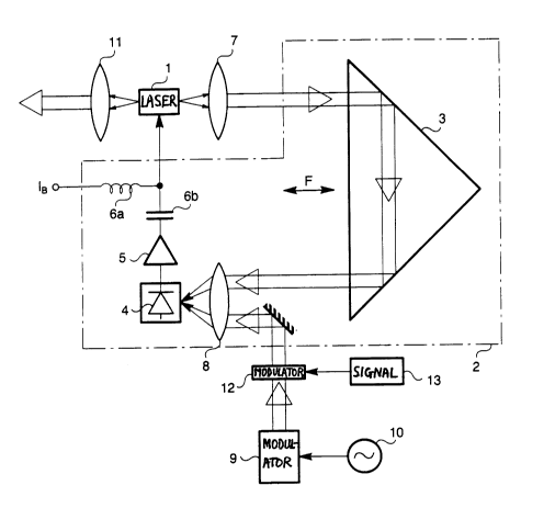
The invention is described further with reference
to the annexed drawing, which shows schematically a device
according to the invention. In the drawing, optical signal
paths are shown by double line arrows, and electric signal
2057649
. .
paths by single line arrows.
A semiconductor laser 1 is biased by a direct
current lB and a signal from an opto-electronic feedback
loop 2, which is supplied with radiation from one face of
the laser 1, e.g. the front face. The feedback loop
comprises:
a) a delay element 3, which introduces delays in
the signal by an externally adjustable delay r. It is
shown schematically by a corner reflector which can be
moved towards or away from laser 1, as shown by arrow F;
b) a detector 4, converting the signal from delay
element 3 into an electrical current;
c) an amplifier 5 amplifying the detector output
current and having an externally adjustable gain; for use
in the present invention, the amplifier gain is adjusted so
that low-frequency gain B of the feedback loop 2 is
slightly lower than the above-discussed critical value Bc;
d) a circuit, comprising an inductance 6a and a
capacitor 6b connected to form a so-called 'bias-tee' as
shown in the drawing, to superimpose photodetection current
variations, originated by the usual fluctuations of the
laser output signal due to noise (e.g. quantum noise due to
the laser structure as well as thermal noise), upon the
laser bias current lB.
Lenses 7, 8 schematically illustrate optical
systems which allow radiation from the laser 1 and
radiation from the delay element 3 to be directed to the
feedback circuit 2 and the detector 4, respectively. The
detector 4 receives also, through lens 8, a low-power
amplitude-modulated optical signal, with a modulation
frequency equal to the above-defined frequency f2, from a
source 9. There are no particular constraints upon the
wavelength of that signal, provided that it lies within the
range accepted by detector 4. Means to effect amplitude
20s764s
modulation utilizing for example a sinusoidal subcarrier at
frequency f2 supplied by a generator 10, are incorporated
in source 9. Techniques by which an optical beam can be
amplitude-modulated are well known in the art.
The modulated optical signal follows the same path
as the feedback signal, and hence the detector output
current will reflect not only variations due to feedback
signal fluctuations, but also those due to the amplitude
modulation of the signal coming from source 9, and these
will be superimposed to bias current lB of the laser 1.
The amplified signal, amplitude modulated at frequency f2,
leaves the rear face of laser 1 and is collected by a lens
11 .
The apparatus described above can be utilized in
several different ways, of which the following are
examples:
a) use as an oscillator at one of the frequencies
determined by the delay and the gain of the feedback loop;
b) use as a narrow band amplifier (by injecting
external low-power signals), with a centre frequency which
can be adjusted externally by acting on feedback loop
delay;
c) use as an injection locked oscillator;
d) use as a modulator to perform frequency
modulation, possibly together with amplification, in a
binary-signal transmission system: the device switches
between frequencies f2 and fl according to whether it
receives the modulated signal (bit 1) or not (bit 0); this
application requires means periodically to intercept the
beam emitted from source 9, such as an acousto-optical
modulator 12 controlled by a square-wave signal supplied by
a generator 13, as shown in the drawing; or the sinusoidal
subcarrier can be electrically modulated by a binary
signal.
-- 20S76~19
Typical values for delay ~ are of the order of a
few nanoseconds, and typical values for Bc are between 1
and 2. The injected signal power depend on the laser
characteristics: typical values may be of the order of 0.1
mW or even less. In an exemplary embodiment of the
invention, source 1 was a commercial single mode laser
detector, 4 was a commercial avalanche photodetector, Bc
was 1.3 (approximately 2.5 dB), ~ was 4 ns, and frequencies
fl and f2 were 970 MHz and 234 MHz, respectively; in
another embodiment, Bc was -1.5 (approximately 3.5 dB), ~
was 5 ns, and frequencies fl, f2 were 660 MHz and 100 MHz
respectively. In both examples, B was set about 0.5 dB
below Bc. The amplification effect obtained exceeded 20
dB.
The embodiment above has been described by way of
non-limiting example, and variations and modifications are
possible within the scope of the invention. More
particularly the device can be implemented by integrated
optics techniques, with modifications which are obvious to
those skilled in the art: in this case the delay ~ may be
much smaller than in the case of discrete components and
the device can thus operate at correspondingly higher
frequencies.