Note: Descriptions are shown in the official language in which they were submitted.
205741
1
INTEGRATED CIRCUIT WITH ANALOG AND DIGITAL
PORTIONS AND INCLUDING THERMAL MODELING
1. Field of the Invention
The present invention relates to an integrated
circuit (IC) and more particularly, to a complementary
metal oxide semiconductor (CMOS) IC which includes an on-
board microprocessor, an analog-to-digital (A/D) subsys-
tem, a communications controller and various input/output
devices on a single monolithic chip for use in various
types of electrical equipment, such as circuit breakers,
motor controllers, contactors and the like for converting
analog signals, such as electrical voltages and currents
to digital signals for monitoring and control. It also
relates to electrical overcurrent circuitry for protecting
electrical equipment, such as electrical motors and the
like, and more particularly, to electrical overcurrent
circuitry for protecting conductors within such equipment
from damage due to overheating which includes digital and
analog modeling of the conductor temperature which enables
the circuitry to simulate a conductor cooling condition
following a trip of the electrical equipment or loss of
electrical power to the electrical overcurrent circuitry.
2. Description of the Prior Art
There has been a recent trend over the years to
utilize digital logic circuitry to control and monitor
various types of electrical equipment, such as circuit
breakers, motor controllers, and the like, in various
industrial, commercial and utility applications. Such
20J~~41
circuitry generally consists of four parts or function
blocks. One function block generally consists of power
supply circuitry to provide a relatively stable voltage to
the IC. Another function block generally consists of a
microprocessor for allowing the control function to be
programmed by a unique set of user generated instructions.
Since many of the conditions to be monitored are analog
(e. g., electrical voltages and currents), an (A/D) con-
verter is necessary to convert these analog values to dig-
ital values. The magnitudes of such electrical voltages
and currents can be on the order of 120 volts and 5 am-
peres, respectively. Because such magnitudes would be de-
structive to most IC's, signal conditioning circuitry is
provided to produce usable values for the IC.
Whether the.four function blocks are included on
a single IC or multiple IC's depends on the state of the
art of the IC processing technologies available. Because
of the ability to match transistors within an IC, for
example, for forming operational amplifiers, for example,
bipolar technology, is generally favored for analog or
linear circuits. CMOS is generally used for digital ap-
plications. However, the current inability to match tran-
sistors relatively closely utilizing a CMOS process has
heretofore made it rather impractical for use in analog
circuits because of the relatively large differential off-
sets created by this inability. Accordingly, given the
superior performance characteristics of the bipolar pro-
cess for analog circuits, the hybrid control analog digi-
tal circuitry for the four function blocks identified
above is generally accomplished with two or more IC's.
However, the use of two or more IC's greatly increases the
cost of the circuitry and also the space requirements be-
cause of the number of components and the interconnections
required therebetween. In many applications, such as in
circuit breakers and motor controllers, space requirements
are at a premium. Thus, the use of a plurality of IC's
dictates that either the circuitry be located external to
2~~'~'~41
the device or the size of the device has to be increased.
Both options are relatively expensive.
In order to take advantage of the performance
characteristics of a bipolar process for analog or linear
circuitry and CMOS for digital circuitry on a monolithic
chip, a hybrid bipolar-CMOS (biCMOS) process for manufac-
turing a single IC has evolved. However, due to the com-
plexity of the biCMOS process, it is relatively expensive.
Another problem with designing hybrid circuitry
for use in control and monitoring electrical equipment is
that such circuitry is often application specific. Thus,
such IC°s cannot be readily adapted for use in applica
tions other than those for which they are designed. For
example, an IC having predetermined functions that are de
signed for use in a circuit breaker, may be inappropriate
for use in a motor controller or the like. Thus, for
various end users with different types of electrical
equipment, separate custom IC's have to be utilized for
each different type of equipment. This can be relatively
expensive.
Various devices are known in the art for
protecting electrical equipment, such as electrical motors
and the like, from damage due to conductor overheating.
Examples of such devices include circuit breakers,
overload relays, motor protectors, and the like. Such
devices are intended to limit the temperature rise of the
conductors within the electrical equipment (e. g., rotor
and stator windings of an electrical motor) to prevent
damage due to overheating. More specifically, current
based time curves, known as overload protection curves,
are normally provided by electrical equipment manu-
facturers which provide the maximum tripping times as a
function of the electrical current that the conductors
can withstand without exceeding the maximum temperature
rise of the conductors and thereby damaging the electrical
equipment.
Overcurrent devices are normally provided with a
tripping characteristic adapted to trip the electrical
20~~941
equipment before the maximum temperature rise is exceeded.
The tripping characteristics of the various overcurrent
devices are provided by various mechanical and electrical
means. Far example, some known overcurrent devices, such
as circuit breakers, incorporate bimetals disposed in
series with the line conductors feeding the equipment
which disconnect the electrical equipment from the source
of electrical power in accordance with predetermined
heating characteristics of the bimetals.
Other known overcurrent devices utilize elec-
tropic tripping and may incorporate a microprocessor to
generate a current based time function based on the
maximum temperature rise of the conductors in the elec-
trical equipment to be protected. Such devices normally
include sensors for sensing the electrical current to the
electrical equipment in order to approximate the conductor
temperature. In such devices for a given overcurrent
value, known as a pick up value, a timing function is
initiated. If the overcurrent condition persists for a
sufficient period of time, the electrical equipment is
tripped. If, however, the current drops below the pick up
level during the time out period, the timer is generally
decreased to a value corresponding to the value at the
pick up level to simulate a conductor cooling condition.
This allows the overcurrent device to provide protection
based on the actual conductor temperature. Should the
power supply to the electrical overcurrent device be lost
following a trip of the electrical equipment, all timing
functions executed by the microprocessor axe generally
lost.
Analog timing circuits including a capacitor
have been used to keep track of the time that the elec-
trical power supply has been lost. More specifically, in
such known devices, every time a trip is initiated a trip
flag is set by the microprocessor and stored. While
power is available, the capacitor is charged to a fixed
value. On power up of such an overcurrent device, the
trip flag is normally checked to determine if a trip
24~'~~~1
occurred. If so, the voltage across the capacitor is
sensed and used to calculate the elapsed time that the
power supply to the overcurrent device was lost. Once the
elapsed time is calculated, the microprocessor then
5 calculates the cool down temperature in order to adjust
its timing function to correspond to a conductor cooling
condition.
Under certain conditions, the power supply to
the electrical overcurrent device may be lost without a
10, corresponding trip of the electrical equipment. Such
conditions may include a trip of an upstream circuit
breaker in a radial feed system. In other known applica-
tions, the overcurrent circuitry is powered by the
circuit breaker being protected. Thus, in such applica-
tions, the power supply to the overcurrent circuitry is
lost when the circuit breaker is tripped. Under such
conditions, the circuitry heretofore described would be
unable to simulate a conductor cooling condition which
could result in damage to the electrical equipment to be
protected.
SUNf~~ARY OF THE INVENTION
It is an object of the present invention to
solve the problems associated with the prior art.
It is another object of the present invention to
provide circuitry capable of controlling and monitoring
various types of electrical equipment, such as circuit
breakers, motor controllers, and the like.
It is a further object of the present invention
to provide analog and digital circuitry for controlling
and monitoring electrical equipment with no interconnec
tions therebetween.
It is yet a further object of the present inven-
tion to provide analog digital control circuitry for con-
trolling and monitoring electrical equipment, which can
rather easily be located in existing space in such equip-
ment.
~~5~~41
It is yet a further object of the present inven-
tion to provide monolithic circuitry for controlling and
monitoring various types of electrical equipment.
It is yet another function of the present inven
tion to provide monolithic CMOS circuitry for controlling
and monitoring various types of electrical equipment.
It is yet another object of the present inven-
tion to provide standardized circuitry which can be uti-
lized with various types of electrical equipment.
It is yet another object of the present inven
tion to provide electrical overcurrent circuitry that is
adapted to simulate a conductor cooling condition follow
ing a loss of electrical power to an electrical overcur
rent device during an overload or subsequent to a trip of
the electrical equipment.
It is yet another object of the present inven-
tion to provide overcurrent circuitry which includes
analog circuitry which simulates both a conductor warming
condition and a conductor cooling condition while power is
available to the overcurrent circuitry.
Briefly, the present invention relates to a
monolithic IC, that is standardized for controlling various
types of electrical equipment, such as circuit breakers,
motor controllers, contactors and the like. The IC is a
monolithic IC, fabricated in CMOS technology. The short-
comings of utilizing CMOS technology for linear or analog
circuitry is overcome by the implementation of the IC to
provide a monolithic IC that is relatively less expensive
than using multiple ICs or a single IC fabricated from
biCMOS technology. Also, by utilizing a single IC, such
control and monitoring circuitry can be located in exist-
ing electrical equipment. The IC in accordance with the
present invention includes an on-board microprocessor, an
A/D subsystem, a communications controller and various
input/output devices which make it suitable for use in
various types of electrical equipment. In order to
improve the resolution of the A/D subsystem, circuitry is
provided, which includes current and voltage ranging
2~5'~~41
amplifiers for ranging analog input voltage and current
signals and compensating internal offsets in such
amplifiers inherent in CMOS linear circuits which can
affect the accuracy of the least significant bits. The
ranging circuitry is controlled either automatically or by
software to provide additional resolution of the A/D
subsystem. The current ranging circuit includes a divider
for dividing analog input signals into a plurality of
composite portions in parallel between an input and output
of the current divider. Novel auto-zero circuitry is
provided for controlling the offsets in the ranging
amplifiers. More specifically, the auto-zero circuitry in
accordance with the present invention controls internal
bias currents within the amplifiers without the need or
expense of~precision resistors as is known in the art.
The communications controller allows the IC to be con-
figured in either a master mode or a slave mode. Thus,
multiple IC's, configured in different modes, can be used
to communicate over different communications networks.
Another important aspect of the invention relates to the
various types of network instructions to which the
communications controller may respond. For example, the
communications controller may respond to FAST STATUS
commands. When such a command is received by the communi-
cations controller, it may respond independent of the on
board microprocessor to improve network response time.
The communications controller is also adapted to receive
UNIVERSAL and BLOCK instructions. UNIVERSAL instructions
are instructions which all devices on the network receive
simultaneously. BLOCK instructions are instructions in
which a block of predetermined devices on the network are
adapted to receive simultaneously.
Briefly, the present invention also relates to
electrical overcurrent circuitry for protecting electrical
conductors in electrical equipment, such as motors and the
like, from damage due to overheating. The electrical
overcurrent circuitry provides both digital based modeling
and analog based modeling of the temperature of an
CA 02057941 1999-O1-18
8
electrical conductor to simulate the conductor
temperature during all expected operating conditions
including a condition when electrical power is
unavailable to the electrical overcurrent circuitry. When
electrical power is available to the circuitry, the
conductor temperature is calculated from the sensed load
currents to form the digital based model. During such a
condition, the analog based model is forced to track the
digital based model. Once the temperature of the
electrical conductor exceeds its maximum safe operating
temperature, the electrical overcurrent circuitry
initiates a trip of the circuit breaker. Since the
overcurrent circuitry is powered either by the sensed
load currents or derived from the circuit breaker output,
the circuit breaker trip will result in a loss of
electrical power to the electrical overcurrent circuitry.
This causes the digital based model to be reset to a cold
conductor temperature value. However, the analog based
model continues to operate to simulate the conductor
temperature during this condition. When electrical power
is restored to the circuit, for example, when the circuit
breaker is closed, the digital model is initialized with
the value from the analog model.
Accordingly, in one aspect, the present
invention provides a CMOS monolithic circuit for
communicating over a communications network comprising:
an analog subsystem including means for receiving analog
signals; a digital subsystem including means for
receiving digital message signals comprised of a
predetermined number of serial bits and including an
CA 02057941 1999-O1-18
8a
instruction portion and an address portion; processor
means for producing digital output signals responsive to
said analog subsystem or said digital subsystem; and
means for transmitting said digital output signals over
said communications network, and including means for
transmitting a predetermined digital message over said
communication network in response to a preselected
instruction portion of a received message signal
independently of said processor means.
In a further aspect, the present invention
provides a device which includes a CMOS monolithic
circuit for monitoring analog signals from an electrical
device having an operate mode and a trip mode and
generating an output signal and communication said output
signal over a predetermined communications network, said
CMOS monolithic circuit comprising: means for receiving
analog signals; processor means for generating digital
output signals as a function of said analog signals and
including a digital status signal indicating a status of
said device; and means for communicating said digital
output signals over a predetermined communications
network, and including means for storing said digital
status signal generated by said processor means and
transmitting the stored digital status signal over the
predetermined communication network independent of said
processor means in response to a message received over
said predetermined communications network having a
preselected instruction portion.
In a still further aspect, the present
invention provides a CMOS monolithic circuit comprising:
an analog subsystem including analog receiving means for
receiving analog signals; a digital subsystem including
digital receiving means for receiving digital signals;
producing means interconnected with said analog receiving
CA 02057941 2001-12-12
8b
means and said digital receiving means for producing an
output signal responsive to said analog subsystem or said
digital subsystem; and means for resetting said digital
subsystem responsive to said analog subsystem and said
digital subsystem.
In a further aspect, the present invention
provides an electrical device comprising: a CMOS
monolithic circuit having an analog portion and a digital
portion, said digital portion having a digital generator
which generates digital output signals as a function of
analog signals received from said analog portion; a
circuit for receiving a differential input signal, a
generator for generating an output signal that is a
function of said differential input signal and an offset,
said offset being a function of bias current within said
generator, a controller for controlling the bias current
to reduce said offset, said controller including a
divider for dividing said bias current into a plurality
of composite portions, a summer for summing said one or
more of said composite portions of said bias current, and
application means for applying said one or more of said
composite portions of said bias current to said generator
to reduce said offset.
In a further aspect, the present invention
provides a CMOS monolithic circuit comprising: means for
receiving analog input signals including analog-to
digital converter means and voltage ranging means for
ranging said analog input signals to a predetermined
range to improve the resolution of said analog-to-digital
converter means; and means at least for producing
digital output signals as a function of said analog input
signals.
CA 02057941 2003-10-08
8C
In a still further aspect, the present
invention provides an electrical device comprising: a
CMOS monolithic circuit having an analog portion and a
digital portion, said digital portion having a digital
generator which generates digital output signals as a
function of analog signals received from said analog
portion; a circuit for receiving a differential input
signal, a generator for generating an output signal that
is a function of said differential input signal and an
offset, said offset being a function of bias current
within said generator, a controller for controlling the
bias current to reduce said offset, said controller
including a divider for dividing said bias current into
one or more composite portions, a summer for summing said
one or more composite portions of said bias current, and
application means for applying said one or more composite
portions of said bias current to said generator to reduce
said offset.
DESCRIPTION OF THE DRAWINGS
These and other objects and advantages of the
present invention will be more easily understood with
reference to the accompanying description and drawings,
wherein:
FIG. 1 is a functional representation of an
application of the IC in accordance with the present
invention;
FIG. 2 is a functional block diagram of the IC
in accordance with the present invention;
FIG. 3 is a functional block diagram of a
portion of the analog portion of the IC in accordance
with the present invention;
CA 02057941 2003-10-08
8d
FIGS. 4(a)-4(d) are diagrams of alternate clock generator
connections for the IC in accordance with the present
invention;
20~~~~1
FIG. 5 is a memory address map for the:IC in
accordance with the present invention;
FIG. 6 is a format diagram for configuration
registers CFR and ACFR which form a portion of the IC in
accordance with the present invention;
FIG. 7 is a format diagram for an EEPROM control
register NVCR which forms a portion of the IC in accord-
ance with the present invention;
FIG. 8 is a format diagram for a dead-man con
trol register DMC which forms a portion of the IC in
accordance with the present invention;
FIG. 9 is a format diagram for A/D conversion
interface registers ADZ, AMZ, ADCR, AMUX, ACSF, AVSF and
ADC which form a portion of the IC in accordance with the
present invention;
FIG. 10 is-a format diagram for comparator mode
control registers CMPI and CMPST and the pulse width modu-
lated output control register PWM which form a portion of
the IC in accordance with the present invention;
FIG. 11 is a block diagram of a programmable
timer which forms a portion of the IC in accordance with
the present invention;
FIGS. 12(a)-12(d) are timing diagrams for the
timer of FIG. 11;
FIG. 13 is a format diagram for programmable
timer registers TCRH, TCRL, TARH, TARL, TICH, TICL, TOCH,
TOOL, TCR and TSR which form a portion of the IC in accor-
dance with the present invention;
FIG. 14 is a connection diagram of a serial
peripheral interface (SPI), single master, which forms a
portion of the present invention;
FIG. 15 is a connection diagram of a typical SPI
with multiple masters;
FIG. 16 are clock and data timing diagrams fox
the SPI illustrated in FIG. 15;
FIG. 17 is a format diagram for the SPI inter-
face registers SPD, SPSR and SPCR which form a portion of
the IC in accordance with the present invention;
l0 20~'~~~~.
FIG. 18 is a format diagram-, for the PORT D
interface registers PDC and PDD which form a portion of
the IC in accordance with the present invention
FIG. 19 . is a block diagram of a parallel port
which forms a portion of the IC in accordance with the
present invention:
FIG. 20 is a format diagram for PORT B interface
registers PBC and PBD which form a portion of the IC in
accordance with the present invention;
FIG. 21 is a format diagram for PORT C interface
registers PCC and PCD which form a portion of'the IC in
accordance with the present invention;
FIG. 22 is a format diagram for PORT D interface
registers PDC and PDD which form a portion of the IC in
accordance with the present invention:
FIG. 23 is a format diagram for the communica-
tions controller interface registers ICAH, ICAL, ICM3,
ICM2, ICM1, ICMO, ICSR and ICCR which form a portion of
the IC in accordance with the present invention;
FIG. 24 illustrates the control message and data
message format diagrams for the communication controller
which forms a portion of the IC in accordance with the
present invention;
FIG. 25 is an overall block diagram of the com-
parator subsystem and A/D input subsystems of the IC in
accordance with the present invention:
FIG. 26 is a schematic diagram of the quadcom-
parator subsystem in accordance with the present inven-
tion:
FIG. 27 is a schematic diagram of the address
decode logic for the comparator control registers CMPST
and CMPI and the configuration register CFR in accordance
with the present invention:
FIG. 28 is a block diagram of the analog subsys-
tem in accordance with the present inventionp
FIG. 29 is a schematic diagram of the micropro-
cessor bus interface logic in accordance with the present
invention;
205"~~41
FIG. 30 is a ,schematic diagram of the address
decode logic for the microprocessor bus interface regis-
ters in accordance with the present invention:
FIG. 31 is a schematic diagram of control and
status registers in accordance with the present invention:
FIG. 32 is a block diagram of the analog digital
control logic portions of the IC in accordance with the
present invention;
FIG. 33 is a block diagram of the analog control
l0 logic in accordance with the present invention:
FIG. 34 is a schematic diagram of the current
multiplexes (MUX) control logic in accordance with the
present invention;
FIG. 35 is a schematic diagram of the voltage
MUX control logic in accordance with the present inven
tion;
FIG. 36 is a schematic diagram of the auto-zero
registers in accordance with the present invention;
FIG. 37 is a schematic diagram of a five
microsecond timer in accordance with the present inven
tion;
FIG, 38 is a schematic diagram of the auto-zero
control logic in accordance with the present invention;
FIG. 39 is a schematic diagram of the auto-range
control logic in accordance with the present invention;
FIG. 40 is a schematic diagram of the auto-range
state machine in accordance with the present invention;
FIG. 41 is an overall block diagram of the
analog circuitry in accordance with the present invention;
FIG. 42 is a schematic diagram of the input MU:~
system in accordance with the present invention;
FIG. 43 is a block diagram of the quad compara-
tor system in accordance with the present invention;
FIG. 44 is a schematic diagram of a band gap
regulator in accordance with the present invention;
FIG. 45A is a schematic diagram of a shunt regu-
lator, B+ comparator and a power monitor in accordance
with the present invention:
12 205'~~~1
FIG. 45B is, a schematic diagram of exemplary
external conditioning circuitry and power supply circuitry
for use with the IC in accordance with the present inven-
tion;
FIG. 45C is a schematic diagram of an exemplary
external regulator circuit for use with the IC in accor-
dance with the present invention;
FIG. 46 is a schematic diagram of a biasing
circuit in accordance with the present invention;
FIG. 47 is a schematic .diagram of another
biasing circuit in accordance with the present invention;
FIG. 48 is a schematic diagram of an analog
temperature sensing circuit in accordance with the present
'invention:
~'IG. 49 is a schematic diagram of the ranging
circuitry for the voltage amplifier in accordance with the
present invention;
FIG. 50 is a schematic diagram of the current
mirror and amplifier in accordance with the present inven
tion;
FIG. 51 is a schematic diagram of the current
mirror in accordance with the present invention;
FIG. 52 is a schematic diagram of the offset
correction circuitry in accordance with the present inven
tion;
FIG. 53 is a schematic diagram of the auto-
zeroable voltage and current amplifiers in accordance with
the present invention;.
FIG. 54 is a block diagram of the communication
controller which forms a portion of the IC in accordance
with the present invention;
FIG. 55 is a block diagram of a digital demodu-
lator which forms a portion of the communication con-
troller in accordance with the present invention;
FIG. 56 is a schematic diagram of a master clock
generator which forms a portion of the communication con-
troller in accordance with the present invention;
13
' FIG. 57 is a schematic diagram of a bit phase
timing generator which forms a portion of the communica-
tion controller in accordance with the present invention;
FIG. 58 is a schematic diagram of a receiver
correlator which forms a portion of the communication con
troller in accordance with the present invention:
FIG. 59 is a partial schematic diagram of a
correlator counter which forms a portion of the communica-
tion controller in accordance with the present invention;
FIG. 60 is the remaining portion of the sche-
matic diagram of a correlator counter which forms a
portion of the communication controller in accordance with
the present invention;
FIG. 61 is a schematic diagram of the demodula
for control logic which forms a portion of the communica
tion controller in accordance with the present invention;
FIG. 62 is a schematic diagram of a bit counter
which forms a portion of the communication controller in
accordance with the present invention;
FIG. 63 is a schematic diagram of bus interface
logic circuit for the communications controller which
forms a portion of the communications controller in accor-
dance with the present invention;'
FIG. 64 is a schematic diagram of an address '
decode logic circuit for the communications controller's
bus interface register in accordance With the present
invention:
FIG. 65 is a schematic diagram of the address
registers which forms a portion of the communication con-
trolley in accordance with the present invention;
FIG. 66 is a schematic diagram of a message
register ICM1 which forms a portion of the communication
controller in accordance with the present invention;
FIG. 67 is a schematic diagram of a message
register ICM2 which forms a portion of the communication
controller in accordance with the present invention;
14
FIG. 68 is a schematic diagram of a message
register ICM3 which forms a portion of the communication
controller~in accordance with the present invention;
FIG. 69 is a schematic diagram of a message
register ICMO which forms a portion of the communication
controller in accordance with the present invention;
FIG. 70 is a schematic diagram of control and
status registers which forms a portion of the communica-
tion controller in accordance with the present invention;
FIG.. 71' is a schematic diagram of bits 26°19 of
a shift register which forms a portion of the communica-
tion controller in accordance with the present invention;
FIG. 72 is a schematic diagram of bits 18-2 of
the shift register of FIG. 71;
FIG. 73 is a block diagram of the communication
controller control logic which forms a portion of the IC
in accordance with the present invention;
FIG. 74 is a schematic diagram of the transmit
ter control logic circuit which forms a portion of the
communication controller in accordance with the present
invention;
FIG. 75 is a schematic diagram of a BCH computer
which forms a portion of the communication controller in
accordance with the present invention;
FIG. 76 is a schematic diagram of an address
comparator circuit which forms a portion of the communica-
tion controller in accordance with the present invention;
FIG. 77 is a schematic diagram of an instruction
decoder circuit which forms a portion of the communication
controller in accordance with the present invention;
FIG. 78 is a schematic diagram of a control and
status logic circuit which forms a portion of the communi-
cation controller in accordance with the present inven-
tion;
FIG. 79 is a continuation of FIG. 78;
FIG. 80 is a timing diagram of various strobe
signals utilized in the communication controller in accor-
dance with the present invention;
2~~~~41
FIG. 81 is a timing diagram of a reset signal
utilized in the communication controller in accordance
with the present invention;
FIG. 82 is a pin out diagram of the IC in accor-
5 dance with the present invention;
FIG. 83 is an exemplary current based time curve
for a cold conductor condition;
FIG. 84 is an exemplary current based time curve
for a warm conductor condition;
10 FIG. 85A is an exemplary curve illustrating the
simulated conductor temperature as a function of time for
an entire operational cycle illustrating a digital model
shown in dashed line and an analog model shown in solid
line;
15 FIG. 85B is an exemplary curve illustrating the
load current as a function of time which corresponds to
the operational cycle illustrated in FIG. 85A;
FIG. 85C illustrates exemplary curves represent
ing a thermal model of a conductor cooling condition and a
conductor warming condition;
FIG. 86 is an electronic overcurrent circuit in
accordance with the present invention;
FIG. 87A is a graph which illustrates a simpli
fied curve of the voltage on the capacitor C1 superimposed
on the calculated temperature rise as a function of time;
FIG. 87B is an enlarged portion of the curves
illustrated in FIG. 87A;
FIG. 88 is a flow chart for charging the
capacitor C1 which forms a portion of the electronic
overcurrent circuitry in accordance with the present
invention;
FIG. 89 is a graph similar to FIG. 87A which
illustrates a detailed curve of the voltage on the
capacitor;
FIG. 90 is a schematic diagram which illustrates
the circuitry during a condition when electrical power is
unavailable to the SURE CHIP integrated circuit;
16
FIG. 91 is a flow chart for the circuitry
illustrated in FIG. 86;
DETAILED DESCRIPTION
DEFINITIONS
The following definitions are to be used
throughout:
Bit designations: Bits within a register will
be designated by placing the bit number within square
brackets. For example, bit 5 of register ABC is desig-
riated as: ABC[5]. Bits 5 through 0 of register ABC are
designated: ABC[5...0]. Bits 4 and 5 of register ABC are
designated as ABC[5,4), etc.
Hexadecimal. Base 16 numbers written with a
dollar sign prefix. For example, $0100 = 256 decimal.
High-true: These signals are designated with
the suffix "h" and are defined to be asserted (true or
logical 1) when their electrical level is at or near the
+VDD supply and are defined to be negated false or a logi-
cal zero) when their electrical level is at or near zero
volts direct current (Vdc).
Low-true: These signals are designated by the
suffix "b" and are defined to be asserted (true, or a
logical 1) when their electrical level is at or near zero
Vdc and are defined to be negated (false or a logical
zero) when their electrical level is at or near +VDD
supply.
Input: An input signal is received by the IC
10.
output: An output signal is driven by the IC
10.
Referring to the drawings, the IC in accordance
with the present invention is generally identified with
the reference numeral 10. The circuitry of the IC 10 has
been standardized to enable it to be utilized with various
types of electrical equipment including circuit breakers,
motor controllers, and the like. For illustration and
discussion purposes only, the IC 10 is shown utilized in a
circuit breaker 12 in FIG. 1. The circuit breaker 12 is
1~ 2a~'~~~41
shown as a three phase circuit breaker having phases iden-
tified as °A", "B" and "C". It is to be understood by
those of ordinary skill in the art that the IC 10 is
capable of being utilized with various other types of
electrical equipment, such as motor controllers, con-
tactors and the like.
The circuit breaker 12 does not form a portion
of the present invention. As shown, the circuit breaker
12 is provided with three current transformers 14, 16 and
10, 18. These current transformers 14, 16 and 18 are disposed
on a load side 20 of the circuit breaker 12 to allow the
circuit breaker 12 to be monitored and controlled. The
line side 22 of the circuit breaker 12 is generally con-
nected to a three phase source of electrical energy (not
shown). The load side 20 is generally connected to a
three phase load (not shown), such as an electrical motor.
An important aspect of~the invention relates to
the fact that the IC 10 is current driven as will be dis
cussed below. More specifically, electrical current from
the current transformers 14, 16 and 18 is applied to the
TC 10 by way of conditioning circuitry 19 (FIGS. 1 and
45B). The~conditioning circuitry 19 is used to provide an
electrical current of about 20.microamperes (uA) to the IC
10.
Another important aspect of the invention
relates to an on-board communication. controller 29. This
controller allows the IC 10 to communicate with devices,
such as a panel meter 31 as illustrated in FIG. 1 by way
of a communications network link, such as a twisted pair
33. Another IC 10 or an INCOM chip, as disclosed in U.S.
Patent No. 4,644,566, can be disposed in the remote meter
31 to allow the remote panel meter 31 to be connected in
another network, by way of another communications network
link 35 which includes its own master controller (not
.shown). A general description of a similar communication
controller connected in a network with a master controller
is described in detail in U.S. Patent No. 4,644,566,
CA 02057941 1999-O1-18
18
assigned to the same assignee as the present invention.
A block diagram of the digital portion of an
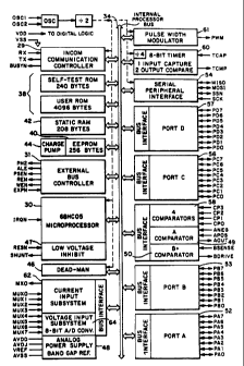
exemplary embodiment of the IC 10 is shown in FIG. 2.
Various configuration options are selectable by software
programming and mask options for specific applications as
will be discussed below. In order to provide an IC 10
with universal application for controlling and monitoring
various types of electrical equipment, such as circuit
breakers, motor controllers, contactors and the like,
various peripherals may be provided. These peripheral
devices may include a microprocessor 30 with a multiply
instruction, for example, a Motorola type MC68H05. The
microprocessor 30 communicates with the various other
peripherals and external pins on the chip 10 by way of an
internal address, data and control bus 34 and an external
bus controller 31. A clock generator 36 provides timing
for the microprocessor 30. An on-board memory subsystem
is provided which may include read only memory (ROM) 38,
electrically erasable read only memory (EEPROM) 40 and
random access memory (RAM) 42. The EEPROM may be provided
with an internal charge pump 44 for obviating the need to
provide an external high voltage source for erasure in
programming of the EEPROM 40.
Exemplary memory sizes are provided for
illustration and discussion purposes only. For example,
256 bytes of EEPROM 40 and 208 bytes of RAM 42 may be
provided. The ROM 38 may include 4,096 bytes of mask
programmable user instruction memory and 240 bytes of
self-test memory.
CA 02057941 1999-O1-18
18a
The IC 10 has separate digital and analog power
supply systems. These power supply systems are segregated
to prevent digital noise from affecting the analog
circuitry. The digital power supply is directed to a VDD
pin on the IC 10 formed from an external voltage
regulator(FIG. 45C). The analog power supply is directed
to a AVDD pin. In many applications, an external
transistor, diode and resistor are adequate.
205'~9~1
Power monitor circuitry 47 is provided, which
includes an internal voltage level detector for monitoring
the gate drive to the shunt regulator associated with the
AVDD pin. The power monitor circuitry 47 deactivates a
SHUNT output pin which, when connected to the RESN input
pin, provides a reset when the analog supply voltage AVDD
begins to fall below a preset threshold. Dead-man cir
cuitry 46 is provided which monitors operation of the
microprocessor 30 and activates a reset upon detection of
spurious operation.
An analog power supply subsystem 48 is provided
for the analog circuitry. This subsystem 48 includes a
+1.25 Vdc band gap regulator and a buffer amplifier to
generate a +2.5 Vdc reference. An external current source
is used to power the analog power supply subsystem 48.
The current source is directed to an external pin AVDD.
An adjustment pin VADJ is provided to allow the voltage
reference to be trimmed to exactly +2.5 Vdc. Trimming may
be provided by a voltage divider circuit, for example, two
series connected resistors connected between the VREF pin
and an analog ground pin AVSS, as illustrated in FIG. 44.
The interface between the series connected resistors is
connected to the VADJ pin. A shunt regulator provides a
nominal +5.0 Vdc source at the AVDD pin based on the
reference voltage at the VREF pin. The buffer amplifier
is provided with an open drain output such that it can
only source current. This will permit multiple devices to
be paralleled. The regulator can also be slaved to
another IC. This is accomplished by connecting the VADJ
pin to the VREF pin on the slave IC and connecting the
VREF pin on the slave IC to the VREF pin on the master IC.
A comparator subsystem is provided which
includes an A comparator 49, a B+ comparator 50 and
quadcomparators 58. The A comparator 49 is for use with
the communication controller 29. A B+ comparator 50 is
provided for external power supply generation as
illustrated in FIG. 45B and discussed below. The invert-
ing input of the comparator 50 is referenced to the VREF
2~ 2057~4i
pin (nominally, +2.5 Vdc). The input signal is applied to
a non-inverting input pin BSENSE of the comparator 50.
The B+ comparator 50 output is connected to an external
pin BDRIVE. The ,quadcomparators 58 include four com-
parators referenced to a fixed voltage, for example +1.25
vac.
Various special functions may also be provided,
such as a timer 60 and a pulse width modulated output 61.
The timer 60 may be used for time base or waveform genera-
tion periodic measurement or other periodic functions.
The PWM output is a periodic signal whose period may be
controlled by the microprocessor's phase 2 clock divided
by 4.
Various other peripheral devices may also be
provided on the IC 10 to allow it to be adapted for
various applications, such as circuit breakers, motor con
trollers and the like. For example, these peripheral
devices may include four general purpose 8-bit bidi
rectional ports: Port A (52), Port B (53), Port C (56) and
Port D (57). A serial peripheral interface 54 (SPI) may
also be provided to allow for efficient connection of
peripheral devices that communicate over a serial bus.
The SPI 54 may also be used for interprocessor communica-
tion in a multiprocessor system. The SPI 54 supports
several operating modes that permit connection of devices
that communicate using various protocols.
An important aspect of the invention relates to
an analog subsystem, identified by the function blocks 62
and 64 in FIG. 2. A block diagram for this subsystem is
illustrated in FIG. 3. The analog subsystem includes, for
example, eight analog input channels for receiving analog
voltage and current signals and converting these signals
to an 8-bit digital signal with 12-bit resolution. Four
of the input channels 62 can be selected by the software
to operate as either voltage inputs or current inputs.
The other input channels 64 can only be operated as volt-
age inputs. Current and voltage input operation of the
21 20~'~~~1
input channels 62 and 64 is controlled by multiplexers
(MUXes) 66 and 68, which are selected by the software.
The voltage input channels can accept positive
voltages in the range of 0-2.5 Vdc and are applied to an
auto-zeroable voltage adjustable gain amplifier 80. These
signals can be processed in either an auto-ranging mode or
a fixed gain mode, selectable by the software. If the
auto-ranging mode is selected, the selected voltage input
channel 62 or 64 is ranged by values stored in an internal
auto-ranging register to allow the gain to be automati-
cally adjusted until the signal is at least' one-half of
full scale but not in overflow. The ranged signal is then
converted directly to an 8-bit digital value by an A/D 78
and stored in an internal register. If fixed ranging is
selected, the voltage mode inputs 62 or 64 can be operated
at preselected gain settings, for example, l, 2, 4, 8 or
16. The preselected gain settings are provided by gain
circuitry which includes a resistor network 84, connected
to an inverting terminal of the voltage amplifier 80 by
way of a MUX 86. The MUX 86 is controlled by the soft-
ware. The output of the voltage amplifier 80 is connected
to the A/D circuitry 78 by way of another MUX 88. The MUX
88 is in the position shown in FIG. 3 when voltage gains
other than one have been selected. However, when a gain
of one is selected, the voltage amplifier 80 is discon
neeted from the ranging circuitry and the input voltage
' channel 62 or 64 is applied directly to the A/D 78.
Current mode inputs 62 accept negative currents
(e.g., currents flowing out of a MXO pin) with a -1.6 mA,
for example, representing full scale. Unselected current
input channels are tied to a digital ground pin (VSS) by
the MUXes 68 which provide for make-before-break switch-
ing. The selected input current channel is connected to
an inverting input of an auto-zeroable current amplifier
90, referenced to analog ground (AVSS). The source
follower output is configured to maintain the inverting
input at a virtual ground by providing current to the
selected channels through an adjustable current mirror 92.
2d~~~~~
22
The current mirror 92 can, be set by auto-ranging cir-
cuitry, which can be overwritten by the software, to one
of the following exemplary ratios: 1/1, 1/2, 1/4, 1/8 or
1/16. The ratioed mirror output current is directed to
the MXO pin. Thus, the current flowing out of the MXO pin
will be a programmable fraction of the sum of the currents
flowing out of the selected current input channel pin.
Two modes of operation are possible:
Non-integrating mode. An external resistor (not
shown) may be connected between the analog ground pin
(AVSS) and the MXO pin to convert the ratioed current to a
voltage. This voltage may then be converted to a digital
value in a similar manner as discussed above. In this
mode of operation, the default amplifier gain is set at
times one unless overwritten by the software.
Integrating mode. An external capacitor (not
shown) may be connected between the analog ground pin
(AVSS) and the MXO pin to integrate the ratioed current.
A shorting switch 96 is provided to discharge this capaci-
for under program control. Integrated voltages are then
converted by the A/D 78 as discussed above.
The voltage and current amplifiers 80 and 90
have offset voltage compensation circuitry 98 to compen-
sate for offsets inherent in CMOS amplifiers. These off-
sets can be on the order of, for example, ~20 millivolt
(mV) which can affect the accuracy of the least signifi-
cant bits of the converted digital value. This circuitry
98 assures that the offset is always a negative voltage
between 0.0 and 0.5 mV and forces the amplifier 80, 90 to
have a positive output when the differential input voltage
is zero. This offset correction can be done either auto-
matically by the hardware or controlled by the software.
Sample and hold capability is provided for the
input channels 62 and 64. More specifically, the eight
analog input channels 62 and 64 are grouped into four
pairs of channels 102, 104, 106 and 107. Each pair of
channels 102, 104, 106 and 107 can be used as a single
channel with sample and hold capability. A capacitor (not
23
shown) may be connected between one channel input and the
analog ground pin AVSS while the other channel of the pair
is connected to a voltage input. A sample command permits
the software to connect the two channels of each pair
together by way of sample and hold MUXes 108, 110, 112 and
114, thus storing the input voltage on the capacitor of
the adjacent channel. Only channel pairs in which both
channels are configured for voltage mode operate in this
fashion. All four channel pairs 102, 104, 106 and 108 may
be sampled simultaneously.
There are other important aspects of the inven-
tion. For example, the IC 10 is adapted to respond to
either analog signals or digital signals and provide a
digital output signal. Another important aspect relates
to the fact that the IC 10 is provided with circuitry
which enables it to sense the ambient temperature in which
it is disposed and generate a corresponding electrical
signal.
OPERATING MODES
The IC 10 has five modes of operation. Two
normal operating modes are single-chip and expanded.
These are selected by strapping an EXPN pin to either the
VSS or VDD pins. The three special operating modes are:
emulation, test and self-check. These modes can only be
selected by connecting certain pins to a voltage level
twice VDD when the reset line is negated. They cannot be
enabled by normal product operation. The operating mode
of the IC 10 is determined by the electrical input levels
of EXPN, IRAN, and TCAP pins when the device comes out of
reset. These pins are sampled when the RESN pin transi-
tions from an electrical low to high. Table 1 defines the
pin input levels for various operating modes.
The operating mode determines the function of
certain device pins: Ai~E, PSEN, REN, WEN and PH2. The
following sections discuss the behavior of the IC 10 in
these different operating modes.
24
TABLE ~
OPERATING MODE SELECTION
Mode EXPN IRON TCAP
Single-Chip VDD VSS to VDD VSS to VDD
Expanded VSS VSS to VDD VSS to VDD
Emulation VDD*2 VSS to VDD VSS to VDD
Test VSS VDD*2 VDD
Self-Check VSS VDD*2 VSS
1. Sinale-chip Mode
The single-chip mode is selected when the RESN
pin changes from an electrical low to high and the EXPN
pin is at VDD. In this mode, Ports A and B operate as
normal bidirectional I/O ports and the microprocessor
executes code from internal mask-programmed ROM. See
Table 2 for operation of variable function device pins.
TABLE 2
PIN DEFINITION FOR OPERATING MODES
Single- Ex- Emula- Test Self
Pad chip panded tion check
ALE low ~ ALE ALE ALE low
PSEN high PSEN LIR LIR high
REN high REN R/W R/W high
WEN high WEN E E high
PH2 low PH2 PH2 PH2 low
2. Expanded Mode
The expanded mode is selected when the RESN pin
changes from an electrical low to high and the EXPN pin is
at VSS. In this mode, Port A becomes a multiplexed
data/address bus and Port B becomes the high-order address
bus. This mode requires program code to reside in an
external memory device. The internal code ROM is not
available and all memory locations above $4000 must be
implemented with external devices. See Table 2 for
operation of variable function device pins.
25 20~'~~41
3. Emulation Mode
The emulation mode is a special operating mode
that is selected by setting the EXPN pin. to a voltage
level twice VDD when the RESN pin changes from an electri-
cal low to high. This mode operates similar to the
expanded mode, except that certain pin definitions change.
See Table 2 for operation of variable function device
pins.
4. Test Mode
The test mode is,used for production testing of
the IC 10. It is selected by setting IRQN at twice VDD
and TCAP at VDD when the RESN pin input rises. See Table
2 for operation of variable function device pins.
5. Self-check Mode
The self-check mode is used for production
burnin. It is selected by setting IRAN at twice VDD and
TCAP at VSS when the RESN pin input rises. See Table 2
for operation of variable function device.
CONFIGURATION METHODS
Since the IC 10 is intended for universal appli
cation of various types of electrical equipment, certain
configuration information is required to tailor the IC 10
for a specific application. The configuration information
is defined by either mask options, software, constants or
run time configuration.
Regarding mask options, the contents of the ROM
38 may be specified at the time the IC 10 is manufactured.
Certain other mask configuration options may be determined
by modification of a single mask. These other configura-
tion options include the dead-man subsystem 46, IRAN trig-
gering, an oscillator option, comparator hysteresis option
and an SPI option. A predetermined hysteresis, for
example, 20 millivolts (mV) or no hysteresis at all can be
selected on an individual comparator basis.
A mask programmable option also permits selec-
tion of the type of interrupt generated associated with an
IRAN pin. One of two triggering methods may be selected
as follows: 1) negative edge sensitive triggering only,
26 2057941
or 2) both negative edge-sensitive and low level-sensitive
triggering. If option 2) is selected, either type of
input to the IRAN pin will produce an interrupt. The IC
can be configured to accept either a crystal/ceramic
5 resonator input or an RC network to control the internal
oscillator. More specifically, the IC 10 can be con-
figured by mask option to accept either a crystal/ceramic
resonator input or an RC network to control the internal
oscillator. The internal cloaks are derived by a divide-
10 by-two of an internal oscillator, which operates with an
AT-cut parallel resonant quartz crystal resonator in the
frequency range of 1 MHz to 8 MHz. Use of an external
oscillator is recommended when crystals outside the
specified range are to be used. The crystal and com-
ponents axe be mounted as close as possible to the input
pins to minimize start-up and stability problems. Table 1
shows recommended parameters for crystal resonators.
A ceramic resonator may be used in place of the
crystal in cost-sensitive applications. The circuit
shown in FIG. 4(a) is recommended when using a ceramic
resonator. Its equivalent circuit is shown in FIG. 4(bj.
Table 3 shows the recommended parameters for various
resonators.
TABLE 3
CRYSTAL/CERAMIC RESONATOR PARAMETERS
CRYSTAL CERAMIC
PARAMETER 2 MHz 4 MHz 2-4 MHz UNITS
RS 400 75 10 ohms
CO 5 7 40 pF
C1 8000 12000 4.3 pF
COSC1 15-40 15-30 30 pF
COSC2 15-30 15-25 30 pF
Rp 10 10 1-10 me~ohms
Q 30 40 1.25 10
A mask programmable oscillator option may be
selected to permit the use of a single external resistor R
between external oscillator pins OSC1 and OSC2 as illu-
strated in FIG. 4(c). With this option, frequencies
between 5 MHz and 70 I~iz are practical. An external clock
2~ 20~'~0~1
input should be used with either mask oscillator option.
This external clock is connected to the OSC1 pin with the
' OSC2 pin unconnected as shown in FIG. 4(d).
Two mask options are available for the SPI.
This mask option selects one of two serial peripheral
interface data pin (MOSI, MISO) configurations.
Bidirectional Data Pins: This configuration
causes the EPI data pins to change direction
when master or slave operation is selected. The
MOSI pin is an output when in the master mode
and an input when in the slave mode. The MISO
pin is an input when in the master mode and an
output when in the slave mode.
a Unidirectional Data Pins: This configuration
forces the SPI data pins to operate indepen
dently of the mode of the SPI. When this con
figuration is selected, MOSI is always an output
and MISO is always an input.
In addition to the mask options, software con
stants are also used for configuration of the IC 10. More
specifically, internal configuration registers are loaded
by the microprocessor software from application dependent
software constants stored in the program ROM 38 or the
EEPROM 40. A pair of internal configuration registers
(CFR, ACFR) are used to control these options in the IC
10. The CFR and ACFR registers are loaded on program
initialization and are not intended to be altered during
normal program operation and will be discussed in detail
below.
Lastly, the IC 10 can be configured by run time
configuration. With this option, configuration data is
read from external devices through the microprocessor's
I/O subsystem. This can be done by utilizing the
input/output ports A, B, C or D in either a parallel or
serial fashion.
CONFIGURATION REGISTERS
The configuration registers CFR and ACFR are
used to specify various software configuration options
28 20~'~~41
available in the IC 10 architecture. These registers CFR,
ACFR are programmed during software initialization to con-
figure input/output pins to their appropriate function as
well as setting other major configuration parameters. In
order to avoid improper operation of the IC 10, the CFR
and ACFR registers should not be altered during normal
operation.
The CFR register is a write only register. The
ACFR register is a read-write register. The bit format
for._the CFR and ACFR registers is illustrated in FIG.
6.
,; ~ Both the CFR and ACFR configuration registers are initial-
ized to zeros on power-up or reset. This defines the
state of the IC l0 after power has been applied and
before
the microprocessor 30 alters it for the application.
CFR REGISTER
The CFR register is a write-only register used'
to configure the comparator output'options. Bits 4
and 5
are unimplemented. The remainder of the bits in the
CFR
register are defined below.
CFR[7]: Communication Subsystem Master Enable.
This is a permissive bit that allows the communication
controller subsystem 29 to be switched into a master
mode.
A zero in this configuration bit prevents the communica-
tion controller subsystem 29 from entering into a master
mode of operation. A one permits master operation.
This
bit is set to zero on reset.
CFR[6]: SPIOFF. This is a disable bit for the
SPI subsystem. When set, the SPI subsystem is disabled.
This bit is set to zero on reset.
CFR[3...0]: Comparator Mode Control. These
four configuration bits enable the comparator outputs
to
be "ORed" with the least significant four bits of port
C.
A zero in these configuration bits enables the OR opera-
tion for the associated port pin. In this mode, each
out-
put pin will be low during device reset if the respective
comparator input is above the threshold voltage (+1.25
V).
Reset will clear the microprocessors PORT C output
regis-
ter, making the output pin only a function of the compara-
29 205'~~41
for input. When the microprocessor writes a "1" into the
. port output register, the output pin will be forced high
independent of the state of the comparator input.
A one in these configuration bits disables the
'OR' operation. In this mode, the port pins are in a high
impedance state after reset. The configuration bits are
assigned in sequential order with CFR[0] controlling scan
PCO/CMPO and CFR[3] controlling PC3/CMP3.
ACFR REGISTER
1.0 The ACFR register is a 7-bit read-write register
and is used to configure the analog subsystem. This
register is set to zero on device reset or power-up. Hit
4 is unimplemented. Bit definitions of the ACFR register
are as follows:
ACFR[7]: Clock Source. This bit selects the
clock source for the A/D 78 and the communication con-
troller subsystem 29 as well as the EEPROM charge pump 44.
They can be configured to use either an internally gener-
ated clock or a clock derived from an external crystal
oscillator of the IC 10: If the crystal oscillator is
selected (ACFR[7] = 1), the oscillator frequency must be
in the range of 2-8 MHz. Other crystal values must use
the internal clock source option (ACFR[7] -. 0)0. If the
communication controller subsystem is used, the external
crystal option must be selected (ACFR7] = 1). This bit is
set to 0 (internal clock source) by reset. A delay of 10
milliseconds (ms) is required after selecting the internal
clock to permit the oscillator to stabilize. During the
stabilization time, A/D 78 and EEPROM 40 operations should
be performed.
ACFR[6]: Divider ratio. This bit selects the
clock divider ratio for the A/D 78 and the communication
controller subsystem 29. There are two considerations
when selecting external crystals and the ACFR[6] setting.
These considerations are: first, the clock input to the
A/D 78 must be in the range of 1-2 MHz; and second, the
clock input to the communication controller subsystem 29
30 20~~~4~.
must be 1.8432 MHz if the communication controller carrier
and bit rate standards are to be met.
This bit, selects a divider ratio of 1/2 or 1/4,
permitting crystals in the range of 2-8 MHZ to be used.
If the communication controller subsystem 29 is active,
either a 7.3728 MH2 or 3.6864 MHz crystal must be used.
The selection of the external crystal and the state of
ACFR[7] will determine the A/D conversion, autoranging and
autozero times. Table 4 defines the configuration bit and
demonstrates the effect on conversion times.
TABLE 4
A/D CONVERTER CLOCK SOURCE
ACFR Crystal A/D Conv.* Auto-zero**
[7,6] Divider (MHz) (~,s) (~,s)
O X Internal NA 48 - 96 13 - 1,537
1 0 1/2 2 48 - 96 25 - 1,537
1 0 1/2 3.6864 . 26 - 52 15 - 884
1 0 1/2 4 24 - 48 13 - 769
1 1 1/4 4 48 - 96 25 - 2,537
1 1 1/4 7.3728 26 - 52 25 - 884
1 1 1/4 8 24 - 48 13 - 769
* The auto-range time depends on the number of gain steps
required to range.
** The auto-zero time depends on the amount of offset
correction required.
ACFR[5]: A/D power-down. This bit controls
power down operation of the A/D subsystem 78. When set,
it will power up the A/D subsystem 78. When the bit is
reset, the A/D subsystem 78 will power down. This bit is
set to zero by reset on power-on. At least 100~s should
be allowed for the converter to stabilize after power-up.
ACFR[3...0]: MUX3...MUXO mode select. These
configuration bits control the input mode of the analog
input channels 62 and 64. The input channels 62
(MUXO...MUX3) can be placed in either a voltage input mode
or a current input mode. A zero in these configuration
bits selects the voltage mode, while a one selects the
current mode. These bits are assigned sequentially with
CA 02057941 2001-12-12
31
ACFR[0] controlling MUXO and ACFR[3] controlling MUX3 as
shown in Table 5.
TABLE 5
ANALOG INPUT MODE DEFINITIONS
ACFR[0] - 0 = voltage mode, 1 = current mode
ACFR[1] - 0 = voltage mode, 1 = current mode
ACFR[2] - 0 = voltage mode, 1 = current mode
ACFR[3] - 0 = voltage mode, 1 = current mode
MICROPROCESSOR 30
The microprocessor 30 is based on a Motorola
type MC68HC05 architecture, a Von Neumann type machine,
which places all data, program and I/0 interfaces into a
single address map. This reduces the number of special
purpose instructions that must be supported and therefore
results in a relatively small and easy to remember
instruction set.
The microprocessor 30 is described in detail in
M6805 HMOS/M146805 CMOS FAMILY USERS MANUAL by Motorola,
Inc., copyrighted 1983,
The microprocessor 30 architecture is based on five regis-
ters: an accumulator (A), an index register (X), a pro-
gram counter (PC), a stack pointer (SP) and a condition
code register (CC).
The accumulator is a general purpose 8-bit
register used by the program for arithmetic calculation
and data manipulations. A full set of read/modify/write
instructions operate on this register. The accumulator is
used in the register/memory instructions for data manipu
lation and arithmetic calculation. The index register is
used in the index mode of addressing or as an auxiliary
accumulator. It is an 8-bit register that can be loaded
either directly or from memory, having its contents stored
in memory, or its contents compared to memory. In index
instructions, the index register provides an 8-bit value
that is added to an instruction provided value to create
an effective address. The index register is also used for
limited calculations and data manipulation.
32 205741
The program counter is a 16-bit register and
contains the memory address of the next instruction that
is to be fetched and executed. Normally, the program
counter points to the next sequential instruction, how-
ever, it may be altered by interrupts or certain instruc
tions. During an interrupt, the program counter is loaded
with the appropriate interrupt vector. Jump and branch
instructions may modify the program counter so that the
next instruction to be executed is not necessarily the
next instruction in memory.
The stack array or stack is an area in memory
used for the temporary storage of important information.
It is essentially a sequence of RAM locations used in a
last-in-first-out (LIFO] fashion. The stack pointer al-
ways points to the next free location on the stack. In-
terrupts and subroutines make use of the stack to tem-
porarily save important information. The stack pointer is
used to automatically store the return address (2 byte
program counter) on subroutine calls and to automatically
store all registers (5 bytes: A, X, PC and CCj during in-
terrupts. The stack starts at location $OOFF and extends
downward 64 locations.
The condition code register is a 5-bit register
that indicates the results of the instruction just exe
cuted, as well as the state of the processor. These bits
can be individually tested by a program instruction and
specified action taken as a result of their state. The
following condition code bits are defined: half-carry
(H), interrupt mask (I), negative (N), aero (Z) and
carry/borrow (C).
MEMORY MAPPING
The microprocessor 30 is capable of addressing
65,536 bytes of memory. Thus, the memory space ranges
from $0000 to $FFFF. FIG. 5 is a diagram of memory allo
cation for the IC 10.
1. ROM 38
The IC 10 memory map has three sections of mask
programmable ROM 38 and accommodate up to 32,768 bytes of
33
external ROM in the expanded mode at locations $8000 to
$FFFF. This memory 38 is programmed at device manufac-
ture. The three sections of the ROM 38 are located as de-
fined in Table 6.
TABLE 6
ROM ASSIGNMENTS
ADDRESS RANGE SIZE FUNCTION
$EF00-$FEFF 4096 bytes User instruction memory
$FF00-$FFEF 240 bytes Self-check program
$FFFO-$FFFF 16 bytes Vectors
2. RAM 42
The IC 10 is configured with 208 bytes of RAM
starting at location $0030 extending to $OOFF and
can ac-
commodate 16,384 bytes of external RAM at locations
$4000
to $7FFF. The top of this internal RAM $0030 to $OOFF
area is reserved for the stack. The stack starts
at loca-
tion $OOFF and extends downward a maximum of 64 locations
to $OOCO. Unused stack locations may be used by the
pro-
gram for general storage. However, care must be exercised
to avoid data being stored in these locations being
over-
written by stack operations.
3. EPROM 40
The IC 10 has 256 bytes of EEPROM 40 located at
addresses $0100 through $O1FF.
4. INTERRUPT AND RESET VECTORS
The upper 16-bytes of the memory map are re-
served for interrupt vectors. The address assignments
for
each are described below:
SFFFE-FFFF: RESET VECTOR
This vector is used on processor reset. It has
the highest priority of the eight interrupts.
SFFFC-FFFD: SOFTWARE INTERRUPT
This vector is used during execution of the SWI
instruction. It has the second-highest priority of
the
eight interrupts.
34 205'~~41
$FFFA-FFFB: EXTERNAL ASYNCHRONOUS INTERRUPT
This interrupt is assigned the third-highest
priority of the eight interrupts. The external interrupt
(IRAN pin) uses this vector.
$FFF8-FFF9: TIMER INTERRUPT
This interrupt is assigned the fourth-highest
priority of the eight interrupts. It is used by the timer
60.
$FFF6-FFF7: COMPARATOR SUBSYSTEM INTERRUPT
This interrupt is assigned the fifth-highest
priority of the eight interrupts. It is used by the com-
parator subsystem 58.
$FFF4-FFF5: A/D SUBSYSTEM INTERRUPT
This interrupt is assigned the sixth-highest
priority of the eight interrupts. It is used by the A/D
78.
$FFF2-FFF3: SERIAL PERIPHERAL INTERRUPT
This interrupt is assigned the seventh-highest
priority of the eight interrupts. It is used by the SPI
subsystem 54.
SFFFO-FFF1: INCOM COMMUNICATION CONTROLLER INTERRUPT
This interrupt is assigned the lowest priority
of the eight interrupts. It is used by the communication
controller 29.
5. DATA TRANSFER AND CONTROL
Data transfer and control functions are imple-
mented using byte-wide register interfaces accessed by the
microprocessor 30 in its memory address space as defined
in Table 7.
EEPROM CONTROL
The microprocessor 30 controls the operation of
the EPROM 40 by a single read-write register NVCR, located
in memory address space. FIG. 7 shows the format of this
register. Reset clears this register to zero. This will
configure the EEPROM 40 for normal read operation. A de-
scription of the bit assignments for the NVCR register is
provided below:
35 205'~~41
TABLE
7
REGISTERADDRESS MAP
ADDR REGISTER, REGISTER ADDR REGISTER
ADDR
$0000 PAD ~ $0010 TSCH $0020 ADCR
$0001 PBD $0011 TSCL $0021 AMUX
$0002 PCD $0012 TCR $0022 ADC
$0003 PDD $0013 TSR $0023 ACFR
$0004 PAC $0014 TICH $0024 ADZ
$0005 PBC $0015 TICL $0025 AMZ
$0006 PCC $0016 TOCH $0026 AVSF
$0007 PDC $0017 TOOL $0027 ACSF
$0008 CMPST $0018 TCRH $0028 ICAH
$0009 CMPI $0019 TCRL $0029 ICAL
$OOOA SPCR $OOlA TARH ~ $002A ICMO
$OOOB SPSR $OO1B TARL $002B ICM1
$OOOC SPD $OO1C NVCR $002C ICM2
$OOOD $OO1D PWM $002D ICM3
$OOOE $OOlE CFR $002E ICCR
$OOOF $OOlF TEST $002F ICSR
$OFFO DMC
NVCR[7...5]: Unused. These bits are reserved
for device testing.
NVCR[4]: Byte Erase Select (BYTE). This bit
selects byte erase operations. When set, it overrides the
row bit. If BYTE is set to a 1, erase operations effect
the selected byte. If BYTE is set to zero, erase opera-
tions are either row or bulk.
NVCR[3]: Row Erase Select (ROW). This bit
selects row or bulk erase operations. If BYTE is set,
this bit is ignored. If ROW is set to a 1, erase opera
tions effect the selected row. If ROW is set to a 0, bulk
erase is selected.
NVCR[2]: EEPROM Erase (ERASE). This bit con-
trols erase operations in the following manner: If ERASE
is set to a 1, erase mode is selected. If ERASE is set to
a 0, normal read or program mode is selected.
NVCR[1]: EEPROM Latch Control (EELAT). This
bit controls EEPROM address and data latch operations as
follows: If EELAT is set to a 1, address and data can be
latched into the EEPROM 40 for programming or an erase
operation. If EELAT is set to a 0, data can be read from
the EEPROM 40. If an attempt is made to set both the
36
EELAT and EEPGM bits in the same write cycle, neither will
be set.
NVCR[0]: EEPROM Program Voltage Enable (EEPGN).
This bit determines the operating mode of the EEPROM 40 as
follows: If the EEPGM is set to a 1, the charge pump 44
is on and the resulting high voltage is applied to the
EEPROM array. If EEPGM is set to 0, the charge pump
generator is off. If an attempt is made to set both the
EELAT and the EEPGM in the same write cycle, neither will
be set. If a write to a EEPROM~address is performed while
the EEPGM bit is set, the write is ignored and the pro-
gramming operation currently in progress is not disturbed.
These two safeguards prevent accidental EEPROM 40 changes.
EEPROM OPERATION
Specifications for the EEPROM 40 are provided in
Appendix A. An internal charge pump 44 avoids the neces-
sity of supplying a high voltage 'for erase and program-
ming. To reduce programming time, bulk, row and byte
erase operations axe supported.
The erase state of an EPROM byte is $FF. Pro-
gramming changes ones to zeros. If any bit in a location
needs to be ganged from a zero to a one, the byte must be
erased in a separate operation before it is reprogrammed.
If a new byte has no ones in bit positions which were al-
ready programmed to zero, it is acceptable to program the
new data without erasing the EEPROM byte first.
Programming and erasure of the EEPROM 40 relies
on an internal, high voltage charge pump 44. The clock
source for the charge pump 44 is the same as the A/D sub
system and is selected by ACFR[7,6] as discussed above.
Clock frequencies below 2 MHz reduce the efficiency of the
charge pump 44 which increases the time required to pro-
gram or erase a location. The recommended program and
erase time is 10 ms when the selected clock is 2 MHz and
should be increased to as much as 20 ms when the clock is
between 1 MHz and 2 MHz. At least 10 ms should be allowed
after changing the clock source for the charge pump 44 to
stabilize.
r~.
37
The EEPROM 40 operation is controlled by the
NVCR register. Various operations are performed by the
EEPROM 40 as described below. Other processor operations ,
can continue to be performed during EEPROM programming and
erasure provided these operations do not require a read of
the data from the EEPROM 40. The EEPROM 40 is discon-
nected from the internal read/data bus 34 during program
and erase operations.
To read data from the EEPROM 40, the EELAT bit
must be zero. When this. bit is cleared, the remaining
bits in the NVCR register have no meaning or effect and
the EEPROM 40 may be read as if it were a normal ROM.
During EEPROM 40 programming, the ROW and BYTE
bits are not used. The zero bits in a byte must be erased
by a separate erase operation prior to programming. The
following sequence of operations is required to initiate a ~
programming cycle as follows:
1. Set the EELAT bit with EEPGM = 0
2. Store data to the EEPROM memory location
3. Set the EEPGM bit to turn on the high voltage
4. Wait 10 ms
5. Reset both EEPGM and EELAT bits to return to
normal operation (clear NVCR)
The following sequence of operations is required
to initiate a bulk erase of the EEPROM memory as follows:
1. Set the ERASE and EELAT bits with EEPGM = 0
2. Write any data to any EEPROM address
3. Set the EEPGM bit to turn on the high voltage
4. Wait 10 ms
5. Reset ERASE, EELAT and EEPGM bit to return to
normal operation (clear NVCR).
A row in the EEPROM 40 is a group of 16 bytes
whose starting address is $xxNO and whose ending address
is $xxNF. The x's indicate don't care address bits. The
N is the row number. This type of erase operation saves
time compared to byte erase operations when large sections
of EEPROM are to be erased. The sequence of operations
38 205'~~41
required to initiate a row erase in the EEPROM 40 is as
follows:
1. Set the ROW, ERASE and EEhAT bits with EEPGM = 0
2. Write any data to any EEPROM address in the
selected row
3. Set the EEPGM bit to turn on the high voltage
4. Wait 10 ms
5. Reset ROW, ERASE, EELAT and EEPGM bit to return
to normal operation (clear NVCR)
DEAD-MAN SUBSYSTEM 46
The dead-man circuitry 46 monitors the micropro-
cessor 30 fox proper operation. This function is a mask-
enabled option that interacts with the microprocessor 30
through a single register (DMC) located at address $OFFO.
The dead-man circuitry may implemented as a 17-bit ripple
counter that provides a timeout period of 32.8 milli-
seconds at a bus rate of 4 MHz (262,144 oscillator
cycles). If the counter overflows, a processor reset will
occur and the device will be reinitialized.
The dead-man timer is reset by writing a zero to
DMC[0]. This will reset the counter and begin the timeout
period again. The location of the DMC register was chosen
such that a normal bit manipulation instruction cannot re-
set the timer. Only extended or indexed, 16-bit offset
addressing modes can access this location.
DEAD-MAN INTERFACE REGISTER
The dead-man subsystem is controlled by a 1-bit
register (DMC) located in memory address space. FIG. 8
defines the register's format.
DMC[0]: Dead-man Reset. This write-only bit is
used to reset the dead-man timer. Writing a zero to it
will reset the dead-man counter and restart the dead-man
timeout time.
ANAIrOG SUBSYSTEM II~1TERFACE REGISTERS
The microprocessor 30 interface consists of
seven registers (ADZ, AMZ, AMUX, ACSF, AVSF, ADC, and
ADCR) located in the memory address space. The format of
these registers is shown in FIG. 9.
39
ADZ: A/D Auto-zero Value. This 6-bit read-
write register contains the offset correction value for
the voltage input amplifier 80. The ADZ register is
loaded with the correction value at the completion of an
auto-zero sequence. A value of zero represents the in-
trinsic positive offset built into the amplifier 80. As
the ADZ value increases, the offset decreases. A least-
significant-bit represents approximately 0.5 mV offset.
The correction value may be changed by writing to this
register. .. Write operations to the ADZ register are in-
tended for diagnostic and verification purposes and are
not intended in normal operation. The auto-zero sequence
should provide the proper offset value for nominal device
operation. At the completion of the auto-zero, the offset
of the amplifier 80 should be in the range of 0 to -0.5
mV.
AMZ: Amplifier Auto-zero Value. This 6-bit
read-write register contains the offset correction value
for the current amplifier 90. The AMZ register will be
loaded with the correction value at the completion of an
auto-zero sequence. As the AMZ value increases, the off-
set decreases. A least-significant-bit represents ap-
proximately 0.5 mV offset. The correction value may be
changed by writing into this register. Write operations
to this register are intended for diagnostic and verifica
tion purposes and are not intended in normal operation.
The auto-zero sequence should provide the proper offset
value for nominal device operation. At the completion of
the auto-zero, the offset of the amplifier should be in
the range of 0 to -0.5 mV.
ACSF: Current Scale Factor. This read-write
register is used to control operation of the current input ,
auto-ranging. The value written into this register deter-
mines the current subsystem auto-ranging operating mode.
If a zero is written, the current subsystem is placed in
auto-ranging mode. A nonzero value inhibits auto-ranging
and sets the current mirror 92 into a fixed scale value.
Table 8 defines possible values for ACSF write operations.
4a 2p~'~~41
Values other than these will cause unpredictable opera-
tion.
This register is not a true read-write register.
The value read from it is not necessarily the value that
was written into it. Writing a zero into ACSF enables
auto-ranging, however, a zero will never be read from the
ACSF register. There are only five possible values that
will be read: $10, $O8, $04, $02, and $O1.
The value read from this register is one of the
scale factors required to properly scale the 8-bit A/D
output. Five values are possible: xl, x2, x4, x8 and
x16. Scale factors are shown in Table 8.
TABLE 8
CURRENT SCALE FACTOR CONTROL VALUES
HARDWARE SOFTWARE
ACSF[7...0~ MODE SCALE FACTOR
$00 Auto-ranging enable
$10 Divide by 16 x 16
$08 Divide by 8 x 8
$04 Divide by 4 x 4
$02 Divide by 2 x 2
$01 Divide by 1 x 1
AVSF: Voltage Scale Factor. This read-write
register is used to control operation of the voltage input
auto-ranging. The value written into this register deter
mines the voltage amplifier 80 auto-ranging operating
mode. If a zero is written, the voltage amplifier 80 is
placed in auto-ranging mode. A nonzero value inhibits
auto-ranging and sets the voltage amplifier 80 in a fixed-
gain mode of operation. Table 9 defines legal values for
AVSF wrLte operations. Values other than these will cause
unpredictable operation.
This register is not a true read-write register.
The value read from it is not necessarily the value that
was written into it. Writing a zero into AVSF enables
auto-ranging, however, a zero will never be read from
AVSF. There are only five possible values that will be
read: $10, $08, $04, $02 and $O1.
41 2057941
TABLE 9
A/D VOLTAGE AMPLIFIER CONTROL VALUES
HARDWARE SOFTWARE
ACSFf7...01 MODE SCALE FACTOR
$00 Auto-ranging enable
$O1 x 16 gain x 1
$02 x 8 gain x 2
$04 x 4 gain x 4
$08 x 2 gain x 8
$10 x 1 gain x 16
The value read from this register is one of the
scale factors required to properly scale the A/D output.
Five values are possible: xl, x2, x4, x8 and x16. Scale
factors are shown in Table 9. This register should not be
read or written to while a conversion is in progress.
AMUX: Input Multiplexer Controls. This 8-bit
read-write register is used to select the MUXes 66 and 68
connected to the voltage and current input channels 62 and
64. The register is divided into two 4-bit fields; one
for controlling the voltage input channels and the other
for controlling the current input channels. It is also
used to initiate the A/D conversion process. Writing to
this register will initiate an A/D conversion.
AMUX[3...0]: A/D Channel Select. These four
bits control operation of the voltage input channels 62
and 64. These bits are decoded as shown in Table 10.
Values indicated as "reserved" are dedicated to test and
verification and should not be selected during normal
operation. When the current channels 62 are selected
(AMUX[3...0] = 1000), auto-ranging of the voltage ampli-
fier 80 will be inhibited and the gain set to xl. If a
nonzero value has previously been written into the AVSF
register, the selected gain will be used instead of an xl
gain factor.
42
TABLE 10
Al D CHANNEL SELECT DECODE
AMtIX AMUX
3...0 SOURCE f3...01 SOURCE
0000 MUXO 1000 MXO (Current Channel)
0001 MUX1 1001 Reserved
0010 MUX2 1010 Reserved
0011 MUX3 1011 Reserved
0100 MUX4 1100 Reserved
to 0101 MUX5 1101 Reserved
0110 MUX6 1110 Temp. Sensor
0111 MUX7 1111 AVSS (0 volts)
AMUX[7...4]: Current MUX Select. These four
bits control operation of the current input channels 62.
Each bit controls a channel independent of the other three
bits. Bits are assigned sequentially with AMUX[4] as-
signed to input pin MUXO and AMUX[7] assigned to input pin
MUX3. These bits have no effect if the associated channel
is configured for voltage mode by the CFR register. A
zero in AMUX[7...4] connects the appropriate input pins)
to digital ground (VSS), while a one connects the pins)
to the current mirror 92 output. The currents can be
summed by selecting multiple current inputs. If all four
bits of this field are zero, no input channels are con-
nected to the current mirror 92 output. Since the invert-
ing input of the current amplifier 90 remains connected to
the current mirror 92 output, the current amplifier 90
output will be low, and the current mirror 92 will have no
current flowing out of it.
ADC: A/D CONVERTER OUTPUT This read-only
register is used to return the 8-bit output value. The
least-significant bit is in ADC[0]. This value must be
multiplied by the voltage and current scale factors found
in ACSF and AVSF. Depending on the mode of operation,
both scale factors may not be needed:
Voltage Inputs: The ADC register should be mul-
tiplied by AVSF for all voltage inputs. The contents of
43
ACSF register should not be used to scale a voltage read-
ing.
Current Inputs: The ADC register should be mul
tiplied by the value in the ACSF register and then the
AVSF register for scaling of the current subsystem output
(MSO). If the voltage amplifier 80 is set to auto-rang-
ing, the AVSF software scale factor will always be x16,
since the voltage hardware gain will be forced to xl by
the selection of MXO.
If an input voltage is converted that is not in
the range of AVSS to VREF, the A/D converter will return
either $00 (voltages less than AGND) or $FF (voltages
greater than VREF). No additional indication is provided.
ADCR: A!D Subsystem Control This byte-wide
register is used to control operation of the A/D 78. It
is implemented as a read-write register to permit read
modify-write instructions to properly manipulate bits.
All command bits will read as zero. Control bits will
read the current value of the control bit.
ADCR[0]: Unused. This bit is not used. The
ADCR[0] bit will always read zero.
ADCR[1]: Sample Inputs. This control bit is
used to close the four MUXes 108, 110, 112 and . 114 that
connect the pairs of channels 102, 104, 106 and 108 to-
gether to form the sample and hold function. The channels
are closed when ADCR[1] - 1 and open when ADCR[1] = 0.
ADCR[1] is set to zero by device reset. Each of the
sample and hold switches 108, 110, 112 and 114 will close
only if both channels it is associated with are configured
in the voltage mode.
ADCR[2]: Initiate Auto-Zero Sequence. When
this command bit is written with a one, the voltage and
current amplifiers 80 and 90 will initiate an autozero se-
quence. When the sequence is completed, the ADCR[6] bit
will be set to a one. An interrupt will be generated, if
enabled, at the completion of the autozero sequence. The
ADCR[2] bit will always read °zero'.
,.....
44 2~~~~~1
ADCR[3]: Integrator Reset. When this control
bit is written with a one, the MUX 96 disconnects the MXO
pin from the current mirror 92 and shorts MXO to analog
ground. The MUX 96 will remain shorted as long as this
bit remains set. To open the MUX 96 a zero must be writ-
ten to ADCR[3]. This bit will read the present state of
the MUX 96.
ADCR[4]: Enable Interrupt. This control. bit
enables interrupts from the A/D subsystem 78. When the
ADCR[4] bit is set to one, interrupts are enabled. The
ADCR[4] bit will read the present state of the interrupt
enable.
ADCR[5]: Acknowledge Interrupt And Operation
Complete. This command bit resets the operation complete
flags when written with a one. It will reset ADCR[6...7],
removing the interrupt request from the processor.
ADCR[5] should be written with a one prior to initiation
of another conversion. This bit will always read as a
zero.
ADCR[6]: Auto-Zero Sequence Complete. This
read-only status bit indicates the completion of an auto-
zero sequence. It will be set to a one after completion
of the auto-zero cycle. Registers ADZ and AMZ will be up-
dated with the new value of offset correction calculated
by the auto-zero sequence. This bit is reset by writing
to the ADCR[5] bit with a one. The ADCR[6] bit cannot be
written.
ADCR[7]: Conversion Complete. This read-only
status bit indicates the completion of an A/D conversion
cycle. It will be set to a one after completion of the
A/D conversion and indicates that data is available in the
ADC, ACSF, and AVSF registers. It is reset by writing the
ADCR[5] bit with a one. This bit cannot be written.
A/D SUBSYSTEM OPERATION
The A/D subsystem should be initialized during
the power-up routine. The following initialization opera-
tions are required.
45 205'~~4~.
The ACFR register should be written with the
appropriate value to select the proper operating mode of
the MUX4...MUX1 inputs. Care should be used when placing
an input channel in the current mode, since this will
produce a low-impedance on the input pin.
The clock source and divider ratio should be
selected with the ACFR(7,6] bits based on the applica-
tion's crystal value. If the RC oscillator mask option is
selected, the clock source should be set to internal
(ACFR[7] = 0). The ACFR[5] bit should be written with a
one to enable A/D operation.
The control register (ADCR) should be written
with an appropriate value. Bits 1, 3 and 4 should be set
to establish initial operation conditions. An auto-zero
sequence should be initiated by setting the bit ADCR[2] _
1. This will cause the offset voltages in the voltage and
current amplifiers 80 and 90 to be canceled and the ADZ
and AMZ registers to be set to the correct values.
The two scale factor registers (ACSF and AVSF)
should be initialized. If auto-ranging is desired, a zero
should be written into both registers, otherwise the re
quired scale factors should be selected.
OPERATION WITH VOLTAGE INPUTS
To initiate a conversion of a voltage input, the
AMUX register should be written with a value that contains
the desired input channel in the low-order four bits and
the present current switch selection in the high-order
four bits. This will start the conversion of the selected
voltage input. When the conversion is complete, an in
terrupt will be generated (if enabled) and the ADCR[7] bit
' will be set. The ADCR[5] bit should be written with a one
to clear the interrupt and acknowledge the operation com
plete flag. This will reset the ADCR[7] bit. The conver
sion value is read from ADC register and then multiplied
by the value in the AVSF register to produce a 12-bit
value. It should be noted that a voltage gain factor of
x1 produces a scale factor of x16. Moreover, it is not
intended to write to the AVSF register prior to each
46
conversion. The ADCR[7] bit must be cleared after every
conversion operation by writing to the ADCR[5] bit with a
one.
OPERATION WITH CURRENT INPUTS
To initiate a conversion of a current input,, the
AMUX register should be written with a value that contains
$8 in the low-order four bits and the present current
switch selection in the high-order four bits. This will
start the conversion of the MXO input. When the conver-
sion is complete, an interrupt will be generated (if en-
abled) and ADCR[7] will be set. ADCR[5] should be written
with a one to clear the interrupt and acknowledge the
operation complete flag. This will reset ADCR[7]. The
conversion value is read from the ADC register and then
multiplied by AVSF and ACSF to produce a 16-bit value. If
voltage auto-ranging has been, enabled by writing AVSF with
a zero, it is not necessary to multiply the result by AVSF
as long as a 12-bit result is desired. It should be noted
that a voltage gain factor of. X1 produces a scale factor
of X16. As long as AVSF is not written with an overriding
gain factor, the X16 scale factor can be ignored for cur-
rent conversions.
There is no need to write AVSF or ACSF prior to
each conversion. ADCR[7] must be cleared after every con
version operating by writing ADCR[5] with a one.
The A/D subsystem generates a synchronous inter-
rupt at vector address $1FF4-1FF5. The interrupt must be
acknowledged prior to resetting the 1 bit in order to not
reprocess the interrupt.
QUADCOMPARATOR SUBSYSTEM OPERATION
1. QUADCOMPARATORS SUBSYSTEM
Four individual inverting comparators are avail-
able. The non-inverting input of each is referenced to
+1.25 volts. The comparators are discussed in detail be-
low. Specifications for the subsystem are provided in Ap-
pendix B. -The comparator output states can be read from a
register (CMPSTj and can also be directly connected to the
least significant four output pins of port C. One com-
~oJ~~~~.
parator, 20o interrupts on both rising and falling output
signals while the other three comparators interrupt only
on rising outputs.
The quadcomparator subsystem 58 is controlled by
4 bits of the Configuration Register as defined in FIG. 6.
CFR[3...0]: Comparator Mode Control. These
four configuration bits enable the comparator outputs to
be ORed with the least-significant four bits of port C. A
zero in a configuration bit enables the OR operation fox
the associated port pin. In this.mode, .each output pin
will be low during device reset if the respective compara-
tor input is above the threshold voltage (+1.25 V). A re-
set will clear the port C output register making the out-
put pin only a function of the comparator input. When the
microprocessor 30 writes a I into this port output regis-
ter bit, the corresponding output pin will be forced high
independent of the state of the comparator input.
A one in these configuration bits disables the
OR operation. In this mode, the port pins behave as nor
mal port pins. The configuration bits are assigned se
quentially, with CFR[0] controlling PCO/CMPO and CFR[3]
controlling PC3/CMP3. See Table 11 for assignments.
TABLE 11
COMPARATOR MODE CONTROL
CFR[3]: PC3/CMP3
CFR[2]: PC2/CMP2
CFR[1]: PC1/CMP1
CFR[O]: PCO/CMPO
The comparator subsystem 58 communicates with
the microprocessor 30 through a~ set of two control and
status registers (CMPI and CMPST) located in memory ad
dress space. The state of each comparator output can be
read through the CMPST register. An external interrupt
facility is provided to generate interrupts on selected
edges of the comparator outputs. These comparators have
approximately 20 mV of hysteresis. FIG. 10 shows the for-
mat of these registers.
205'~~41
48
GMPI REGISTER
s CMPI[7...4]: Interrupt Acknowledge. These four
command bits are used to reset the interrupt request
generated by the quadcomparator subsystem 58. They
always
read as zero. When a one is written into a command
bit,
the corresponding interrupt request is cleared. These
four bits are not read-write registers. The interrupt
re-
quest must be reset prior to clearing the 1-bit to
prevent
reprocessing the interrupt. Bit assignments are defined
in Table 12. w
TABLE 12
CMPI[7...4] BIT ASSIGNMENTS
CMPI[4]: CPO
CMPI[5]: CP1
CMPI[6]: CP2
CMPI[7]: CP3
CMPI[3...0,]: Interrupt Enable. These four con-
trol bits are used to enable the comparator interrupts.
A
one enables a comparator interrupt, while a zero disables
it. They are true enables in that transitions prior
to
the enable will be ignored. Clearing the enable with
an
interrupt pending will remove the interrupt request.
These four bits are implemented as true read-write
regis-
ters. Bit assignments are defined in Table la.
TABLE 13
CMP[3...0]' BIT ASSIGNMENTS
CMP[0]: CPO
CMP[1]: CP1
CMP[2]: CP2
CMP[3]: CP3
CMPST REGISTER
CMPST[7...4]: Interrupt Request. These four
read-only status bits indicate which comparator inter-
rupt(s) are active. They are read to determine the
s cause
of the microprocessor interrupt. A one indicates an
in-
terrupt request for its respective comparator output.
Bit
assignments are defined in Table 14.
49 20~'~~4~.
TABLE 14
CMPST[4]: CPO
CMPST[5]: CPl
CMPST[6]: CP2
CMPST[7]: CP3
CMPST[3...0]: Comparator Output. These four
read-only status bits indicate the state of the four com-
parator outputs. A one indicates the comparator output is
high and that the comparator input is below the threshold.
Bit assignments are defined in Table 15.
TABLE 15
CMPST[0]: CP0
CMPST[1]: CPI
CMPST(2]: CP2
CMPST[3]: CP3
The comparator subsystem 30 generates a syn-
chronous interrupt at vector address $FFF6-$FFF7.
2. B+ COMPARATOR 50
The B+ comparator 50 is discussed in detail be
low. This comparator is provided for power supply genera
tion (see FIG. 45B). The negative input of this compara
tor is connected to the VREF pin (+2.5 V nominal). The
positive pin is BSENSE. The comparator output is located
at BDRIVE. Comparator specifications are provided in Ap
pendix B.
3. A COMPARATOR 49
The A comparator 49 is utilized with the com-
munication controller 29 receiver circuits. Both invert-
ing (ANEG) and non-inverting (APOS) inputs are available
as input pins. The output is ROUT. This comparator pri-
marily operates at input voltages near VREF. Specifica-
tions fox this comparator are provided in Appendix C.
4. PWM SUBSYSTEM 61
A pulse width modulated output 61 may be pro
vided by circuitry on output pin PWM. This output is a
periodic signal whose high-to-low ratio is controlled by
the 8-bit value stored in the PWM register. The input to
the 8-bit pulse width modulator is the processor's phase 2
50 20~'~~41
clock divided by 4, which resu~.ts in a PWM period of
0.2778 ms when the 3.6864 MHz crystal is used. The PWM
base frequency is the crystal frequency divided by 1024.
The PWM subsystem is not controlled by the Configuration
Control Register.
INTERFACE REGISTERS
The PWM subsystem 61 is controlled by a single
s-bit register (PWM) located in memory address space.
FIG. to defines the register's format.
PWM: PULSE WIDTH MODULATOR RATIO
The ratio of high-to-low signal levels on the
PWM pin is determined by the value in the.PWM register.
The eight bits of the PWM are taken as the numerator (N)
of a fraction whose denominator is 256. This fraction de-
termines What proportion of the time the PWM pin will be
high. If N = 0, the PWM pin will remain low. If N = $80,
the duty cycle will be 50%. After a reset, both the PWM
register and the internal counter register will be set to
zero and the PWM output will be low. When the PWM regis-
ter is written with a non-zero value, the PWM output will
go high two PH2 cycles after the write is completed. The
output will remain high for the specified width and then
go low for the remainder of the PWM cycle. The output
pulse will repeat itself continuously within the PWM cycle .
until a new value is written to the PWM register. The new
pulse width will become valid after the completion of the
current PWM cycle. The PWM register is double-buffered
such that a new value written into the PWM register will
take effect. only at the start of a PWM count sequence.
This will prevent producing spurious output pulse widths.
If the value written to the PWM register is
zero, the output will stay low after the current PWM cycle
is completed. A zero value in the PWM register will dis-
able the PWM until a non-zero value is written. Start-up I
of the PWM after a non-zero value is written will always
be two PH2 clock cycles after completion of the write to
the PWM register. This will ensure the start of the PWM
cycle at a defined point in time.
a
t
51 205'941
5. PROGRAMMABLE TIMER 60
The IC 10 contains a single 16-bit programmable
timer 60 with dual output compare registers. The timer is
driven by the output of a fixed divide-by-four prescaler
operating from the microprocessor 30 phase 2 clock. It
can be used for many purposes, including input waveform
measurements, while simultaneously generating an output
waveform. Pulse widths can vary from several microseconds
to many seconds. The timer 60 is also capable of generat-
ing periodic interrupts or indicating passage of an arbi-
trary number of internal clock cycles. A block diagram of
the timer is shown in FIG. 11. Timing diagrams are shown
in FIGS. 12(aj-12(d).
Because the timer has a 16-bit architecture,
each specific functional capability is represented by two
registers. These registers contain the high and low byte
of that function. Generally, accessing the low byte of a
specific timer function allows full control of that func
tion: however, an access of the high byte inhibits that
specific timer function until the low byte is also ac-
cessed. The 1-bit in the condition code register should
be set while manipulating both the high and low byte
register of a specific timer function to ensure that an
interrupt does not occur. This prevents interrupts from
occurring between the time that the high and low bytes are
accessed.
The key element in the programmable timer is a
16-bit free running counter preceded by a prescaler which
divides the microcontroller internal phase 2 clock by
four. The prescaler gives the timer a resolution of 2.00
ACS assuming a crystal frequency of 4 MHz. The counter is
clocked to increasing values during the low portion of the
internal phase 2 clock. Software can read the counter at
any time without affecting its value.
The double byte free running counter can be read
from either of two locations: the counter register (TCRH,
TCRL), or the alternate counter register (TARH, TARL). A
read sequence containing only a read of the least signifi-
52 20~'~~41
cant byte of,the counter register will receive the counter
value at the time of the read. If a read of the counter
at either location, first addresses the most significant
byte, it causes the least significant byte to be trans-
(erred to a buffer. This buffer value remains fixed after
the first most significant byte read, even if the user
reads the most significant byte several times. The buffer
is accessed when reading the counter register (TCRL) or
alternate counter register (TARL) least significant byte,
10' and thus completes a read sequence of the total counter
value. In reading either the counter register or alter-
nate counter register, if the most significant byte is
read, the least significant byte must also be read in or-
der to complete the sequence.
The free running counter cannot be loaded or
stopped by the program. During a power-on-reset or device
reset, the counter is set to $FFFC and begins running af-
ter the oscillator start-up delay. Because the counter is
16 bits and is preceded by a fixed divide-by-four pre-
scaler, the value in the counter repeats every 262,144
MPU phase 2 clock cycles. When the counter rolls over
from $FFFF to $0000, the timer overflow flag bit (TOF) is
set. An interrupt can also be enabled when counter
rollover occurs by setting its interrupt enable bit
(TOIE).
The programmable timer capabilities are provided
by using the following twelve addressable 8-bit registers.
Note that the names high and low represent the signifi
cance of the byte. The format of these registers is shown
in FIG. 13.
The timer has two 16-bit output compare regis-
ters. Each consists of two 8-bit registers. The primary
output compare register consists of TOCH and TOCL, with
TOCH the most significant byte. The secondary output corv-
pare register is TSCH and TSCL. These output compare
registers can be used for several purposes such as con-
trolling~output waveforms or indicating when a period of
time has elapsed. These registers are unique in that all
:.w.,
53 20~'~~41
bits are readable and writeable and are not altered by the
timer hardware. Reset does not affect the contents of
these registers, and if the compare functions) are not
utilized, the four bytes of these registers can be used as
storage locations.
The contents of each output compare register is
compared with the contents of the free running counter
every fourth rising edge of the phase 2 clock. If a match
is found, the corresponding output compare flag (POCF or
SOCF) bit is set and the corresponding output level (PLVL
or SLVL) bit is clocked to the appropriate output level
latch. The values in the output compare register and the
output level bit should be changed after each successful
comparison in order to control an output waveform or es-
tablish a new elapsed timeout. An interrupt can also ac-
company a successful output compare, provided the cor-
responding interrupt enable bit, OCIE, is set.
After a processor write cycle to the output com
pare register containing the most significant byte (TOCH
or TSCH), the corresponding output compare function is in
hibited until the least significant byte is also written.
The user must, write both bytes if the most significant
byte'is written. A write made only to the least signifi-
cant byte will not inhibit the compare function. The free
running counter is updated every four internal phase 2
clock cycles due to the internal prescaler. The minimum
time required to update the output compare register is a
function of the software program rather than the internal
hardware.
A processor write may be made to either byte of
the output compare register without affecting the other
byte. A valid output compare must occur before the output
level bit becomes available at the output compare pin:
TCMP.
Because neither the output compare flag (POCF
SOCF) or output compare registers are affected by reset,
care must be exercised when initializing the output
r,."
5~ 205'~~41
compare function with software. The following procedure
is recommended:
1. Write to the high byte of the output compare
register to inhibit further compares until the
low byte is written.
2. Read the timer status register to clear the
output compare flag if it is already set
3. Write to the low byte of the output compare
register to enable the output compare function
with the output compare flag clear.
The objective of this procedure is to prevent
the output compare flag from being set between the time it
is read and the write to the output compare register. A
software example is shown below.
B7 i6 STA OCMPHI
INHIBIT OUTPUT COMPARE
B6 13 LDA TSTAT ARM
OCF BIT IF SET
BF 1? STX OCMPLD
READY FOR NEXT COMPARE
The two 8-bit registers (TICH, TICL) which make
up the 16-bit input capture register, are read-only and
are used to latch the value of the free running counter
after a defined transition is sensed by the input capture
edge detector. The level transition which triggers the
counter transfer is defined by the input edge bit (IEDG).
Reset does not affect the contents of the input capture
registers.
The result obtained by an input capture will be
one more than the value of the free running counter on the
rising edge of the phase 2 processor clock preceding the
external transition (refer to the timing diagram shown in
FIG. 12). This delay is required for internal syn
chronization. Resolution is affected by the prescaler al
lowing the timer to only increment every four phase 2
clock cycles.
The free running counter contents are trans-
ferred to the input capture register on the proper signal
55 20~7~4~.
transition regardless of whether the input capture flag
(ICF) is set or clear. The input capture register always
contains the free running counter value which corresponds
- to the most recent input capture.
After a read of the most significant byte (TICH)
of the input capture register, counter transfer is in-
hibited until the least significant byte of the register
is also read. This characteristic forces the minimum
pulse period attainable to be determined by the time used
in the capture software routine and its interaction with
the main'program. For example, a polling routine using
instructions such as BRSET, BRA, LDA, STA, INCX, CMPX, and
BEQ might take 34 internal phase 2 cycles to complete.
The free running counter increments every four processor
clock cycles due to the prescaler.
A read of the least significant byte (TICL) of
the input capture register does not inhibit the free run-
ning counter transfer. Minimum pulse pexiods are ones
which allow software to read the least significant byte
and perform needed operations. There is no conflict be-
tween the read of the input capture register and the free
running counter transfer since they occur on opposite
edges of the internal processor clock.
TIMER CONTROL REGISTER
The timer control register (TCR) is a read-write
register which contains five control bits. Three of these
bits control interrupts associated with each of the three
flag bits found in the timer status register. The other
two bits control: 1) which edge is significant to the
capture edge detector: and 2) the next value to be clocked
to the output level latch in response to a successful out-
put compare. The timer control register arid the free run-
ning counter are the only sections of the time affected by
reset. The output compare pin (SCMPj is forced low during
external reset and stay low until a valid compare changes
it. The timer control register bit assignment is defined
in FIG. 13.
r
56 205'7941
TCR[0]: Primary Output Level (PLVL). The value
of the primary output level bit (PLVL) is clocked into its
output level latch by a successful output compare and will
appear on the output compare pin PCMP. PLVL and the pri-
mary output level latch are cleared by reset. A zero in
PLVL produces a low output level on POMP.
TCR[1]: Input Edge Polarity (IEDG). The value
of the input edge (IEDG) bit determines which level tran-
sition on the PD7/TCAP pin will trigger a free running
counter transfer to the input captuxe register. Reset
does not affect the IEDG bit. A zero selects the falling
edge.
TCR[2]: Secondary Output Level (SLVL). The
value of the secondary output level bit (SLVL) is clocked
into its output level latch by a successful output compare
and will appear on the secondary output compare pin SCMP.
SLVL and the primary output level latch are cleared by re-
set. A zero in SLVL produces a low output level on SCMP.
TCR[4]: Secondary Output Compare Interrupt En
able (SCIE). If the secondary output compare interrupt
enable (SCIE) bit is set, a timer interrupt is enabled
whenever the SOCF status flag is set. If the SCIE bit is
clear, the interrupt is inhibited. This bit is cleared by
reset.
TCR[5]: Timer Overflow Interrupt Enable (TOIE).
If the timer overflow interrupt enable (TOIE) bit is set,
a timer interrupt is enabled whenever the TOF status flag
(in the timer status register) is set. If the TOIE bit is
clear, the interrupt is inhibited. The TOIE bit is
cleared by reset.
TCR[6]: Primary Output Compare Interrupt Enable
(OCIE). If the primary output compare interrupt enable
(OCIE) bit is set, a timer interrupt is enabled whenever
the POCF status flag is set. If the OCIE bit is clear,
the interrupt is inhibited. This bit is cleared by reset.
TCR[7]: Input Capture Interrupt Enable (ICIE).
If the input capture interrupt enable (ICIE) bit is set, a
timer interrupt is enabled when the ICF status flag (in
5~ 20~i7~41
the timer status register) is set. If the ICIE bit is
clear, the interrupt is inhibited. The ICIE bit is
cleared by reset.
TIMER STATUS REGISTER
The timer status register (TSR) is a 4-bit
register containing read-only status information. These
four bits indicate the following:
~ A proper transition has taken place. at the TCAP
pin with an accompanying transfer of the free
running counter contents to the input capture
register.
~ A match has been found between the free running
counter and one of the output compare registers.
~ The free running counter contains $FFFF (timer
overflow).
The timer status register is illustrated in FIG.
13. The timing diagrams shown in FIG. 12 illustrate the
timing relationships to the timer status register bits.
TSR[4]: Secondary Output Compare Flag (SOCF).
The secondary output compare flag (SOCF) is set when the
primary output compare register matches the contents of
the free running counter. The SOCF is cleared by access
ing the timer status register (with SOCF set) and then
writing the low byte of the secondary output compare
register. Reset does not affect the secondary output com-
pare flag.
TSR[5]: Timer Overflow Flag (TOF). The timer
overflow flag (ROF) bit is set by a transition of the free
running counter from $FFFF to $0000. It is cleared by ac-
cessing the timer status register (with TOF set) followed
by an access of the free running counter least significant
byte. Reset does not affect the TOF bit.
TSR[6]: Primary Output Compare Flag (POCF).
The primary output compare flag (POCF) is set when the
primary output compare register matches the contents of
the free running counter. The POCF is cleared by access-
ing the timer status register (with POCF set) and then
writing the low byte of the primary output compare regis-
58
tar. Reset does not affect the primary output compare
flag.
TSR[7]: Input Capture Flag (ICF). The input
capture flag (ICF) is set when the selected edge has been
sensed by the input capture edge detector. It is cleared
by a processor access of the tier status register (with
ICF set) followed by accessing the low byte of the input
capture register. Reset does not affect the input compare
flag.
Accessing the timer status register. satisfies
the first condition required to clear ~~any status bits
which happen to be set during the access. The only re'
maining step is to provide an access of the register which
is associated with the status bit. Typically, this pre-
sents no problem for the input capture and output compare
function.
A problem can occur when using the timer over-
flow function and reading the free running counter at ran-
dom times to measure an elapsed time. Without incorporat-
ing the proper precautions into software, the timer over-
flow flag could unintentionally be cleared if: 1) the
timer status register is read or written when TOF is set;
and 2) the least significant byte of the free running
counter is read but not for the purpose of servicing the
flag. The counter alternate register contains the same
value as the free running counter; therefore, this alter-
nate register can be read at any time without affecting
the timer overflow flag in the timer status register.
During the WAIT instruction, the programmable
3o timer continues to operate normally and may generate an
interrupt to trigger the CPU out of the wait state. The
STOP instruction has been disabled in the IC 10.
5. SERIAL PERIPHERAL INTERFACE 54
The serial peripheral interface (SPI) subsystem
54 is designed to provide efficient connection of peri
pheral devices that communicate over a serial bus. It may
also be used for interprocessor communication in a multi
processor system. The SPI supports several versatile
,..u.,
59 2~5~94~.
operating modes that permit connection of devices that
communicate using various protocols. The SPI is essen-
tially an 8-bit shift register with separate pins for in-
coming and outgoing data, a pin for clock,' and a fourth
pin for device select functions. The following features
are supported by the SPI: full duplex, three-wire syn-
chronous transfers; master or slave operation; four pro-
grammable master bit rates; programmable clock polarity
and phase: end of transmission interrupt flag; write col-
l0 lision flag protection; and master=master mode fault pro-
tection capability.
The SPI is controlled by three registers SPD,
SPSR and' SPCR located at memory addresses: $OC, $OB and
$OA, respectively.
The SPI can be used in two basic types of sys-
tems: single master and multi-master. FIG. 14 illus-
trates the basic connections for both of these system
types. As shown, the MOSI, MISO and SCK pins are all
wired to equivalent pins on each of the four devices. The
master device generates the SCK clock, and the slaves all
receive it. Slave device selection is accomplished by
three port pins wired to the three individual slave select
pins on the slave devices. A slave device is selected
when the master pulls its SSN pin low. As the master
transmits data on MOSI (output), selected slaves receive
it on MOSI (input). Care must be taken if multiple slaves
are selected to avoid bus contention on MISO. Only one
slave device can drive the MISO pin. As data is shifted
out of the master on MOSI, it is shifted in on MISO. If
the slave device is receive only, it needs no connection
to MISO.
A more complex multi-master system is shown in
FIG. 15. Here the slave select lines are generated by
more than one potential master device. only one master
may control the select lines at any one time. An exchange
of master control must be implemented using a handshake
method through the I/O ports or by an exchange of coded
messages through the serial peripheral interface system.
20~'~~41
The major device control that is used in this system is
the MSTR bit in the SPCR and the MODF bit in the SPSR.
Four pins are connected to the serial peripheral
interface subsystem 54. Operation of two of these pins
(MOSI and MISO) is dependent on the SPI data pin mask op
tion selected.
MOSI: Master Out Slave In. Operation of this
pin is determined by the SPI data pin mask option
selected. If the bidirectional option is selected, the
MOSI pin is bidirectional and is configured as a data out-
put in a master mode device and as a data input in a slave
mode device. If the unidirectional option is selected,
the MOSI pin is always an output. Data is transferred
serially from a master to a slave device on this line;
I5 most significant bit first. The timing diagrams of FIG.
16 show the relationship between data and clock (SCK). As
shown, four possible timing relationships may be chosen by
using control bits CPOL and CPHA. The master device al-
ways allows data to be applied on the MOSI pin a half-
cycle before the clock edge in order for the slave de-
vice s) to latch the data. It should be noted that both
the master and slave devices must be programmed for simi-
lar timing modes for proper data transfer.
When the master device transmits data to a slave
device via the MOSI line, the slave responds by sending
data to the master device using its MISO pin it the bi
directional option is selected; or its MOSI pin, if the
unidirectional option is selected. This full duplex
transmission is synchronized with the same clock edge for
both transmission and reception of data. The internal
data strobe always uses the opposite phase of the clock
from the edge used to shift data in and out. The byte
transmitted is replaced by the byte received and elimi-
nates the need for separate transmit-empty and receiver-
full status bits. A single status bit (SPIF) is used to
signify that the I/O operation is complete.
Configuration of the MOSI pin is a function of
the MSTR bit in the SPCR and the selected SPI data pin
61 207941
mask option. If the mask option selected is unidirec
tionai, the MOSI pin is always an output. If the mask op
tian selected is bidirectional, the MOSI pin is ari output
when the MSTR bit is a one and an input when the MSTR bit
is a zero.
MISO: Master In Slave Out. Operation of this
pin is determined by the SPI data pin mask option. If the
bidirectional mask option is selected, the MIXO pin is
bidirectional and is configured as a data input in a mas-
ter mode device:and as a data output in a slave mode de-
vice. If the unidirectional mask option is selected, the
MISO pin is always an input. In this manner, data is
transferred serially from a slave to a master, most sig-
nificant bit first. When configured as a slave, the MISO
and MOSI pins are placed in the high-impedance state if
not selected by a low on the SSN pin. As shown in FIG.
16, four timing relationships are possible by using the
control bits CPOL and CPHA. The master device always ap-
plies data on the MOSI line a half-cycle before the
selected clock edge on SCK in order for the slave to have
adequate data setup time.
When the master mode device transmits data to a
slave mode device via the master's MOSI pin, the slave de-
vice responds by sending data to the master via the
master's MISO pin. This full duplex transmission synchro-
nizes both data out and data in with the same clock edge
of the SCK supplied by the master device. A single status
bit (SPIF) in,the SPSR is used to signify that the IJO
operation is complete.
In the master mode device, the MSTR control bit
in the SPCR is set to a one by the program to configure
the device to receive data on its MISO pin. In the slave
device, its MISO pin (or MOSI pin of unidirectional mask
option is selected) is enabled by the low level on the SSN
pin. If SSN is high in a slave mode device, the MISO and
MOSI pins are placed in the high-impedance state.
SCK: Serial Clock. The serial clock is used to
synchronize the movement of data both in arid out of the
v
f
62 2pJ'~~41
device through its MOSI and MISO pins. The master and
slave devices are capable of exchanging a data byte of in-
formation during a sequence of eight clock pulses. Since
the SCK is generated by the master mode device, the SCK
pin becomes an input on all slave devices and synchronizes
slave data transfer. The type of clock and its relation-
ship to data are controlled by the CPOL and CPHA bits in
the SPCR discussed below. Refer to FIG. 16 for timing.
The master mode device generates the SCK through
1o a circuit' driven by the internal processor clock. Two
bits (SPRO and SPR1) in the SPCR of the master device
select the clock rate. The master device uses the SCK to
latch incoming slave device data on the MISO line and
shifts out data to the slave mode device on the MOSI pin.
Both master and slave mode devices must be operated in the
same timing mode as controlled by the CPOL and CPHA bits
in the SPCR. In the slave mode device, SPRO and SPR1 have
no effect on the operation of the SPI.
SSN: Slave Select. This low-true input pin is
used to enable slave mode device data transfer. To ensure
that data will be accepted by a slave mode device, the SSN
pin must be low prior to occurrence of SCK and must remain
low until after the last (eighth) SCK cycle. FIG. 16 il
lustrates the relationship between SCK and the data for
different combinations of CPHA and CPOL. When SSN is
first pulled low in a slave mode device, the following
events occur:
1. The appropriate output pin is driven with the
first data bit. If the SPI data pin option is
bidirectional, this is the. MISO pin. If the
unidirectional option is selected, this is the
MOSI pin.
2. The slave mode device is prevented from writing
to its data register when CPHA = o.
The description of the WCOL status flac_r in the
SPSR contains more information of the effects that the SSN
input and CPHA have on the I/O data register. A high on
SSN in the slave mode device forces the appropriate output
63 2057941
pin to the high-impedance state. Also, SCK and the appro-
priate input pin are ignored by a slave mode device when
its SSN pin is high.
When a device is in the master mode, it con
stantly monitors its SSN input for a low level. The
master device will become a slave mode device any time its
SSN input is driven low. This ensures that there is only
one master controlling the SSN line for a particular sys
tem.. When the SSN pin .is detected to be low, it clears
In the.MSTR bit in the SPCR. Also, control bit SPE in the
~SPCR is cleared, which causes the SPI to be disabled. The
MODF flag bit in the SPSR is also set to indicate to the
program that another device is attempting to become a
master. Two devices attempting to be masters is normally
the result of a software error: however, a system could be
constructed which would employ this error detection to
provide a backup mastery to restart a faulted system.
INTERFACE REGISTERS
The SPI is controlled by three registers: SPD,
SPSR, and SPCR. These registers provide cantrol, status
and data storage functions for the SPI. FIG. 17 defines
the registers, formats.
SPD: Serial Data Register. This 8-bit read
write register is used to transmit and receive data on the
synchronous serial bus. Only a write to this register
will initiate transmission and reception of another byte
and this will only occur in the master mode device. A
slave mode device writing to its SPD register will not
initiate a transmission. At the completion of transmit-
ting a byte of data, the SPIF status bit is set in both
the master and slave s SPSR. A write or read of the SPD,
after accessing the SPSR with SPIF set will clear the
SPIF.
During the clock cycle that the SPIF bit is
being set, a copy of the received data byte in the shift
register is moved to a buffer. When the program reads the
SPR, the buffer is actually read. During an overrun con-
dition, when the master device has sent several bytes of
/'°...
20~'~~4~.
data and the slave device has not internally responded to
clear the first SPIF, only the first byte is contained in
the receive buffer of the slave device; all others are
lost. The program may read the buffer at any time. The
first sPIF must be cleared by the time a second transfer
of data from the shift register to the read buffer is ini-
tiated, or an overrun condition will exist.
A write to the SPD is not buffered and places
data directly into the shift register for transmission.
. The ability to access the SPD is limited when a transmis
sion is in progress. It is important to read the discus-
sion defining the WCOL and SPIF status bits to understand
the limits on using the SPD.
SPSR: SPI Status Register. This 3-bit, read
only register is used to indicate the operational status
of the SPI. Two of these status flags (SPIF and MODF)
will generate an interrupt when set if interrupts are en
abled by the SPIE control bit in the SPCR.
SPSR[7J - SPIF: Transfer Flag. This status
flag indicated that a data transfer between the device and
an external device has been completed. With the comple
tion of the transfer. SPIF is set, and if SPIE = 1, an SPI
interrupt is generated. During the clock cycle that SPIF
is being set, a copy of the received data byte in the
shift register is moved to the receive buffer register.
When the SPD is read, it is the receive buffer register
that is actually read. During an overrun condition, when
the master device has sent several bytes of data and the
slave device has not responded to the first SPIF, only the
first byte sent is contained in the receive buffer regis-
ter and all e'chers are lost.
The transfer of data is initiated by the master
mode device writing to its SPD. Clearing the SPIF is ac-
complished by a software sequence of accessing the SPSR
while SPIF is set, followed by a write or read of the SPD.
While SPIF is set, all writes to the SPD are inhibited un-
til the SPSR is read. This occurs in the master device.
In the slave device, SPIF cane be cleared using a similar
65 20'7941
sequence during a second transmission; however, it must be.
cleared before the second SPIF in order to prevent an
overrun condition. The BPIF bit is cleared by reset.
SPSR[6) - WCOL: Write Collision. This opera
s tion flag is set when an attempt is made to write to the
SPI data register (SPDj while data transfer is taking
place. The transfer continues uninterrupted, and the
write operation will be unsuccessful. A read collision
will never occur, since the received data byte is placed
in the receiver buffer register in which access is always
synchronous with the processor operation. If a write col-
lision occurs, WCOL is set, but no SPI interrupt is gener-
ated until the transfer has been completed. The WCOL bit
is a status flag only.
Clearing the SCOL is accomplished by a software
sequence of accessing the SPSR while WOOL is set, followed
by lj a read of the SPD prior to the SPIF bit being set,
or 2) a read or write of the SPD after the SPIF bit is
set. A write to the SPD prior to the SPIF bit being set
will result in generation of another WCOL status flag.
Both SPIF and WCOL bits will be cleared in the same se
quence. If a second transfer has started while trying to
clear the previously set SPIF and WCOL bits with a clear
ing sequence containing a write to the SPD only the SPIF
bit will be cleared.
A collision of a write to the SPD, while an ex-
ternal data transfer is taking place can occur in both the
master mode and the slave mode of operation, although,
with proper programming the master device should have suf-
3o ficient information to preclude this collision. Collision
in the mastei mode device is defined as a write of the SPD
while the iriiPrnal clock (SCKj is in the process of trans-
fer. The signal on the SSN pin must always be high on the
master mode device.
A collision in a slave device is defined in two
separate modes. j
One problem arises in a slave device when the
CPHA control bit is zero. When CPHA is zero,
2~5~941 '
66
data is latched with the occurrence of,the first
clock, transition. The slave device does not
have any way of knowing when that transition
will occur; therefore, the slave device colli-
sion occurs when it attempts to write the SPD
after its SSN pin has been pulled low. The SSN
pin of the slave freezes the data in its SPD and
does not allow it to be altered if the CPHA bit
is zero. The master device must raise the SSN
pin of slave devices between each byte it trans-
fers.
The second collision mode is defined for the
state of the CPHA equal to one. With CPHA set,
the slave device will be receiving a clock (SCK)
edge prior to the latch of the first data trans-
fer. This first clock edge will freeze the data
in the slave's SPD and drive the most signifi-
cant bit of the register onto the MISO pin of
the slave mode device. The SSN pin low state
enables the slave device, but the MISO pin en-
able does not take place until the first SCK
clock edge. The WCOL bit will only be set if
the SPD is accessed while a transfer is taking
place. By definition of the second collision
mode, a master device might hold a slave's SSN
pin low during a transfer of several bytes of
data without a problem.
A special case of WCOL occurs in the slave de
vice. This happens when the master device starts a trans
fer sequence (an edge or SCK for CPHA = 1: or an active
SSN transition for CPHA = 0) at the same time the slave
device processor is writing to its SPD. In this case, the
data byte written by the slave processor is lost and the
previous contents of the SPD will be transferred to the
master mode device's SPD. Because the master mode device
receives back the last byte transmitted to the slave, the
master device can detect that a fatal collision occurred
if the software protocol is appropriately designed.
20~'~~~1
Since the slave mode device is operating asyn-
chronously with the master device, the WCOL bit may be
used as an indicator of a collision occurrence. The soft-
ware communication protocol should be designed to accommo-
date the collisions that may be generated by this asyn-
chronous operation.
The WCOL bit is cleared by reset.
SPSR[4] - MODF: Mode Fault. The function of
this flag is defined for the master mode of operation. If
the device is a slave, the MODF bit will be prevented from
toggling from a zero to a one: however, this does not pre-
vent the device from being in the slave mode with MODE
set. The MODF bit is normally zero and is set only when
the master device has its SSN pin pulled low. Setting the
MODF bit affects the internal SPI subsystem in the follow-
ing ways:
1. MODF is set and an SPI interrupt is generated if
SPIE = 1. .
2. The SPE bit is forced to zero. This blocks all
output drive on the SCK, MOSI and MISO pins.
The SPI subsystem is disabled.
3. The MSTR bit is forced to zero, thus placing the
device in the slave mode.
Clearing the MODF is accomplished by a software
sequence of accessing the SPSR while MODF is set followed
by a write to the SPCR. Control bits SPE and MSTR may be
restored to their original set state during this clearing
sequence, or after the MODE bit has been cleared. The
hardware does not allow the program to set the SPI and
MSTR bit while MODF is a one, unless it is during the
proper clearing sequence. The MODE flag bit indicates
that there might have been a multi-master conflict for
system control and allows a proper exit from system opera
tion to a reset or default system state. The MODF bit is
cleared by reset.
SPCR: SPI Control Register. This 7-bit is used
to control operation of the SPI subsystem. It is imple-
'
68
mented as a read/write register to permit read-modify-
write instructions to properly manipulate bits.
SPCR[7] - SPIE: Interrupt Enable. When this
bit is a one, it allows the occurrence of a processor in
s terrupt. An interrupt will be generated when either SPIF
or MODF is set. If SPIE is zero, it will not inhibit the
setting of these status bits, but an interrupt will not be
generated. The SPIE bit is cleared to zero by reset.
SPCR[6] - SPE: SPI Enable. When this bit is
set to one; the SPI subsystem is enabled. SPI pins that
are defined as outputs are enabled. When SPE is zero, all
SPI pin drive is inhibited. This bit is cleared to zero
by reset.
SPCR[4] - MSTR: Master Enable. The master en
able bit (MSTR) determines whether the SPI is in master or
slave mode. If the MSTR bit is zero, the device is in
slave mode. If the master mode is selected (MSTR - 1),
the function of the SCK pin changes from an input to an
output, and the function of the MISO and MOSI pins are re
versed. This allows multi-master systems to be con-
structed without external logic to reconfigure I/O pins.
The MSTR bit,is cleared by reset, placing the SPI in the
slave mode 4 on power-up.
SPCR[3] - CPOL: Clock Polarity. The clock
polarity bit controls the normal, or steady state, level
of the clock when data is not being transferred. The CPOL
bit affects both the master and slave modes of operation.
It must be used in conjunction with the clock phase con
trol bit (CPHA) to produce the wanted clock-to-data rela
tionship between a master and slave device. When CPOL is
zero, it produces a steady state low on the SCK pin of the
master mode device. If CPOL is one, a high is output on
SCK when not transferring data. The CPOL bit is not af-
fected by reset.
SPCR[2] - CPHA: Clock Phase. This bit controls
the relationship between the data on the MISO and MOSI
pins and the clock produced or received at the SCK pin.
This control bit has effect in both the master and slave
69
modes of operation., It must be used in conjunction with
the clock polarity control bit (CPOL) to produce the de-
sired clock-to-data relationship. The CPHA bit selects
the clock edge used to capture data in the shift register.
If CPHA is a zero, data is captured on the falling edge of
SCK. If CPHA is a one, data is captured on the falling
edge. See FIG. 16 for waveform details. CPHA is not af-
fected by reset.
SPCR[L-OJ - SPRL, SPRO: Bit Rate. These two
control bits select one of four communication bit rates to
be used as SCK if the device is in master mode.' They have
no effect in slave mode, since the clock is generated ex
ternally by the master device. The slave mode is capable
of shifting data in and out at a maximum rate which is
equal to the processor's P2 (bus) clock. Table 16 defines
the encoding of these two control bits SPR1 and SPRO are
not affected by reset.
TABLE 16
SPI BIT RATE
Processor Crystal
SPR1 SPRO Clock Divide By: Clock Divide Bv:
0 0 2 4
0 1 4 8
1 0 16 32
1 1 32 64
6. PORT D
In the non-expanded mode, Port D 57 is an 8-bit
bidirectional input-output port. The eight Port D pins
can be individually programmed as input or output. In the
expanded memory mode, Port D 57 contains the external 8-
bit data bus multiplexed with the low-order eight address
lines.
ON-KKPANDED MOD
When the expansion control pin (EXPN) is high,
Port D 57 operates as a fully programmable I/O port. i
INTERFACE REGISTERS
The Port D subsystem 57 communicates with the
microcontroller through a set of two registers (PDD, PDC)
5
f
i
2057941
located in memory address space. The direction of each
port bit is determined by PDC, while the state of the port
pins is controlled by PDD. See FIG. 18. _
PDC ~7 . . . O] : PORT DIRECTION
These eight, read-write register bits are used
to control the direction of the corresponding port pin.
The port pin is an input if the port direction bit is
zero. At reset, the port direction bits are cleared to
zero, defining the port pins as inputs.
PDD ( 7 . . . 0~, : PORT DATA
These eight, read-write register bits are used
to read the state of the port pin if an input, and to con-
trol the state of a port pin if it is an output. A zero
corresponds to an electrical low on the port pin. Bits
are assigned sequentially, with PDD[0] controlling pin
PDO. Device reset does not affect the data register.
FIG. 19 illustrates the parallel port I/O circuitry.
These bits are not true read-write register bits under all
conditions. If the direction is out (PDC[n] = 1), the
PDD[n] bit operates as a true read-write register. If the
direction is in (PDD[n] = 0), the read source is the port
pin, not the port data register bit.
PORT OPERATION
Each of the eight bits of the port operates in
dependently of the others. The following paragraphs de
scribe the operation of a single port bit.
Each port pin can be programmed to be either an
input or output as determined by the appropriate port
direction register bit. A pin is configured as an input
if its associated port direction register bit is set to
zero. At power-on or reset, all port direction register
bits are cleared, which configure the eight port pins as
inputs. When a port direction register bit is set, the
port pin becomes an output, driving the state of the port
data register bit onto the port pin. A one in the port
data register causes a high on the port pfn. When the
port data register is written, the eight data bits are
latched in the port data register.
205'~~41 '
71
When the port data register is read, the source
of the data is determined by the port direction register
as follows:
~ If the port pin is configured as an output, the
read operation data source is the port data
register, not the port pin.
~ If the port pin is configured as an input, the
read operation data source is the port pin it-
self: This prevents read-modify-write opera-
Lions from altering th'e state of output pins
that may be loaded bjr external circuitry.
Whenever a port pin's direction is changed to
output, its data register should be loaded with the de
sired output state prior to direction change. Read
modify-write operations can alter the state of data regis
ter bits configured as inputs.
EXPANDED MODE
When the expansion control pin (EXPN) is low,
Port D 57 is used to multiplex both the data bus and the
low-order eight address bits. The Port D pins change de
finition on the falling edge of the OS1 signal. They are
outputs and contain address information when PH2 is as-
serted. When PH2 is negated, they are bidirectional and
contain data.
Addresses should be latched on the falling edge
of the address latch enable signal; ALE. The address
latch should be implemented with a transparent latch that
is transparent while in clock signal is high.
The port pins are driven with output data while
PH2 is low. Output data may be latched on the rising edge
of the low-true write strobe signal; WEN. If the memory
cycle is a read operation, the port pins are tri-stated
while PH2 is low. External memory devices should use one
of the low-true read strobe signals: REN or PSEN, to
drive read data onto the Port D pins. Read data will be
latched on the rising edge of REN or PEEN. The REN read
strobe is used for memory resources (typically RAM) in the
memory address range of $4000 to $7FFF. The PSEN read
72 205'~~41
strobe is used for memory resources (typically PROM) in
the memory address range of $8000 to $FFFF. If the read
operation is from an internal memory resource, Port D will
be driven with the contents of the internal data bus.
7. PORT B
In the non-expanded mode, Port B 53 is an 8-bit
bidirectional input-output port. The eight Port B pins
can be individually programmed as input or output. In the
expanded memory mode, Port B contains the high-order eight
address lines.
NON-EXPANDED MODE
If the IC 10 is in the non-expanded (single
chip) mode, operation of this port is identical to the
operation of Port D 57. In this mode, Port B is an 8-bit
bidirectional input-output port. The eight Port B pins
can be individually programmed as input or output.
INTERFACE REGISTERS
The Port B subsystem 53 communicates with the
microcontroller through a set of two registers (PBD, PBC)
located in memory address space. The direction of each
port bit is determined by PBC, while the state of the port
pins is controlled by PBD. See FTG. 20.
PBC[7...0): Port Direction. These eight read
write register bits are used to control the direction of
the corresponding port pin. The port pin is an input if
the port direction bit is zero. At reset, the port direc-
tion bits are cleared to zero, defining the port pins as
inputs.
PBD[7...0]: Port Data. These eight read-write
register bits are used to read the state of the port pin
if an input, and to control the state of a port pin if it
is configured as an output. A zero corresponds to an
electrical low on the port pin. Bits are assigned sequen
tially, with PBD[0] controlling pin PBO. Device reset
does not affect the data register.
EXPANDED MODE
If the IC 10 is in the expanded mode (EXPN low),
Port B 53 is an output port containing the high-order
73
address lines. Addresses will change at the rising edge
of PH2.
8. PORT C
Port C 56 is an 8-bit bidirectional input-output
port. The eight Port C pins can be individually pro
grammed as input or output. Four can be assigned spe
cialized output functions by the configuration register,
CFR.
CONFIGURATION REGISTER
Four CFR bits control the function of the low-
order four Port C pins as shown in FIG. 6.
CFR(3...0]: Comparator Mode Control. These
four write-only configuration bits enable the comparator
outputs to be ORed with the least-significant four bits of
the Port C data register: PCD[3...0]. A zero in these
configuration bits enables the OR operation and sets the
respective port control register (PCC[3...0]) bit to a
one. Device reset places the four port pins in output
mode, clears the port data register, and OR's the four
data register outputs with the respective comparator out-
puts. Thus, the four least significant port pins will be
driven low if, the comparator inputs are above the thresh-
old of +1.25 V. Since the comparator's inverting input is
connected to the comparator input pin, there will be an
inversion between respective comparator input pins and
Port C pins. If a one is written into a Port C data
register bit; PCD[3...0], the port pin will be driven high
independent of the comparator input level. A low-order
Port C pin cannot be placed in the input mode
(PCD[3...0]=0) if its corresponding comparator mode con-
trol (CFR[3...0]) bit is reset.
A one in these configuration bits disables the
OR operation. In this mode, the low order four port pins
operate as normal bi-directional I/O pins and are only a
function of the port data register (PCD) and port control
register (PCC). The configuration bits are assigned in
sequential order with CFR[0] controlling PCO/CMPO and
CFR[3] controlling PC3/CMP3.
~4 20~'~~4~.
INTERFACE REGISTERS
The Port C subsystem communicates with the
microcontroller through a set of two registers (PCC, PCD)
located in memory address space. The direction of each
port bit is determined by PCC, while the state of the port
pins is controlled by PCD. See FIG. 21.
PCC['7...0]; Port C Direction. These eight
read-write register bits are used to control the direction
of the .corresponding port pin. The port gin is an input
if the port, direction bit is zero. At reset, PCC[7...4]
are set to zero and PCC[3...0] are set to one. This de
fines the low order four port pins as outputs and the high
order four pins as inputs. Bit assignments are in ascend
ing order with PCC[0] assigned to pin PCO and PCC[7] as
signed to pin PC7.
PCC[7...4]. The high-order nibble of the port
control register operates as a normal set of bidirectional
port control bits. The following conditions apply:
Reset clears PCC[7...4].
~ Writing a zero to a PCC[7...4] bit will cause
the corresponding port pin to become an input,
with its state readable by the respective bit in
the PCD register.
Writing a one to a PCC[7...4] bit will cause the
corresponding port pin to become an output, with
its state driven by the last state written to
the respective bit in the PCD register.
Reading PCC[7...4] will reflect the current
state of those bits allowing for bit manipula
tion using read-modify-write instruction.
PCC[3...0]. The low-order nibble of the port
control register operates differently from the high-order
depending on the state of the configuration control regis-
ter bits CFR[3...0]. The following conditions apply:
a A zero in one of the lower four bits of the CFR
(CFR[3...0]) will set the corresponding bit in
the PCC.
75
~ Since device reset clears CFR[3...0], the low-
order nibble of the port control register
(PCC[3...0]) will be set after reset.
~ Writing a zero to one of the lower four bits of
the PCC (with the corresponding CFR bit set),
will cause the respective port pin to become an
input, with the pin's state readable in the data
register PCD.
.~ Writing a one to one of the lower four bits of
ZO the PCC (with the corresponding CFR bit set),
will cause the respective port pin to become an
output, with its state driven by the last state
written to the appropriate PCD bit.
~ Writing a one to one of the lower four bits of
the PCC will be ignored if the respective bit in
the CFR is clear.
~ Reading the lower four bits of the PCC will re-
flect the current state of those bits as stored
in the PCC allowing for bit manipulation using
read-modify-write instructions.
PCD[7...0]: Port C Data. These eight
read/write register bits are used to read the state of the
port pins if configured as an input, and to control the
state of port pins if it is configured as an output. A
zero corresponds to an electrical low on the port pin.
Bits are assigned sequentially, with PCD[0] controlling
pin PCO. Device reset clears the low order four bits of
the data register: PCD[3...0]. The high order four bits
are not changed by reset.
PCD[7...4]. The high-order nibble of PCD oper-
ates as a normal bidirectional port data register. The
following conditions apply:
~ Reset does not affect the upper four bits of the
PCD register.
~ A read of the upper four bits of the PCD will
reflect the state of the respective port pin if
the corresponding PCC bit is clear (input mode).
CA 02057941 2001-12-12
76
A read of the upper four bits of the PCD will
reflect the last state of the respective bit in
the PCD if the corresponding PCC bit is set
(output mode).
9. PORT A
Port A 52 is an 8-bit bidirectional input-output
port. The eight Port A pins can be individually pro
grammed as input or output. Operation of this port is
identical to the operation of Port D in the non-expanded
mode.
INTERFACE REGISTERS
The Port A subsystem 52 communicates with the
microprocessor 30 through a set of two registers (PAC,
PAD) located in memory address space. The direction of
each port bit is determined by PAC, while the state of the
port pins is controlled by PAD. See FIG. 22.
PAC[7...0]: Port Direction. These eight read-
write register bits are used to control the direction of
the corresponding port pin. The port pin is an input if
the port direction bit is zero. At reset, the port direc-
tion bits are cleared to zero, defining the port pins as
inputs.
PAD[7...0]: Port Data. These eight read-write
register bits are used to read the state of the port pin
if an input, and to control the state of a port pin if it
is an output. A zero corresponds to an electrical low on
the port pin. Bits are assigned sequentially, with PAD[0]
controlling pin PAO. Device reset does not affect the
data register.
10. COMMUNICATION CONTROLLER 29
The communication controller 29 (hereinafter
identified as ICC) provides the microprocessor 30 access
to an INCOM network as defined in detail in U.S. Patent
No. 4,644,566. It provides modern modulator/demodulator)
functions, serialization/deserialization of messages, and
implements the required network protocol. The microprocessor 30
communicates With the communication controller 29 through eight
205'~~~~.
7~
interface registers located in memory address space. Four
registers are used to transfer INCOM messages between the
controller and the microprocessor, while the other four
are used to set the communication address, speed, modula-
tion method and to control transmit/receive operations of
the INCOM communication controller (ICC) 29.
The ICC is capable of operating both as a master
and slave controller. Master operation is inhibited un
less a permissive flag is set in the configuration regis
ter.
The ICC supports the fast status request message
that will reduce network response time. The transmit and
receive registers for the ICC are independent of each
other. This allows 'a message such as the fast status to
be periodically updated in the transmit registers. Then,
when a fast status request is received, the ICC can trans-
mit the response without processor intervention.
Details of the INCOM network protocol are de-
fined below.
CONFIGURATION REGISTER
The ICC 29 is configured by the CFR and ACFR as
shown in FIG. 6.
CFR[7]: ICC Master Enable. This permissive bit
allows the ICC 29 to be switched into the master mode. A
zero in this configuration bit prevents the ICC from en
tering the master mode of operation. A one permits master
operation. This bit is set to zero on reset inhibiting
the ICC from being placed in master mode.
ACFR[6]: Divider Ratio. This bit selects the
clock divider ratio for the A/D and ICC subsystems. If
the ICC subsystem is active, either a 7.3728 MHz or 3,6864
MHz crystal must be used. If a 7.3728 MHz crystal is em
ployed, ACFR[6] must be set to a one.
INTERFACE REGISTERS
The microprocessor 30 interface to the ICC 29
consists of eight registers (ICAH, ICAL, ICM3, ICM2, ICM1,
ICMO, ICSR and ICCR) located in memory address space. The
format of these registers is shown in FIG. 23.
i
78 20~'~041
ICAH, ICAL: Address Registers. These two byte-
wide, read/write registers are used set the communication
bit rate, modulation method and the 12-bit INCOM address
for the IGC. FIG. 23 defines the bit assignments for
these registers. Both of these registers are set to zero
by reset and power-up. These registers should not be al-
tered during normal ICC operation.
ICAH[7,6]: Bit Rate. These two bits determine
the communication bit rate of the ICC. Table 17 defines
the decoding of this field. These bits are set to zero on
power-up or reset.
TABLE 17
BAUD RATE DECODE
ICAH[7,,6~,ASK OPERATION BASEBAND OPERATION
0 0 300 bps 19.2 kbps
0 1 1200 bps 38.4 kbps
1 0 4800 bps 76.8 kbps
1 1 9600 bps 153.6 kbps
ICAH[5...4]: Modulation Method. These two
bits
detenaine the modulation method used by the INCOM
con-
troller. Table 18 defines the meaning o this field.
These bits
ark set
to zero
on power-up
or reset.
TABLE 18
MODULATION METHOD DECODE
ICAHf5,41 MODULATION
0 0 ASK
0 1 FSK
1 0 Baseband
1 1 Baseband
ICAH[3...0]: INCOM Address Bits 11...8.
These
four bits determine the high-order four bits of the
INCOM
address. They are set to zero by reset or power-up.
ICAL[7...0]: INCOM Address Bits 7..Ø This
byte-wide register determines the low-order eight
bits of
the INCOM address. It is set to zero by reset or power-
up.
ICM3...ICMO: Message Registers. These four
byte-wide read/write registers are used to transfer INCOM
20~°~~41 '
messages between the ICC 29 and the microprocessor 30.
They are not true read-write registers, since read opera-
tions access the receive buffer register, while write
operations write to the transmitter buffer register. The
same value will not necessarily be read from a message
register location that had previously been written to that
register location. For this reason, the read-modify-write
instructions should not be used to manipulate these regis-
ters. The mapping of INCOM message bits is shown in FIG.
24. The transmitter buffer register is loaded when these
registers are written. Reset clears the transmitter
buffer register to all zeros.
ICM3[7...0]. This 8-bit register contains mes-
sage bits 26 through 19.
ICM2[7...0]. This 8-bit register contains mes-
sage bits 18 through 11.
ICM1[7...0]. This 8-bit register contains mes-
sage bits 10 through 3.
ICMO[7]. This is the control bit 2 of the INCOM
ZO message. The register bit is not a true read-write regis
ter, since read operations access the receive buffer re
gister, while write operations write to the transmitter
buffer register. The same value will not necessarily be
read from this bit that had previously been written.
ICMO[6...2]. These five bits are reserved for
test. During normal operation they will contain arbitrary
bits patterns that should be ignored by the program.
Writing to them will have no effect on the operation of
the INCOM subsystem unless the IC 10 is in the test mode.
ICMO[1...0]. These two bits contain the two
status bits that are transmitted in B26(ICMO[1]) and B25
(ICMO[0]) of the reply message. These bits are imple
mented as a true read-write register. The same contents
will be read from them as was previously written. These
bits are cleared by reset.
ICSR: Status Register. This byte-wide, read-
only register contains ICC status flags that the microcom-
puter needs to communicate with the INCOM communication
80 205'~~41
controller. FIG. 23 defines bit assignments in the status
register.
ICSR[7]: Busy. This bit will read as a one
whenever the ICC is busy transmitting or receiving a mes
s sage on the INCOM network.
ICSR[6]: Interface Enabled. This bit will read
as a one when the ICC interface is enabled. An ICC in
master mode will always have this bit set, since its in-
terface is always capable of transmission.
ICSR[5]: Transmitter Active. This bit. will
read as a one when the ICC is in the process of transmit-
ting a message. The transmission may have been initiated
by software, or by the receipt of a message requiring re-
ply or fast status request. A transmission request
(ICCR[0] = 1) should not be issued when ICSR[5] = 1.
Under these conditions, the transmission request will be
ignored.
ICSR[4]: Fast Status Sent. This bit will read
as a one after the completion of the fast status message
transmission. It is cleared by reset and by writing
ICCR[3] = 1.
ICSR[3]: Transmit Operation Complete. This bit
will read as a one after the completion of a message
transmission. It is cleared by reset and by writing
ICCR[2] = 1.
ICSR[2]: Receive Operation Complete. This bit
will read as a one after a received message has been
loaded into the receive message buffer. It is cleared by
reset and writing ICCR[1] = 1. The ICC will not begin re-
ceiving a new message until ICSR[2] = 0.
ICSR[1]: BCH Error. This bit will read as a
one after the receipt of a message containing a BCH error.
It is cleared by reset and by writing ICCR[1] = 1.
ICSR[0]: Overrun. This bit will be set if the
message register has not been released (ICSR[2] = 1) when
a new message is ready to be loaded into the message re
gister. This status bit is cleared by reset and by writ
ing ICCR[1] = 1. '
81 20~'~~4~.
ICCR: Control Register. This byte-wide, read-
write register is used to control operation of the TCC 29.
It has been designed as a read-write register to permit
read-modify-write instructions to operate on it correctly.
FIG. 23 defines bits assignments in the control register.
This register is implemented with two types of register
bits: command and control. Command bits will initiate a
function when written with a one. They will always read
as zero. Control bits can be set and cleared by the soft-
ware. They will read the current value of the control
bit. All control bits are set to zero by reset.
ICCR[7]: Enable Interrupts. This control bit
enables interrupt operation of the ICC. When set, trans-
mit and receive operations will generate an interrupt.
ICCR[6]: Fast Status Transmit Enable. This
control bit enables automatic response to the fast status
request message type. When set, the message stored in the
transmit buffer registers will be transmitted following
the receipt of the fast status request. The fast status
request message has the control bit set (B2=1), an in-
struction field of 3, a command field of 0, and a subcom-
mand field of either 0 or 1. The address must match the
ICC address and the message BCH must be correct. Only de-
vices configured as slaves will respond to the fast status
request. Whenever the fast status message stored in the
transmit buffer is being updated, ICCR[6] should be reset
prior to any change in the buffer registers.
ICCR[f]: Master Mode. This bit, when set,
places the INCOM communication controller in the master
mode of operation. In the master mode, the ICC is permit
ted to transmit at any time and will receive all messages,
independent of their address. Reply and fast status
operations are disabled. ICCR[5] may only be set if
CFR[7] = 1. Attempts to write a one into ICCR[5] with
CFR[7] = 0 will fail. This~bit is set to zero (slave
mode) by reset or power-up
ICCR[4]. This control bit is not used.
r'-.
82 205'~~41
ICCR[3]: Acknowledge Fast Status Sent. This
command bit is used to reset ISCR[4]. ICSR[4] will be re-
set whenever ICCR[3] is written with a one. ICCR[3] will
always read as zero.
ICCR[2]: Acknowledge Transmit Complete. This
command bit is used to reset ICSR[3]. ICSR[3] will be re-
set whenever ICCR[2] is written with a one. ICCR[2] will
always read as zero.
ICCR[1]: Acknowledge Received Message. This
command bit is used to reset ICSR[2].. ICSR[2] will be re
set whenever iCCR[1]'is written with'a one. ICCR[1] will
always read as zero.
ICCR[0]: Initiate Transmit. This command bit,
when written with a one, twill initiate transmission of the
message stored in the transmit buffer registers:
ICM3...ICMO. The transmitter must not be busy (ICSR[5]=0)
and the interface must be enabled (ICSR[6]=1) in order to
transmit a message.
INCOM NETWORK
All communication on the INCOM network is in 33-
bit messages. The messages are asynchronous transmissions
that begin with two start bits and terminate with a single
stop bit. Both carrier-based and baseband modulation
modes are supported.
CARRIER MODULATION
If the carrier-based modulation method is
selected, two compatible modulation schemes are possible:
frequency-shift keying (FSK), and amplitude-shift keying
(ASK).
~ ASK: The amplitude-shift keying modulation
scheme uses a 115.2 kHz carrier. A message bit
is a one if carrier is present and a zero if
carrier is not present.
FSK: The frequency-shift keying modulation
scheme uses two carrier frequencies. A message
bit is a one if the carrier frequency is 115.2
' kHz and a zero if the carrier frequency is 92.16
kHz.
83 20~'~~4~.
These modulation methods are compatible since
the INCOM controller only uses FSK for transmission: the
receiver's digital demodulator only correlates with the
115.2 kHz carrier. The, presence of the 92.16 kHz carrier
is not required for correct demodulation. The use'of the
second carrier frequency is to provide limiter capture in
poorly terminated environments when operated at the higher
bits rates. An INCOM controller in FSK mode will properly
receive messages transmitted in ASK mode as long as echoes
are properly terminated. The vinterval between messages
must be a zero (no carrier). During the following discus-
sions, the terms one and zero will be used to denote the
state of the communication line to eliminate confusion be-
tween ASK/FSK and baseband modulation.
BASEBAND MODULATION
If baseband modulation is selected, the messages
are transmitted without carrier in a non-return-to-zero
format. If the receiver input (RX) is an electrical low,
the message bit is a zero, and a one if an electrical
high. The transmit output (TX) is an electrical high for
a one and electrical low for a zero. The interval between
messages must, be a zero (RX low). During the following
discussions, the terms one and zero will be used to denote
the state of the communication line to eliminate confusion
between ASK and baseband modulation.
COMMUNICATION BIT RATES
INCOM networks may be configured to operate at a
variety of bit rates depending on the transmission mode
selected. Table 19 defines the possible communication bit
rates of INCOM networks. Only one transmission mode and
one bit rate may be selected for a given INCOM network.
TABLE 19
INCOM TRANSMISSION MODES AND BIT RATES
ASK FS BASEBAND
300 B/S 19.2 KB/S
1200 B/S 38.4 KB/S
4800 b/s 76.8 kb/s
9600 b/s 153.6 kb/s
2~~'~~~~.
84
As mentioned above, the ASK and FSK modulation
methods are compatible. ASK systems may require network
restrictions not applicable to FSK at the higher bit
rates.
MESSAGE FORMAT
All INCOM messages are 33 bits in length and
have the following characteristics:
The first two bits are start bits and must be
ones.
~ The third.bit is.the control bit that determines
the basic message type.
o A five-bit BCH error check code is transmitted
starting with the 29th bit.
The last bit of the message is a stop bit that
must be a zero.
The bit rate~and modulation method can vary de-
pending on system options selected, however, the 33-bit,
asynchronous message format is common. In the following
discussions, the first transmitted bit is numbered B0, and
the last bit of the message (stop bit) is B32. The INCOM
message format is shown in FIG. 24.
START BITS: B0, B1
Each network message begins with two start bits.
These bits are used to frame the message and must be ones.
The intermessage gap is filled with zeros. A new message
may start immediately following the stop bit.
CONTROL BIT: B2
The control bit defines the meaning of message
bits B3 through B26. If 82 is a one, the message is a
control message and will be interpreted by the ICC. If B2
is a zero, the message is a data message and will not be
interpreted by the ICC. Transmission rights (bus master-
ship token) can be exchanged only by control messages
(B2=1).
MESSAGE BITS B3-B26
The meaning of this message field is determined
by the control bit B2.
85
a A control bit set to one indicates that bits B3
through B26 contain instruction, command, sub-
command, and address fields that are to be in-
terpreted by the ICC.
s A zero control bit designates that bits B3
through B26 contain arbitrary data, and are
part of a higher-level message protocol. These
messages will not be interpreted by the ICC.
BCH ERROR CHECK CODE: B27-B31
Message bits B27 through B31 contain a five bit
error check~calculated using the BCH 31, 26 code. The ICC
computes a BCH remainder based upon bits B2 through B26 of
the 33 bit message. The resulting message (B2...B30) will
always have as a root the BCH generator polynomial: X5 +
X2 + 1. This error check code has a Hamming distance of 3
and will detect all random double bit errors and all burst
errors up to 5 bits in length. Several examples of mes-
sages with correct BCH follow:
s -bch- -sc- - addr - -cf- ins c st
0 01001 0000 000000000000 0000 0000 0 11
0 01000 0000 000000000000 0000 1000 1 11
0 00100 0111 111111111110 0000 0011 1 il
0 01001 0111 111111111110 0000 0010 1 11
STOP BIT: B32
Each message ends with a stop bit that is always
a zero.
CONTROL MESSAGES
Messages with the control bit (B2) set (one) are
defined as control messages.
INSTRUCTION FIELD' B6-B3
The instruction field consists of message bits
B6 through B3. This field provides for certain primitive
slave'control functions and also implements the hardware
level transmission rights protocol. This field is inter
preted as shown in Table 20.
NETWORK ADDRESS' B22-B11
Message bits B11 through B22 contain the network
address in control messages. B11 is the least significant
20~~~~1
I~1STRUCTION DECODE
TABLE 20
INSTRUCTION FIELD DEFINITIONS
B6 B5 B4 B3 ,~ INSTRUCTION
0 0 0 0 0 Shed Load
1 0 0 0 8 Shed Load With Reply
0 0 0 1 1 Restore Load
1 0 0 1 9 Restore Load With Reply
0 0 1 0 2 Disable Interface
1 0 1 0 A Disable Interface with Reply
0 ' 0 1 1 3 Enable Interface
1 0 1 1 B Block Addressing
1 1 0 0 C Reserved, Block Addressing
0 1 0 0 4 Reserved, Block Shed
0 1 0 1 5 Block Restore
1 1 0 1 D Reserved, Universal Addressing
0 1 1 0 6 Reserved
1 1 1 0 E Reserved, Universal Addressing
0 1 1 1 7 No Operation
1 1 1 1 F No Operation With Reply
byte of the address.Address comparisons in control mes-
sages depend on the
contents
of the
instruction
field.
Most controlmessage instructions use all twelve bits of
addre ss information
to
determine
the
recipient
of
the
mes-
sage. Certai n instructions
use
fewer
than
twelve.
BLOCK
ADDRESS
INSTRUCTIONS
The following
instructiora
use
only
B22
through
B15 f the dress
o ad field
in address
comparisons:
$4-Block
Shed, $C-Reserved,
and
$5-Block
Restore.
These
three
in-
struc tions e block addressing in which the low-order
us
four bits address infonaation are ignored. These com-
of
mands can receivedby up to sixteen different non-
be
maste r devices on network.
the
UNIVERSALADDRESS INSTRUCTIONS
The following
instructions
employ
no addressing:
$D-Re served,$6-Scram,and $E-Reserved, These instruc- '
tions will receivedby all devices on the network.
be
87
COMMAND FIELD~ B7-B10 ,
This 4-bit field defines the command in control
messages. It is ,unused in all other control message
types. The definition of the commands defined by this
field is determined by ~~a higher-level software protocol
and will vary from product to product with the exception
of two status commands. The fast status ICC hardware in-
terprets and executes to status commands defined by a com-
mand of zero with either subcommand of zero or one. These
l0 ~ two status command control messages are universally de-
fined for all product types as follows:
SINGLE MESSAGE STATUS
A control message with an instruction of $3,
command of 0, and subcommand of 0 is defined to be a
Single Message Status request. The addressed device is
expected to respond as defined below.
EXTENDED STATUS
A control message with an instruction of $3,
command of 0, and subcommand of 1 is defined to bean Ex-
tended Status request. The addressed device is expected
to respond as defined below.
SUBCOMMAND FIELD~ B2f~,~3
This 4-bit field defines the subcommand in con
trol messages. It is unused in all other control message
types. The definition of the subcommands defined by this
field is determined by a higher-level software protocol
and will vary from product to product with the exception
of subcommands zero and one in the status command.
COMMUNICATION NETWORK ARBITRATION
The INCOM network is a multi-drop communication
bus on which a number of devices may transmit. Bus arbi-
tration is performed by both hardware and software proto-
cols. The network is arbitrated by a token-passing scheme
in which control of bus transmission rights is defined by i
the message type and message contents. The arbitration
protocal assumes a single network controller (network
master) that is defined by system configuration. Multiple
devices may be capable of performing the network master i
20~'~~41
$s
function, however, only one may be actiWe at any given
time.
The network master has several means of dis-
tributing bus transmission rights:
~ Sending a control message to a slave device re-
questing a reply. If the message did not re-
quest a reply, bus transmission rights remain
with the network master. If the message re-
quires reply, the slave will begin to transmit a
single reply control message within one bit time
of the receipt of the requesting message. In
this case, bus transmission rights were granted
to the slave for one message only. A slave is
not able to transmit a message without receiving
a control message requiring reply or having its
interface enabled by the appropriate control
message.
~ Sending a control message to a slave controller
enabling its interface. In this case, bus
transmission rights are passed to the enabled
slave device. The slave may transmit as many
mes$ages as the software protocol requires. Its
interface will remain enabled until it receives
a disable interface control message or detects a
control message (B2 set) to another address.
The software communication protocol determines
when bus transmission rights are returned to the
network master controller or, possibly, another
slave device. The hardware-level arbitration
protocol will prevent more than two slave de-
vices with different address from having their
interfaces enabled at any one time.
STATUS T~tANSACTIONS
All slave devices conforming to the INCOM stan
dard protocol are required to reply to valid status re
quests. Three status request transaction sequences have
been defined. All products are required to support the
first type, and can optionally support all three.
89 20~ i X41
All slave devices are required to produce a re-
ply when they receive control messages that require a re-
ply. This assumes that the control message contains an
address match and correct BCH. The reply status message
will have bit B2 set and contain a two-bit status in bits
B25 and B26. Bits B3 through B24 are undefined, but for
many implementations, will be an echo of the status re-
quest message. As expected, the BCH will be computed on
whatever bit pattern is sent in B1 through B26. The typi-
cal definition of the two status bits is shown in Table
21.
TABLE 21
STANDARD STATUS DEFINITIONS
26 ~5 ~ DEFINITION
0 0 Off or Ready (Normal, Inactive)
0 1 On or Running (Normal, Active)
1 0 Trip (Abnormal, Inactive)
1 1 Alarm (Abnormal, Active)
Thefollowing INCOM control messages will
pro-
duce a
reply:
0 aaa 0 1 Shed Load, Reply
8
0 aaa 0 1 Restore Load, Reply
9
0 aaa 0 1 Disable Interface, Reply
A
0 aaa 0 1 Status Reply Request
F
Transmission rights are returned to the device
that requested the status at the completion of the reply
message.
NGLE MESSAGE STATUS
Some slave devices are capable of responding to
a single message status request. Microprocessor-based'
slaves are generally able to respond to this request. The
single status request message is: "0 aaa 0 3 1". This
~aessage consists of the enable interface instruction, a
command of zero, and a subcommand of zero. The slave has
two options for its response:
The slave can return a reply message containing
two status bits as described above.
r
90
The slave can return a product status message as
described below.
Transmission rights are returned to the device _
that requested the status at the completion of the single
response message.
PRODUCT STATUS MESSAGE
The product status message has the following
format:
B2: 0
~ B8-3: 6-bit Division Code
s B12-9: 4-bit Communication Software Version
a B18-13: 6-bit Product ID
B21-19: 3-bit Product Specific Status
~ B26-22: 5-bit Standard Status Code
DIVISION CODE
This 6-bit field identifies the product division
or company. The following are exemplary codes:
B8-3 Division
00 Reserved ,
O1 Westinghouse Electrical Components (Asheville)
04 Westinghouse Breaker Components (Beaver)
COI~i~~T~ATTON SOFTWA_RF VF~a~TOpT
This 4-bit field may be used to define the
communication software code version number that the slave
product is using.
PRODUCT ID
This 6-bit field may be used to define the spe-
cific product within the division or company code.
PRODUCT SPECIFIC STATUS
This 3-bit field may be used by each product to
define status conditions that are unique to the product.
S~1~A_RD STATUS CODE
This 5-bit field may be used as the standard
status code as defined in Table 21. Each product should
attempt to define four operating states that best match
these definitions.
91 20~"~~~1
EXTENDED STATUS
Some slave devices are capable of responding to
an extended status request. Microprocessor-based slaves
are generally able to respond.to this request. The ex-
tended status request message is: "1 aaa 0 3 1". This
message consists of the enable interface instruction, a
command of zero, and a subcommand of one. The slave
should respond with two messages:
r The first message should be a product status
message as described above.
r The second should be an acknowledge message of
the following format: "0 aaa 1 3 1". The 12
address bits should be the address of the slave.
Transmission rights are returned to the device
that requested the status at the completion of the second
response message.
OPERATION
The INCOM communication controller 29 has two
operational modes: Master and Slave. In general, a given
application will configure the ICC 29 to operate in only
one of those modes; although it is possible to use it with
a system that permits multiple masters on a single com-
munication network. The following sections describe a
typical programming interface to the ICC.
INITIALIZATION
As part of the IC 10 initialization software,
certain parameters must be set in the ICC 29:
r Configuration: Appropriate values must be
loaded into CFR[7] (ICC Master Enable) and
ACFR[6] (Divider Ratio). CFR[7] must be set if
the application is permitted to operate in the
master mode. If it is not set, the ICC cannot
be placed in the master mode. ACFR[6] must be
set as a function of the crystal frequency.
r Communication Parameters: ICAH[7...4] must be '
set for the appropriate bit rate and modulation
I
method. These values should not be changed dun-
r
ing normal operation of the IC 10.
20~'~~~1 '
92
o INCOM Address: If the IC 10 is configured as a
INCOM slave, ICAH[3...0] and ICAL[7...0) must be
loaded with the network address of the slave.
INCOM masters do not need an address.
~ Mode: If the IC 10 is a master on the INCOM
network, ICCR[5] must be set. When ICCR[5] is
set, the ICC will receive all messages on the
network regardless of address. Setting ICCR[5]
will also permit the ICC to transmit messages.
This will be indicated by the interface.enabled
status bit being yet (ICSR[6]).
Interrupts: If the ICC subsystem is to be in-
terrupt driven, ICCR[7] must be set to enable
the interrupt. TCSR[3] and ICSR[2] are used to
, indicate interrupt requests. They may be polled
in non-interrupt driven systems.
Once these parameters have been set, the ICC can
function correctly in the communisation network.
RECEIVE OPERATION '
Operation of the IC 10 depends on the operating
mode of the ICC 29. The receiver operates differently de-
pending on whether it is in the master mode.
MASTER MODE
If the IC 10 is in the master mode, it will re
ceive all INCOM network messages regardless of control
message addressing. In the master mode, its interface is
enabled (ICSR[6] = 1) at all times. This will cause all
network messages to be received.
SLAVE MODE
If the IC 10 has been configured as a slave, it
will only receive control messages that match its address.
Data messages will be received only if the ICU s interface
is enabled (ICSR[6] = 1) when the message is processed. A
slave device's interface is enabled by a specific control
message type containing the slave's address. Its inter-
face will be disabled whenever a different slave device is
enabled. All control messages with the correct address
match will be received.
2057941
93
MESSAGE PROCESSING
When a message is received by the ICC the fol-
lowing events occur:
1. i~hen two start bits are detected, the serial bit
stream is framed and shifted into a buffer re
gister.
2. If the message is a control message, the BCH and
address are checked and the instruction exe-
cuted.
3. If ICSR[6] is set, or if the message is an in'
struction message for this INCOM address, the
message will be loaded into the receive buffer
registers addressed as ICM3 through ICMO. This
will only take place if ICSR[2] is reset. If
ICSR[2] is set, the message will be discarded
and ICSR[0] (receiver overrun) set.
While a message is being received, ICSR[7]
(busy) will be read as a one. After the message has been
processed, ICSR[2] will be set indicating that a new mes-
sage has been placed into the receiver buffer. If an ad-
ditional message that must be loaded into the receiver
buffer registers is processed before the previous message
has been acknowledged by the software, a receiver overrun
will occur.
If interrupts axe enabled, the setting of
ICSR[2] will generate an interrupt. The software should
read the ICC status register and retrieve the new message
from the receive message registers. After the message has
been read and status checked for overrun (ICSR[0]), BCH
error (ICSR[1]), and receive operatian complete (ICSR[2]),
the software should set ICCR[1] to acknowledge the re-
ceived message. This will reset ICSR[2...0] and free the
receive buffer for the next message. Clearing ICSR[2] ;
i
will reset the interrupt request.
TRANSMIT OPERATION
The IC 10 software is only permitted to transmit
a message on the INCOM network when the ICC interface is I
20~'~~~1
94
enabled (IGSR[6] = 1). To transmit a message, the soft-
ware should perform the following operations:
1. Reset ICCR[6] to disable fast status operation.
This is required since the transmitter buffer
registers are also used for fast status opera
tion.
2. Load the message to be transmitted into the
message registers ICM3 through ICM1. Load
ICMO[7] with the transmitted message control
bit. Read-modify-write.instructions should not
be used for the operation. ICMO[1...0] must
contain the correct reply status information at
all times during this load operation.
3. Read ICSR[5] to verify that the transmitter is
not busy and initiate the transmission by set
ting ICCR[0]. This will cause the transmitter
to begin operation. The transmitter buffer re
gisters can be changed as soon as the transmit
ter active bit (ICSR[5]) indicates the transmis
2o sion is in progress.
4. The software should poll ICSR[3] for the trans
mitter complete flag or wait for the ICC inter
rupt at the end of the transmission. ICSR[3]
and the interrupt request are cleared by setting
ICCR[2].
REPLY STATUS OPERATION
The ICC generates reply status messages auto-
nomously in response to INCOM network reply requests.
The reply status message will contain ICMO[1,0] in message
bits B26 and B25. The software should reload appropriate
values in these two message register bits whenever the ap-
plication~s status changes.
FAST STATUS OPERATION
The IC 10 will transmit a fast status reply mes- j
sage automatically on receipt of the appropriate INCOM j
control message if properly programmed by the application
software. In order for the fast status to be transmitted,
the software should do the following:
20~~0~1
1. Reset ICCR[6] to disable the transmission of
fast status.
2. Update the fast status message in the message
registers (ICM3...ICMO).
5 3. Set ICCR[6] to enable the transmission of fast
status.
Whenever a fast status request is processed by
the ICC, the message in the transmitter buffer registers
will be sent if ICCR[6] is set. Whenever a new message is
10 placed in the buffer registers,. the ICCR[6] bit must be
reset during the load operation to prevent 'data tearing'
of the new message.
INTERRUPT VECTOR
The INCOM interrupts have the lowest priority in
15 the microcontroller. They are assigned with a vector ad
dress of $FFFO-FFF1. The interrupts) must be acknow
ledged set ICCR[1, 2 or 3] prior to resetting the I bit in
the processor to avoid reprocessing the interrupt.
ANALOG SUBSYSTEM SCHEMATICS
20 The analog subsystem for the IC 10.:is illus-
trated in FIGS. 25-81. More specifically, FIGS. 25-40 il-
lustrate the digital control logic while FIGS. 41-53 il-
lustrate the analog circuitry. FIGS. 54-81 illustrate the
digital logic for the ICC 29.
25 DIGITAL CONTROL LOGIC
OUADCOMPARATOR SUBSYSTEM LOGIC
The quadcomparator subsystem 58 includes four
individual comparators 200, 202, 204 and 206 (FIGS. 26 and
43). Each of these comparators 200, 202, 204 and 206 is
30 referenced to a predetermined voltage, for example, +1.25
Vdc connected to a non-inverting input (FIG. 43). Input
signals are applied to external pins CPO, CPl, CP2 and CP3
illustrated in FIG. 25.
The comparator subsystem 58 communicates with
35 the microprocessor 30 through two registers CMPI and CMPST
located in memory address space. An internal interrupt
facility is provided to generate interrupts on selected
edges of the comparator outputs Q0, Q1~ Q2 and Q3. The
r'"w
96
comparator outputs Q0, Q1, Q2 and Q3 are read at the data
bus DATA[3...0]. More specifically, each of the compara-
tor outputs Q0, Q1, Q2 and Q3 is connected to a pair of
serially coupled inverters 208 and 210 (FIG. 26)t 212 and
214: 216 and 218: and 220 and 222, respectively, for high
gain. The outputs of the inverters 210, 214, 218 and 222
are applied to tristate devices 224, 226, 228 and 230.
The outputs of these tristate devices are connected to the
data bus DATA[3...0] as CMPST[3...0]. These comparator
outputs comprise the~CMPST[3...0] status bits. Reading of
these status bits~is controlled by a read signal RDCMPSTh,
which is active any time the microprocessor 30 addresses
the CMPST register and initiates a read as discussed be-
low.
The CMPI register is used for interrupt control.
More specifically, CMPI [3...0] is used to enable inter-
rupts while CMPI[7...4] is used to reset the interrupt re-
quest generated by the comparator subsystem 58. The in-
terrupt request must be reset prior to clearing the I bit
to prevent reprocessing the interrupt.
An interrupt request signal INTREQ is generated
on selected edges of the comparator outputs Q0, Q1,~Q2 and
Q3. More specifically, the INTREQ signal is generated on
rising and falling output states of the comparator 200 and
on rising output states of the comparators 202, 204 and
206. This INTREQ signal is available at the output of a
quad NOR gate 232. Comparator interrupt request signals
REQOh, REQlh, REQ2h and REQ3h are applied to the inputs of
the NOR gate 232. These interrupt request signals are
available as outputs at an OR gate 234 for the comparator
200 and flip-flops 236, 238 and 240 for the comparators
202, 204 and 206, respectively. More specifically, the
interrupt request signal REQOh for the comparator 200 is.
generated at the output of the dual input OR gate 234.
The inputs to the OR gate 234 are from flip-flops 242 and
244. The output QO of the comparator 200 is applied to
the clock input CK of the flip-flop 244 by way of the high
gain inverters 208 and 210. The complement of this sig-
20~'~~~1
97
nal, available at the output of the inverter 208 is ap-
plied to the clock input CK of the flip-flop 242. The Q
outputs of the flip-flops 242 and 244 are applied to the
oR gate 234 to generate the REQOh signal on rising and
falling output states of the comparator 200. The Ql, Q2
and Q3 outputs of the comparators 202, 204 and 206 are ap-
plied to clock inputs CK of the flip-flops 236, 238 and
240 to generate the REQlh, REQ2h and REQ3h signals.
These REQOh,.REQlh, REQ2h and REQ3h signals may be read as
status bits CMPST[7...4] by the microprocessor 30 on the
data bus ' DATA[7...4]. More specifically, the REQOh,
REQlh, REQ2h and REQ3h signals are applied to tristate
devices 246, 248, 250 and 252. The outputs of these
tristate devices 246, 248, 250 and 252 are connected to
the data bus DATA[7...4]. The tristate devices 246, 248,
250 and 252 are under the control of the RDCMPSTh signal.
Four command bits CMPT[7...4] are used to reset
the interrupt request. These command bits CMPI[7 " .4] are
used to reset the flip-flops 236, 238, 240, 242 and 244,
which generate the REQOh, REQlh, REQ2h and REQ3h signals. ,
These command bits CMPI[7...4] may be written by way of
the data bus DATA[7...4] and are applied to dual input
NAND gates 254, 256, 258 and 260 along with a WRCMPIh sig-
nal. These NAND gates will only be enabled when the
microprocessor 30 addresses the CMPI register and initi-
ates a write, The outputs of the NAND gates 254, 256, 258
and 260 are applied to tri-input AND gates 262, 264, 266
and 268. The outputs of these AND gates are applied to
the reset inputs R of the flip-flops 236, 238, 240, 242
and 244. The other two inputs to the AND gates 262, 264,
266 and 268 are the reset signal RESETb from the micro-
processor 30, available at the output of an inverter 270
and interrupt enable signals ENAOh, ENAlh, ENA2h and
ENA3h, available at Q outputs of flip-flops 272, 274, 276
and 278. The ENAOh, ENAlh, ENA2h and ENA3h signals allow
the interrupt request to be cleared once acknowledged.
The RESETb signal allows the microprocessor SO to reset
these flip-flops. In order to prevent reprocessing of the
98 2~~'~~4~.
interrupt, a WRCMPIb signal, available at an output of an
inverter 271, is applied to the D inputs of the interrupt
enable flip-flops 272, 274, 276 and 278. These flip-flops
are thus reset after the write signal WRCMPIh becomes in
s active.
The command bits CMPI[7...4] are always read as
zero on the data bus DATA[7...4]. More specifically,
these command bits are read at the output of the tristate
devices 278, 280, 282 and 284. The input to these tri-
state devices is connected to digital ground. The tri-
st~te devices 278, 280, 282 and 284 are under the control
of a RDCMPIh signal which indicates that the microproces-
sor 30 has addressed the CMPI register and initiated a
read.
Four status bits CMPI[3...0] are used to read
comparator interrupt enable signals ENAOh, ENAlh, ENA2h
and ENA3h. These signals ENAOh, ENAIh, ENA2h and ENA3h
are available at the Q outputs of the flip-flops 272, 274,
276 and 278. These outputs are connected to tristate de-
vices 286, 288, 290 and 292. The outputs of these tri
state devices are connected to the data bus DATA[3...0].
The tristate c)evices 286, 288, 290 and 292 are under the
control of a RDCMPIh signal which 'indicates that the
microprocessor 30 has addressed the CMPI register and has
initiated a read.
The RDCMPSTh, RDCMPIh and WRCMPIh signals are
generated by a comparator decode system 294. The compara-
tor decode subsystem 294 decodes addresses applied to the
internal address bus ADDR[4:0] to allow the registers
CMPST and CMPI to be written to and read. More spe-
cifically, as illustrated in Table 7 the CMPST register is
located at address location $0008. Thus, when the address
$0008 is placed on the internal address bus ADDR[4...0] an
AND gate 296 (FIG. 27) is enabled. More specifically, the
AND gate 296 is an eight input AND gate. The address in-
puts ADDR[4,2,1,0], identified as A4h, A2h, Aih and AOh,
are applied through inverters 298, 300, 302 and 304. The
address bit ADDR[3], identified as A3h, is applied
~0~'~~41
99
directly to an input of the AND gate 296. Also applied to
the AND gate 296 are signals SELh, DISABLEb and PHZrh from
the microprocessor 30.
The hexadecimal address $0008 corresponds to bi
nary bits 00010. When the address 01000 is applied to the
address inputs of A4h, A3h, A2h, Aih and AOh, the output
of the AND gate 296 will be a logical one indicating that
the CMPST register is being addressed by the microproces
sor 30. More specifically, the RDCMPSTh signal is avail
lOw able at an output of a dual input AND gate 30G (FIG. 26y.
' The inputs to the AND gate 306 are Q outputs of flip-flops
308 and 310. The CMPSTh signal, available at the output
of the AND gate 296, is applied to a D input of the flip-
flop 310. Timing for this flip-flop is provided by the
microprocessor s phase 2 clock signal PH2h. More spe-
cifically, a PH2h,signal is applied to a clock input CK of
the flip-flop 310 by way of a pair of serially connected
inverters 312 and 314. An inverted phase 2 olock signal,
available at the output of the inverter 312 is applied to
a CK input of the flip-flop 310. A READh signal, avail-
able from the microprocessor internal control bus
CPUCTL[3...0], is applied to a D input of a flip-flop 308.
The READh signal indicates that the microprocessor 30 is
requesting a read operation. Timing signals are applied
to the clock CK and CK inputs of the flip-flop 308 in
the same manner as the flip-flop 310. Thus, whenever the
microprocessor 30 addresses $0008, the signal RDCMPST is
generated at the output,of the AND gate 306, which indi
cates that the microprocessor 30 is reading the CMPST re
gister.
An RDCMPIh signal is available at the output of
a dual input AND gate 316. The output of the flip-flop
308 is applied to one input of the AND gate 316 which in-
dicates that the micropracessor 30 has initiated a read.
The other input to the AND gate 316 is a Q output of a
flip-flop 318. A CMPIh decode signal is,applied to a D
input of the flip-flop 318. Timing control for the flip-
flop 318 is identical to the flip-flops 308 and 310. The
20~~941
l00
CMPIh signal is available at an output of an AND gate 320
(FIG. 22). The circuitry including the AND gate 320 and
the inverters 298, 300, 302 and 304 generates the CMPIh
signal whenever the microprocessor 30 addresses $0009.
The WRCMPIh signal is available at an output of
a dual input AND gate 322 (FIG. 26). One input to the AND
gate 322 is the output of the flip-flop 318, which indi-
cates that the CMPI register was addressed. The other in-
put to the AND gate 322 is from a NOR gate 324. The NOR
gate 324 is used to develop a microprocessor write signal.
Specifically, the output of the flip-flop 308 is applied
to one input of the NOR gate 324. The output signal from
the NOR gate 324 will be low during write operations. The
other input is from the phase 2 clock, available at the
output of the inverter 278.
Four configuration bits CFR[3...0] from the con-
figuration register CFR are used for comparator mode con-
trol. These configuration bits CFR[3...0] allow the out-
puts of the comparators 200, 202, 204, 206 to be ORed with
port C. A zero enables the OR operation while a one dis-
ables it. More specifically, the CFR register is a write
only register, and includes the flip-flops 326, 328, 330
and 332. The D inputs of these flip-flops are connected
to the data bus DATA[3...0]. The Q outputs of these flip-
flops are tied to an internal bus CFR[3...0] which allows
the OR operation. These flip-flops 326, 328, 330 and 332
are under the control of a dual input NAND gate 334, which
enables the write operation. One input to the NAND gate
334 is from the output of the NOR gate 324 which indicates
a write operation. The other input is from a flip-flop
336. A CFRh signal, which indicates that the microproces-
sor 30 addressed the CFR register is applied to the D in-
put of the flip-flop 336.
The CFRh signal is a decode signal and is avail
able at the output of an AND gate 338 (FIG. 27). The AND
gate 338 and the inverter 298 decode the address bus
ADDR[4...0] to enable the AND gate 338 and generate the
-w
101
CFRh signal any time the microprocessor 30 addresses
$oolE.~
The microprocessor 30 is adapted to reset the
comparator subsystem 58. More specifically, a reset sig-
nal RESETb from the computer control bus CPUCTL[3...0] by
way of the inverter 270 is applied to the AND gates 262,
264, 266 and 268 to reset the flip-flops 236, 238, 240,
242 and 244. The RESETb signal is also applied to the
flip-flops 272,. 274, 276, 278, 308, 310, 318, 326, 328,
330, 332 and 336 to allow the microprocessor 30 to reset
the comparator subsystem 58.
2. PROCESSOR BUS INTERFACE LOGIC
The microprocessor 30 communicates with the ana
log control system by way of, for example, seven registers
ADCR, AMUX, ACFR, ADZ, AMZ, AQSF and ACFR located in
memory address space as identified in Table 7. The format
of the registers is illustrated in FIG. 9. These regis-
ters are selected by register select flip-flops 350, 352,
354, 356, 358, 360 and 362, illustrated in FIG. 29. These
registers are all read-write registers and are decoded by
a register decode subsystem 364 illustrated in FIG. 30.
These registers may be decoded in various manners, for
example, seven programmable logic arrays (PLA) 366, 368,
370, 372, 374, 376 and 378 may be provided. Each of these
PLA's includes address inputs ADDR[4...0] applied either
directly or by way of inverters 366, 368, 370, 372 and 374
as shown in FIG. 30 and three control signals SELh, DIS-
ABLE and PH2h. The SELh signal corresponds to the micro-
processor's ANABSh signal. The ANABSh signal is a regis-
ter select signal from the microprocessor master chip ad-
dress decoder which enables address decoding on a block
basis. The DISABLEb signal corresponds to the micropro-
cessor's IOOFF signal, used to disable all I/O devices
during a test mode. The IoOFF signal is available at the
output of a buffer 375. The PH2 signal is the micropro-
cessor's phase 2 clock.
The outputs of the PLA's 366, 368, 370, 372,
374, 376 and 378 represents register select signals ADZh,
102 205'7041
AMZh, AVSFh, ACSFh, ADCRh, AMUXh and ACFRh indicating that
a particular register has been addressed by the micropro-
cessor 30. For example if,the address $0020 is placed on
the address bus ADDR[4...0], the register ADCR will be
selected. Similarly, when the addresses of the other
registers are placed on the address bus ADDR[4...0] in ac-
cordance with Table 7, those registers will be selected.
The output signals from the PLA~s 366, 368, 370,
372, 374, 376 and 378 are applied to D inputs of the
register select flip-flops 350, 352, 354, 356, 358, 360
and 362. Timing for these register select flip-flops is
provided by the phase 2 clock signal PH2h, applied to the
clock inputs CK of these flip-flops 350, 352, 354, 356,
358, 360 and 362 through a pair of inverters 380 and 382
and an inverted phase 2 clock signal, available at the
output of the inverter 380, applied to the CK inputs of
these flip-flops. A reset signal RESETh from the micro-
processor control bus CPUCTL[3...0] is applied to the re-
set inputs R of the flip-flops 350, 352, 354, 356, 358,
360 and 362 by way of an inverter. 384 to set these flip-
flops to zero on reset. The output of the register select
flip-flops 350, 352, 354, 356, 358, 360 and 362 are the
register select signals ADCRh, AMUXh, ACFRh, ADZh, AMZh,
AVSFh and ACSFh.
~CFR REGISTER
The ACFR register is a read-write register uti-
lized by the A/D subsystem 78. This register includes the
flip-flops identified by the reference numerals 386, 388,
390, 392, 394, 396 and 398 (FIG. 29).
The ACFR register can be read or written to by
the microprocessor 30. More specifically, the D inputs of
the flip-flops 386, 388, 390, 392, 394, 396 and 398 are
tied respectively to the data bus DATA[7...0] to allow the
microprocessor 30 to write to this register. The output Q
of these flip-flops' are also tied to the data bus
DATA[7...0] by way of the tristate devices 408, 410, 412,
414, 416, 418, 420 and 422 to allow this register to be
read.
103 20~'~04~.
During read operations the tristate devices 408,
410, 412, 414, 416, 418,'420 and 422 are under the control
of a read control NAND gate 424 and a read-write control
flip-flop 426 to allow the Q ,outputs of these flip-flops
to be tied to the data bus DATA[7...0] and read by the
' microprocessor 30. The tristate device 422 for the
ACFR[4] bit has its input tied to ground. Thus, this bit
will always read zero.
A read signal is developed by the HAND gate 424.
The NAND gate 424 is a two input NAND gate and is under
the control of the read-write control flip-flop 426 andv
the ACFR select flip-flop 354. A read signal READh from
internal control bus CPUCTL[3...0] is applied to a D input
' of the read-write control flip-flop 426. Timing for this
flip-flop is a phase 2 clock sign PH2h, applied to a clock
input CK and an inverted phase 2 clock signal~from the
output of the inverter 380, applied to the CK input of a
flip-flop 426. The Q output of the flip-flop 426 is a
read clock signal RDCLKh, Which is applied to the NAND
gate 424. Thus, any time the microprocessor 30 addresses
the ACFR register (eg. $0023) and places a read signal
READh on the computer control bus CPUCTL[3...0], the flip-
flops 386, 388, 390, 392, 394, 396 and 398 as well as the
ACFR[4] bit will be read.
During write operations the tristate devices
408, 410, 412, 414, 416, 418 and 420 are normally in a
high impedance state. A write control signal is applied
to the D inputs 'of these flip-flops. The write control
signal is under the control of a write control NOR gate
428 and a NAND gate 430. The NOR gate 428 is a two input
NOR gate with a one input from the phase 2 clock PH2h and
one input from the read-write control flip-flop 426. The
output of the NOR gate 428 is a write signal WRCLKh. The
write signal WRCLKh is applied to one input of the dual
input NAND gate 430. The other input to the NAND gate 430
is the ACFR register select signal ACFRh. The output of
the NAND gate 430 is then applied D inputs of the ACFR
flip-flops 386, 388, 390, 392, 394, 396 and 398. The data
104
bus DATA[7...5] and DATA[3...0] are applied to the D in-
puts of these flip-flops to allow the microprocessor 30 to
write to them. The bit ACFR[4] is tied to digital ground.
The ACFR register may be reset by the micropro
cessor 30. More specifically, a reset signal RESETh from
the control bus CPUCTL[3...0] is applied to the reset in
puts R of the flip-flops 386, 388, 390, 392,1394, 396 and
398 through an inverter 432.
As heretofore discussed, the ACFR register is a
configuration register used to configure the A/D subsystem
78: Thus the Q outputs of the flip-flops 386, 388, 390,
392, 394, 396 and 398 are connected to inverters 434, 436,
438, 440, 442, 444 and 446. The outputs of the inverters
434, 436, 438 and 440 are tied to an internal bus
15~ ACFR[3...0]. The outputs of the inverters 444 and 446 are
tied to an internal bus ACFR[7,6]. The output of the in-
verter. 442 is applied to an internal bus ACFR[5) and also
is used as a signal ADPUh.
The RDCLKh signal, available at the output of
the read write control flip-flop 426, is used to develop a
state machine clock signal SMCLKh for use in auto-zero and
- auto-range state machines to be discussed below. The
SMCLKh signal is available at the output of a buffer 447.
The input to the buffer is a MUX 448. The MUX 448 allows
for inputs from an external clock source signal CLKSRCh
under the control of test circuitry applied to its select
input SL. During normal operation, the SMCLK signal is
developed by a flip-flop 450. Timing for the flip-flop
450 is an inverted phase 2 clock signal, available at the
output of the inverter 380. This flip-flop 450 may be re-
set by the microprocessor 30. An output from a NAND gate
452 is applied to a D input of the flip-flop 450. The
NAND gate 452 is a dual input NAND gate. One input to the
NAND gate 452 is the RDCLKh signal. The other input to
the NAND gate 452 is an output of an OR gate 454. The in-
puts to the OR gate 454 are the ACSFh and AVSfh signals
which indicate that the AVSF or ACSF registers have been
addressed by the microprocessor 30 to allow the SMCLK
l05 24J'~9~~.
signal to be generated when autozero and autoranging
operations are initiated.
ADCR REGISTER
The ADCR register is used to control the opera
s tion of the A/D subsystem 78. This register is a byte
wide read-write register. Thfs register includes the
flip-flops 458, 460, 462, 464 and 466 (FIG. 31). Three
bits ADCR[5], ADCR[2] and ADCR[0] are tied to ground and
will always read zero. More specifically, the bit ADCR[0]
is tied to ground and to the input of a tristate device
468. The output of the tristate device 4~6~8 is tied to the
data bus DATA[0]. The bit ADCR[2] is also tied to ground
and to a tristate device 470. The output of the tristate
device 470 is tied, to the data bus DATA[2]. Similarly,
the bit ADCR[5] is also tied to ground and to a tristate
device 472. The output of the tristate device 472 is con-
nected to the data bus DATA[5].
The~balance of the bits may also be read by the
microprocessor 30. More specifically, the Q outputs of
the flip-flops 458, 460, 462, 464 and 466 are coupled to
tristate devices 474, 476, 478, 480 and 482. The outputs
of these tris~ate devices axe applied to the data bus
DATA[1,3,4,6,7].
The tristate devices 468, 470, 472, 474, 476,
478, 480 and 482 for all the bits ADCR[7...0] are under
the control of the read control NAND gate 484. Normally
these tristate devices are in a nigh impedance state.
However, during a read operation the NAND gate 484 :nables
these tristate devices to connect the ADCR[7...0] bits the
data bus DATA[7...0]. The NAND gate 484 is a two input
NAND gate. A ADCRh signal is applied to one input. This
signal is a decode signal for the ADCR register. More
specifically, the ADCR register is located at memory
address $0020. Thus, any time this address is written by
the microprocessor 30 the ADCRh signal will be active.
The other input to the NAND gate 484 is the RDCLKh signal
discussed above. Thus, any time the microprocessor 30
106 ~~~~~4~
addresses the ADCR register and initiates a read, the NAND
gate 484 will be enabled.
~ The bits ADCR[1], ADCR[3] and ADCR[4] are con
trol bits which may be written by the microprocessor 30.
More specifically, the D inputs of the flip-flops 458, 460
and 462 are connected'to the data bus DATA[1, 3, 4]. The
D inputs of these flip-flops are connected to an output of
a dual input NAND gate 486. The ADCRh signal is applied
to one input of the NAND gate 486 which indicates that the
ADCR registers have been addressed~by the microprocessor
30. A WRCLKh signal is applied~tb the other input. Thus,
the NAND gate 486 will be enabled any time the micropro-
cessor 30 addresses the ADCR register and initiates a
write operation.
The bits ADCR[7] and ADCR[6] are read only sta-
tus bits generated by the flip-flops 464 and 466. These
bits indicate that the auto-zero sequence is complete and
the A/D conversion is complete. These flip-flops 464 and
466 are clocked by the phase 2 clock signal PH2h by way of
two inverters 488 and 490. Status signals EOCh and EOAZh,
representative of the status of the A/D subsystem 78 and
the auto-zero operation, are applied to the D inputs of
these flip-flops 464 and 466 by way of control circuitry
discussed below. More specifically, an end of auto-zero
signal EOAZh, which indicates that the auto-zero process
has finished is applied to an s input of a flip-flop 492
by way of an inverter 494. The Q output of the flip-flop
492 is applied to a D input of a delay flip-flop 496. The
Q output of the flip-flop 496 is applied to the D input of
the flip-flop 464 by way of a buffer amplifier 498. The Q
output of the flip-flop 464 is applied to the data bus
DATA[6] by way of the tristate device 480 and a buffer am-
plifier 500 to generate an end of auto-zero flag.
An EOCh signal is applied to the flip-flop 466,
by way of an inverter 504 and control circuitry discussed
below. The EOCh signal indicates the end of the A/D con
version process. The output of the inverter 504 is ap
plied to an S input of a flip-flop 502. A Q output of the
107 2~5'~~4~.
flip-flop 502 is applied to a D input of a flip-flop 506.
The Q output of the delay flip-flop 506 is applied to the
D input of the flip-flop 466 by way of a buffer amplifier
S08. The output of the buffer 508 is applied to the D in-
s put of the flip-flop 466. The Q output of the flip-flop
466 is applied to the data bus DATA[7] by way of the tri-
state device 482 and a buffer amplifier 510 to generate an
A/D conversion complete flag.
Timing for the flip-flops 496 and 506 is an in
verted phase 2 clock signal available at the output of the
inverter 488. The flip=flops 496 and 506 as well as the
flip-flops 464 and 466 may be reset by the microprocessor
30 by way of a RESETb signal available at the output of an
inverter 516.
ACFR[5] is a command bit which resets the auto-
zero complete and A/D conversion complete flags and resets
the bits ACFR[6] and ACFR[7] to remove an A/D interrupt
request SYIlb signal from the microprocessor 30. The com-
mand bit ACFR[5] is available on the data bus DATA[5] and
is applied to one input of a dual input NAND gate 512.
The other input to the HAND gate 512 is a non-inverting
output of the NAND gate 486 which enables write operations
to the ADCR register. The output of the NAND gate 512 is
applied to one input of a dual input AND gate 514. The
~ other input to the AND gate 514 is the microprocessor re-
set signal RESETb available at the output of the inverter
516. The output of the AND gate 514 is applied to the re-
set inputs R of the flip-flops 492 and 502 to reset the
complete flag and remove the A/D interrupt SY1B.
The A/D interrupt signal SYIlb is generated at
an output of a three input NAND gate 516 at the completion
of the autozero sequence and the A/D conversion when the
A/D interrupt ADCR[4] is enabled. One input to the NAND
gate 516 is an output of a two input OR gate 518. The in-
puts to the OR gate 518 are status bits ADCR[6] and
ADCR[7], available at outputs of buffers 517 and 519,
which are connected to the Q outputs of the flip-flops 464
and 466. These bits ADCR[7,6] indicate that the autozero
108
operation is complete and the A/D conversion is complete,
respectively. Another input to NAND gate 516 is the
ADCR[4] bit, which indicates an interrupt enable. The
third input is from the test circuitry, normally used only
during testing.
The ADCR[2] is a command bit which may be writ-
ten by the microprocessor 30 and is used to initiate an
A/D sequence. This bit is available on the data bus
DATA[2] and is applied to dual input NAND gate 520. The
other input to the NAND,gate 520 is from the ADCR register
write control HAND gate 486. The output of the NAND gate
520 to an S input of a flip-flop 522. A Q output of the
flip-flop 522 is applied to a D input of a flip-flop 524.
The output of the flip-flop 524 is applied to a D input of
another flip-flop .526 by way of a buffer 525. A Q output
of the delay flip-flop 526 is used to generate the start
auto-zero signal STAZh. More specifically, the Q output
of the flip-flop 526 is applied to one input of a dual in-
put AND gate 528 by way of a buffer 530. The other input
to the AND gate 528 is from test circuitry. The output of
the AND gate 528 is the STAZh signal.
The STAZh signal is cleared when the auto-zero
state machine is busy (AZBSYh). More specifically, a
AZBSYh signal is applied to one input of a two input AND
gate 530 by way of an inverter 531. A RESETb signal from
the microprocessor 30 is applied to the other input. The
output of the AND gate 530 is applied to an R input of the
flip-flop 522 to reset this flip-flop. Timing for the
flip-flops 524 and 526 is provided by the SMCLKh signal
available at an output of an inverter 527. The flip-flops
524 and 526 are reset by the microprocessor 30 by way of
the RESETb signal applied to their reset inputs R.
The ADCR[1] bit is used to control the four
sample and hold switches 108, 110, 112 and 114. Spe
cifically the D output of the flip-flop 458 is applied to
one input of a AND gate 532. The other input to the AND
gate 532 is from the test circuit. The output of the AND
109
gate 532 is a signal SAMPh wh],ch controls the sample and
hold switches 108, 110, 112 and 114.
The ADCR[3] bit available at the Q output of the
flip-flop 462. This bit ACDR[3] is used to control
the
integrator reset. More specifically, the output of
the
flip-flop 462 is applied to a two input AND gate 534.
The
other input to the AND gate 534 is from the test circuit.
The output of the AND gate 534 is an integrator reset
sig-
nal INTRESh. This signal is applied to a buffer 757
(FIG.
35) to generate a DISCHh signal and applied to the
switch
~
96 (FIG.
50). When this signal is high, the switch 96
(FIG. 3) disconnects and MXO pin from the current
mirror
92 and shorts the MXO pin to analog ground AVSS. The
switch 96 remains shorted as long as this bit remains
set.
' 15 The shorting switch 96 may be open by writing a zero
to
ADCR[3]. This signal is also representative of the
pre-
sent state of the switch 96.
INPUT MULTIPLEXER CONTROLS
An 8 bit read-write register AMUX[7...0] is used
to control the voltage and current input MUXes 62
and 64.
This register is divided into 2 four bit fields, one
field
controls the voltage inputs and generates a signal
VMUX[3...0] and the other controls the current inputs
and
generates a signal CMUX[3...0].
The VMUX[3...0] signal is developed by the flip-
flops 536, 538, 540 and 542 (FIG. 31). The D inputs
of
these flip-flops are tied to the data bus DATA[3...0]
to
allow the microprocessor 30 to write to them. The
output
of these flip-flops are tied to the data bus DATA[3...0]
by way of tristate devices 544, 546, 548 and 550 to
allow
the contents of these flip-flops to be read by the
micro-
processor 30. The tristate devices 544, 546, 548 and
550
are normally in a high impedance state and are under
the
control of a HAND gate 552. The NAND gate 522 is a
two
input HAND gate. A read clock signal'RDCLIQx is applied
to
one input. The RDCLKh signal indicates a read operation
by the 'microprocessor 30 as previously discussed.
An
AMUXh signal is applied to the other input. The AMUXh
11U ~,,~~~~4~
signal represents that,this register has been addressed by
the microprocessor 30. More specifically the AMUX regis-
ter is located in memory at $0021. Thus any time the mi-
croprocessor 30 addresses this location, the AMUXh signal
will be active high. This allows the microprocessor 30 to
read the contents of the flip-flops 536, 538, 540 and 542
by connecting the Q outputs of these flip-flops to the
data bus DATA[3...0].
Write operations to the flip-flops 536, 538, 540
and 542 are controlled by a NAND gate 554. This NAND gate
554 generates a write WRMUXb that is applied to the D in
puts of these flip-flops. The NAND gate 554 is a three
input NAND gate. The write clock WRCLKh signal is applied
to one input. An AMUXh signal is applied to another in
put. Lastly, a signal ARBSYh is applied to the NAND gate
554. The ARBSYh signal represents that the auto-ranging
system is busy and will be discussed in detail below.
The flip-flops 536, 538, 540 and 542 are reset
by a RESETb signal, applied to the reset inputs R of these
flip-flogs. The RESETb signal allows the microprocessor
to reset these flip-flops.
The,CMUX[3...0] signal~is developed by the flip-
flops 556, 558, 560 and 562. The D inputs of these flip-
flops are tied to the data bus DATA[7...4] to allow the
25 microprocessor 30 to write to them. The Q outputs of
these flip-flops are connected to the data bus DATA[7...4]
by way of tristate devices 564, 566, 568 and 570 for read
operations. The tristate devices 564, 566, 568 and 570
are normally in a high impedance state and are under the
30 control of the NAND gate 552 which allows these flip-flops
to be read when the microprocessor 30 initiates a read
operation and places the address $0021 on the address bus
ADDR[4...0]. Write operations to the flip-flops 556, 558,
560 and 562 are controlled by the NAND gate 554 in a simi-
lar manner as the flip-flops 536, 538, 540 and 542.
The outputs of the flip-flops 536, 538, 540,
542, 556, 558, 560 and 562 are used to generate a MOX con-
trol signal MUXCTL[26...0] to control the current and
111
voltage MUXes 66 and 68 as shown in FIGS. 3 and 42. More
specifically, the voltage channel MUXes 66 and 68' are con-
trolled by the control signal VMUX[3...0] while current
channel MUXes 66 are controlled by the CMUX[3...0] signal.
These signals are decoded by a series of inverters, OR
gates and AND gates (FIG. 29j to generate the MUX control
signals MUXCTL to allow individual control of each of the
voltage and current channel MUXes. More specifically, the
CMUX[3...0] signal is applied to one input of dual input
AND gates 572, 574, 576 and 578.. The other inputs to
these AND gates is a signal CAZh, which is applied to the
AND gates 572,574,576 and 578 by way of an inverter 580.
The signal CAZh indicates that the current amplifier 90 is
being auto-zeroed. The signal CAZh is also used to
develop aw signal CSHRTh, used in the A/D subsystem 78.
The signal CSHRTh is available at the output of an in-
verter 581, serially coupled to the inverter 580.
The output of the NAND gate 572 is coupled to a
chain of serially connected inverters 582, 584, 586, 588,
590, 592 and 594. The output of the NAND gate 574 is
coupled to a chain of serially connected inverters 596,
598, 600, 602, 604, 606 and 608. Similarly, the output of
the NAND gate 576 is coupled to a chain of serially con-
nected inverters 610, 612; 614, 616, 618, 620 and 622.
Lastly, the NAND gate 578 is applied to a chain of seri-
ally connected inverters 624, 626, 628, 630, 632, 634 and
636. The outputs of the inverters 594,608, 622 and 636
are coupled to inputs of dual input OR gates 638, 640, 642
and 644. The other inputs to these OR gates are the out-
puts from the inverters 582, 596, 610 and 624. The out-
puts of the NAND gates 572, 574, 576 and 578 are applied
to inputs of dual input OR gates 646, 648, 650 and 652,
respectively. The other inputs to these OR gates are from
the outputs of the inverters 592, 606, 620 and 632, re-
spectively. The outputs of the OR gates 638, 640, 642,
644, 646, 648, 650 and 652 are applied to inputs of dual
input AND gates 654, 656, 658, 660, 662, 664, 666 and 668,
respectively. The ACFR[3...0) bits from the internal bus
112
ACFR[3...0] are applied to the other inputs of these AND
gates to control whether the input MUXes 66 (FIG. 3) are
in a current mode or a voltage mode. A one in these bits
selects the current mode. More specifically, the ACFR[3]
bit is applied to the inputs of the AND gates 654 and 656.
The ACFR[2] bit is applied to the inputs of the AND gates
658 and 660. The ACFR[1] bit is applied to the inputs of
the AND gates 608 and 610. Lastly, the ACFR[0] bit is ap-
plied to the inputs of the AND gates 666 and 668. The
outputs of the AND gates 654, 656, 658, 660, 662, 664,
666 and 668 are decode signals MUXCTL[20...13] which allow
for individual control of the current channel MUXes 66.
The sample and hold switches 108, 110, 112 and
114 may also be individually controlled by decode cir
cuitry (FIG. 34) which includes inverters 670, 672, 674,
676, 678 and 680 and three input AND gates 682 and 684.
More specifically, the inverters 670, 672, 674 and 676 are
tied to the internal ACFR bus ACFR[3...0]. The outputs of
the inverters 670 and 672 are applied to the AND gate 682
along With a SAMPh signal, available at its output of the
NAND gate 532 (FIG. 31), which indicates that the command
bit ACFR[1] has been set. The outputs of the inverters
674 and 676 are applied to the AND gate 684 along with the
SAMPh signal. The SAMPh signal is also tied to the in-
verters 678 and 680 and the AND gate 684 represent the
signal MUXCTL[24...21] which allows individual control of
the sample arid hold switches 108, 110, 112 and 114.
The VMUX[3...0] bits of the AMUX register con
trol the voltage channel MUXes 66 and 68 to generate the
MUXCTL[10...0] signals and to generate the MUXCTL[10...0]
signals (FIG. 35). The MUXCTL[26, 25, 12, 11] signals
(also shown on FIG. 30) are used during a testing mode.
More specifically, the voltage channel MUXes 66 and 68 are
selected by the VMUX[3...0] bits. These four bits are de-
coded by circuitry (FIG. 35) consisting of buffer ampli
fiers 686, 688, 690 and 692: inverters 694, 696, 698 and
' 700: quad input AND gates 7021 704, 706, 708, 710, 712,
714, 716, 718, 720 and 722: and dual input AND gates 724,
113
726, 728, 730, 732, 734, 736, 738, 740, 742 and 744. More
specifically, the VMUX[3...Oj bits are applied to the in-
puts of the buffer amplifiers 686, 688, 690 and 692 and
the inverters 694, 696, 698 and 700. The,output of the
buffer amplifier 686 is applied to the inputs of the AND
gates 718, 720 and 722. The output of the inverter 694 is
applied to the inputs of the AND gates 702, 704, 706, 708,
710, 712, 714 and 716. The output of the buffer amplifier
688 is applied to the inputs of the AND gates 710, 712,
714, 716, 718 and 722. The output of the inverter 696 is
applied to the inputs of the AND gates 702, 704, 706, 708
and 720. The output of the buffer amplifier 690 is ap-
plied to the inputs of the AND gates 706, 708, 714, 716,
718 and 722. The output of the inverter 698 is applied to
the inputs of the AND gates 702, 704, 710, 712 and 720.
The output of the buffer amplifier 692 is applied to the
inputs of the AND gates 704, 708, 712, 716 and 722.
Lastly, the output of the inverter 700 is applied to the
inputs of the AND gates 702, 706, 710, 714, 718 and 720.
The output of the AND gates 702, 704, 706, 708, 710, 712,
714, 716, 718, 720 and 722 are a decode of the AMUX[3...0]
bits. The outputs of these AND gates are applied to the
inputs of dual input AND gates 724, 726, 728, 730, 732,
734, 736, 738, 740, 742 and 744. The other input to these
AND gates is an AND gate 746 which controls write opera-
tion to the voltage channel MUXes. More specifically, the
AND gate 746 is a two input AND gate. A WRMUXb signal is
applied to one input. The other input to the AND gate 746
is a signal VAZh by way of an inverter 748. As will be
discussed below, the signal VAZh is active high and indi-
cates when the voltage amplifier 80 is being zeroed. This
signal will be discussed in detail below. The outputs of
the AND gates 724, 726, 728, 730, 732, 734, 736, 738 and
740 represent the signal MUXGTL[9...0].
As will be discussed in more detail below, auto
ranging is inhibited when the current channels are
selected. Thus the output of the AND gate 720 is used to
generate a signal MXOSELh by way of an inverter 750. More
114
specifically, a signal MXOh, which indicates that a cur-
rent channel has been selected, is generated at the output
of an AND gate 752, and corresponds to an MUXCTL[9] signal.
The AND gate 752 is a two input AND gate. one input is
. from the test circuit. The other input is from an OR gate
754. The OR gate 754 is a two input OR gate. One input
is from a test circuit. The other input is from the AND
gate 742 which indicates that the current channels have
been selected.
l0 A VNULLh signal is developed at the output of a
buffer a~iplifier 756. This VNULLh signal controls the
zero switch 86 (FIGS. 31 and 49) for auto-zeroing the
voltage amplifier 80. The input to the buffer amplifier
756 is an output of a two input AND gate 758. One input
to the AND gate 758 is the VAZh signal indicating that the
amplifier 80 is being autozeroed. The other input to the
AND gate 758 is the same signal VAZh applied by way of in-
verters 748 and 760.
An AGNDh signal is developed at the output of a
two-input OR gate 761. One input to the OR gate 761 is
the output from the AND gate 744. The VNULLh signal is
applied to the other input. The AGNDh signal is used to
connect the voltage channels to ground (FIG. 3). The
~AGNDh signal is available as MUXCTL[10].
Lastly, MUXCTL[26,25,12,11] are used in con~unc-
tion with the test circuit.
AUTO-ZERO REGISTERS ADZ AND AMZ
The ADZ and AMZ registers are used in connection
with the auto-zero logic 98 for the current and voltage
amplifiers 80 and 90. The auto-zero logic corrects for
the offsets in the amplifiers 80 and 90 created by using a
CMOS process to fabricate these amplifiers.
ADZ REGISTER
The ADZ register (FIG. 36) is a 6 bit read-write
register which contains the offset correction value for
the voltage amplifier 80. As previously discussed, write
operations to this register are intended for diagnostic
and verification purposes only. This register is loaded
205741
115
with the correction value for the amplifier 80 at the com-
pletion at the auto-zero sequence.
More specifically, the data bus DATA[7...0] is
applied to this register, which includes the flip-flops
762, 764, 766r 768, 770 and 772. MUXes 774, 776, 7?8,
780, 782 and 784 allow the inputs of these flip-flops to
be connected to either the data bus DATA[7...0] or to a
zero bus ZERO[5...0]. The ZERO[5...0] bus contains the
offset correction value for the amplifier being zeroed and .
allows the offset correction value to be written to the
ADZ register. The data bus DATA[5...0] bits are applied
to the A inputs of the MtJXes 774, 776, 778, 780, 782 and
784. The ZERO[5...0] bus signal is applied to the B in-
puts of these MUXes. A ZERSEL signal is applied to the
select inputs SEL of these MUXes. The ZERSEL signal con-
trols whether the ADZ register is loaded~from the data bus
or the zero bus. The outputs of the MUXes 774, 776, 778,
780 and 782 are applied to the D inputs of the flip-flops
762, 764, 766, 768, 770 and 772. The ZERSELh signal (FIG.
38), generated by the autozero state machine, indicates
that the state machine is in state S3. In state S3, the
offset correction value is latched into the ADZ register
by the VZCLKh signal discussed below. The VZCLKh signal
is developed by the auto-zero state machine and is avail-
able at the output of a buffer 803. This signal VZCLKh is
applied to the G inputs of the flip-flops 762, 764, 766,
768, 770 and 772.
The Q outputs of the flip-flops 762, 764, 766,
768, 770 and 772 are applied to an internal bus
VZERO[5...0] for the voltage amplifier 80. The Q outputs
of these flip-flops are also connected to the data bus
DATA[5...0] by way of tristate devices 786, 788, 790, 792,
794 and 796 to allow these flip-flops to be read by the
microprocessor 30. The bits ADZ[7,6] will always read
zero since these bits are tied to the data bus DATA[7,6]
by way of tristate devices 798 and 800 which have grounded
inputs.
116 20~~~~~
The tristate devices 786, 788, 790, ?92, 794,
796, 798 and 800 are normally in a high impedance state
except during a read~operation when these tristate devices
allow the outputs,of the flip-flops 762 , 764, 766, 768,
770 and 772 to be tied to the data bus DATA[7:..0]. These
tristate devices are under the control of a NAND gate 802.
The output of the HAND gate 802~is a signal VZRDb signal,
which represents a ADZ register read. The inputs to the
HAND gate 802 are the signals RDCLKh and ADZh. The read
signal RDCLKh is the read clock signal. The ADZhwsignal
' represents a microprocessor 30 has placed the address
$0024 on the address bus ADDR[4...0]. The ADZ register is
loaded by a VZCLIQu signal .
The ADZ register can also be reset by the micro
processor 30. More specifically, a RESb signal is applied
to the reset inputs of the flip-flops 762, 764, 766, 768,
770 and 772.
AMZ REGISTER
The AMZ register is a 6 bit read-write register
that contains the offset correction value for the current
mirror amplifier 92. This register is loaded with the
correction value at the completion of the auto-zero se
quences. Write operations to this register are diagnostic
and veritication purposes only.
The AMZ register includes the flip-flops 804,
' 806, 8'08, 810, 812 ,and 814. The Q .outputs of the flip
flops 804, 806, 808, 810, 812 and 814 are tied to an in
ternal bus CZERO[5...0].. The data bus DATA[7...0] is ap
plied to the inputs of these flip-flops by way of the
MUXes 774, 776, 7?8, 780, 782 and 784. These flip-flops
are clocked by a CZCLI~ signal, developed by the auto-zero
' state machine to latch the offset correction value for the
current amplifier 90 (FIG. 3) into the AMZ register in
state S7 (see Appendix C) as discussed below. The CZCLKb
signal is applied to D inputs of these flip-flops by way
of a buffer 816. A RESb signal is applied to the reset
inputs R of these flip-flops for reset. The Q outputs of
the flip-flops 804, 806, 808, 810, 812 and 814 are applied
20~'~~4~.
to the data bus DATA[5...0] by way of tristate devices
818, 820, 822, 824, 826 and 828 The bits AMZ[7,6] are not
used and will always read zero. More specifically, the
data bus DATA[7, 6] are connected to the outputs of tri-
state devices 830 and 832, respectively. The input to the
tristate devices 830 and 832 are connected to ground.
Thus the AMZ[7, 6] bits will always read zero.
All of the tristate devices 818, 820, 822, 824,
826, 828, 830 and 832 are under the control of a NAND gate
834. The output of the NAND gate 834 is ~~a signal CZRDb,
which indicates an AMZ register read.~v The RDCLKh is ap-
plied to one input of the HAND gate 834. An AMZh signal
is applied to the other input. The AMZh represents that
the microprocessor 30 has written to the address $0025.
The flip-flops 804, 806, 808, 810, 812 and 814
are reset by the microprocessor 30. More specifically, a
- RESb signal is applied to the reset inputs of these flip
flops.
AUTO-ZERO STATE MACHINE
An auto-zero state machine generates the se-
quencing required to. zero the voltage and current ampli-
fiers 80 and 90 by adjusting the internal bias currents.
During an autozero sequence, the amplifier's inputs arid
output are isolated from associated circuitry and the in-
puts are grounded. The autozero state machine differen-
tially varies the bias currents in discrete steps by way
of current divider (FIG. 52) until the amplifier's output
changes states. The autozeroable amplifier is illustrated
in FIG. 53. The number of steps corresponding to the
change in state represents the offset correction value.
' This correction value stored in the ADZ and AMZ registers
is discussed above.
The auto-zero state machine is illustrated in
Appendix C, Figure C-1. An auto-zero state transition
table, state diagram and transition table state equations
are provided in Appendix C.
The state machine includes three state register
flip-flops 836, 838 and 840 as well as NAND gates 842,
118 20'7941
844, 846, 848, 850, 852, 854, 856, 858, 860, 862" 864 and
866 and as shown in FIG. 38. There are also various in-
puts to and outputs from the state~machine as discussed
below. The state register flip-flops produce state vari-
abler ROh, ROb, Rlh, Rlb, R2h and R2b. These variables,
along with the variables ROd, Rld and R2d, available at
the outputs of the NAND gates 848, 856 and 866 axe used in
the development of the: state equations in Appendix C.
' Each of the state register flip-flops is clocked
by the SMCLKh signal discussed. above. The reset signal
RESETb, available at the output of an.inverter 892 is ap
plied to the reset inputs R of these flip-flops.
The outputs of the state register flip-flops
836, 838 and 840 define the auto-zero state assignments
for the auto-zero state machine in accordance with Table
C1, Appendix C. Eight permissible states SO-S7 are de-
fined as follows:
SO - Idle. The state machine is in the idle
state waiting for a start auto-zero signal STAZh to become
active. The state machine also stays idle as long as the
auto-range state machine is busy. This interlock between
the two state machines is implemented by an auto-range
busy signal ARBSYh. When the STAZh signal is active, the
ARBSYh signal is inactive to allow the state machine to
transfer to state Sl.
S1 - Five microsecond delay. States S1 and S2
form a loop which is repeated until either the voltage am-
plifier output changes state or a counter 868 reaches a
final count. 'During state S1, a time request signal
TIMREQh is active and a time out signal TIMOUTh is moni-
tored. The act of the time request signal going active,
which happens in state S1, triggers a five microsecond
timer (FIG. 37). When the timer has timed five micro-
seconds, the time out TIMOUTh signal becomes active. This
causes the state machine to transfer to either state S2 or
state S3. The state machine proceeds to state S2 if the
amplifier output vAMPh signal is still high indicating
that the bias current is not yet high enough and the
119
counter 868 has not yet reached the final count as indi-
cated by a FULLb flag. The state machine transfers to
state S3 if either,the amplifier output signal goes low or
the counter 868 reaches the final count. The five
microsecond delay permits the amplifier 80 to settle and
reach a stable output.
S2 - clock counter. State S2 is entered when
the counter 868 does not yet contain a full count and the
count is not enough to generate a suitable bias current
for zeroing the amplifier~80. The clock counter signal is
active in state S2 incrementing the count value by one.
The state machine always transfers to state Sl on the next
clock pulse.
S3 - Latch ADZ value. State S3 is reached when
either the voltage amplifier output has switched states or
the counter 868 has reached the final count. The present
count in the counter is latched into the ADZ register by
activating the VZCLIQi signal for one state time. The
state machine always transfers to state S4.
S4 - Clear Counter. State S4 sets up the state
machine for auto-zeroing the current amplifier 90. The
counter is cleared via a ZERRESb signal and the MUXes 774,
776, 778, 780, 782 and 784 on the output of the counter
switch to direct the count value to the AMZ register and
the current amplifier 90. The state machine always trans-
fers to state 85.
S5 - Five microsecond delay. State S5 and S6
are analogous to state S1 and S2 except the counter is ap-
plied to the current amplifier 90 and the output of the
current amplifier CAMPh is examined to transfer from S5 to
S7.
S6 - Clock Counter. This state is identical to
state S2. The state machine always transfers to state S5.
S7 - Latch AMZ value. This state is analogous
to state S3. Current contents of the counter 868 are
latched in the AMZ register. Additionally the end of
auto-zero signal EOAZh is active to indicate that the
auto-zero operation has been complete.
f
120
AUTO-ZERO TN UTS
There are various input and on signals to the
auto-zero machine identified as follows:
ARBSYh - Auto-Range Busy. This signal is active
high when the auto-range state machine is not idle. This
signal is applied to the state machine by way of an in
verter 870. This signal is discussed in connection with
the auto-range state machine.
STAZh - Start Auto-Zero. This signal is active
high when the initiate auto-zero bit of a command register
has been written. This signal is available at the output
of the AND gate 528 (FIG. 31).
VAMPb - Voltage Amp Output. This signal is ac
tive low when the voltage amplifier 80 has been auto
zeroed. The VAMPh signal is the output signal of the
voltage amplifier 80 and is applied to a flip-flop 889.
CAMPb - Current Amp Output. This signal is low
when the current amplifier 90 has been auto-zeroed. The
CAMPh signal is available at the output of the current am-
plifier 90. This signal is applied to a flip-flop 891.
TIMOUTh - Time Out. This signal is active high
when a five Microsecond time delay has expired. The
TIMOUTh signal is available at the output of a NAND gate
870 (FIG. 37). The NAND gate 870 is a two input NAND
gate. One input is active during the test mode. The
other input is from a five microsecond timer comprised of
flip-flops 872, 874, 876 and 878 and a NAND gate 880. The
Q outputs of these flip-flops are tied to the inputs of
the NAND gate 880. The flip-flops 842 and 846 are con-
figured such that their Q outputs are connected to their D
inputs. The Q outputs of the flip-flops 872, 874 and 876
are applied to clock inputs CK of the flip-flops 874, 876
and 878, respectively. A TIMOUTb signal, available at an
output of an inverter 871 (FIG. 38), is also applied to
the auto-zero state machine. The TIMOUTb signal is ap-
plied to the NAND gate 860. The SMCLKh signal is applied
to an inverter 882, whose output is connected to the clock
input CK of the flip-flop 872. The reset inputs R of the
2Q~'~9~1
121
flip-flops 872, 874, 876 and 878 are controlled by an OR
gate 884. The OR gate 884 is a two snput OR gate. sig-
pals AZTIMh and ARTIMh are applied to the inputs.
FULLb - Counter Full. This signal is active low
when the counter 868, used to set a bias current, is at
111111 count. This is a maximum bias count value. The
counter 868 includes the flip-flops 872, 874, 876, 878,
s
88o and 882 and a NAND gate 884 connected as shown in FIG.
33. The Q outputs of the flip-flops 872, 8?4, 876, 878,
880 and 882 are connected to the NAND gate 884, which is
the FULLb flag and the internal ZERO[5...0] bus. The
FULLb flag is applied to the inputs of the NAND gates 842
and 854. It is also applied to an OR gate 886 by way of
an inverter 888. The other input to the OR gate 886 is
from a flip-flop 889. The input to the flip-flop 889 is a
signal VAMPh, which is the output of the voltage amplifier
80. This flip-flop is clocked by the complement of the
SMCLKh signal, available at an inverter 890. The flip-
flop 889 is reset by a RESETb signal available at the out-
put of an inverter 892. The output of the OR gate 886 is
applied to the NAND gate 858.
RESETh - Reset. This signal is active high to
reset the state register flip-flops 836, 838 and 840 dur
ing system reset. This signal is available at the output
of the inverter 892.
AUTO-ZERO OtITpUTS
ZERRESb - Zero Counter Reset. This signal is
active low to reset the counter 868 used to generate the
bias counter and is active in states SO and S4. This sig-
nal is available at an output of a NAND gate 894.
ZERCLKh - Zero Counter Clock. This signal is
active high to increment the bias current counter 868.
This signal is active in states S2 and S6 and is available
at an output of a NAND gate 896.
TIMREQh - Time Request. This signal is active
high to request a five microsecond delay period and is ac-
tive in states S1 and S5. This signal is available at an
. output of a two input OR gate 898. Outputs from AND gates
122
900 and,902 are applied to inputs of the OR gate 898. In-
puts to these AND gates are from the state machine.
AZBSYh - Auto-Zero Busy. This signal is_ active
high to indicate when an auto-zero operation is active.
This signal is used to interlock the auto-zero and auto
range state machines. The AZBSYh signal also inhibits the
microprocessor 30 from writing to the auto-zero registers
by disabling NAND gates which decode the register select
signals AMZh and ADZh and the write clock signal WRCLKh.
. This signal is active in states S1, S2, S3, S4, S5, S6 and
yS7. This signal~is available at an inverting output of a
' NAND gate 904. The output of the NAND gate 904 is also
' the ZERSELh signal.
EOAZh - End of Auto-Zero. This signal is in ac
tive high signal which sets the flip-flop 492 (FIG. 31) in
the ADCR status register to indicate an auto-zero process
has finished. It also clears a flip-flop which generates
the STAZh signal and is active in S7. This signal is
available at an output of an AND gate 906.
CAZh - Current Auto-Zero. This signal is active
high to indicate when the current amplifier 90 is being
auto-zeroed. This signal is active in states S4, S5 and
S6. This signal is available at an inverting output of a
two input NOR gate 908. Inputs to the NOR gate 908 are
from AND gates 910 and 912 which is connected to the state
machine.
VAZh - Voltage Auto-Zero. This signal is active
high to indicate when the voltage amplifier 80 is being
auto-zeroed and is active in state S1 and S2. This signal
is available at a non-inverting, output of a NAND gate 914.
CZCLKh - Current Zero Register Clock. This sig
nal is active low to clock the AMZ register for the cur
rent amplifier bias count. When the state machine is
idle, this signal is generated by decoding the register
select signal AMZh and the write clock signal WRCLKh.
When the state machine is active, S7 is decoded to gener-
ate a clock pulse to the register. This signal is active
in S7. This signal is available at an output of a two
123 20~'~9~1
input AND gate 916. One input to the AND gate 916 is an
inverting output from the NOR gate 908. The other input
is from a three input NAND gate 918. One input to the
HAND gate 918 is a non-inverting output of the NAND gate
904. The other inputs are the AMZh and WRCLKh signals.
vZCixh - Voltage Zero Register Clock. This sig-
nal is active low to clock the ADZ register for the volt-
age amplifier bias count. When the state machine is idle,
this signal is generated by decoding the register select
, signal ADZh and the write clock signal WRCLXh. When the
' state machine is active, S3 is decoded to generate~a clock
pulse to the register. This signal is active in S3. This
signal is available at an output' of two input AND gate
920. An inverting output of the HAND gate 914 is applied
to one input. The other input is from a three input NAND
gate 922. The ADZh and WRCLKh signals are applied to two
inputs. A non-inverting output from the NAND gate 904 is
applied to the other input.
AZST bus - Auto-Zero States. This three bit
wide bus contains the auto-zero state machine flip-flops
836, 838 and 840. This bus is used to permit reading of
these flip-flops during a test condition. '
AUTO-ZERO STSTF MA('~1'T;;,Z~., ~rE~ T~r~~,
The auto-zero state machine auto-zeros the volt
age 80 and current amplifier 90. The auto-zero function
is initiated by the software setting a bit in the command
register which includes the flip-flops 522, 524 and 526.
More specifically, referring to FIG. 31 when the command
bit ADCR[2~ is written to the NAND gate 520 this, in turn,
controls the flip-flops 522, 524 and 526 to generate the
start auto-zero signal STAZh at the output of the AND gate
528.
The voltage 80 and current 90 amplifiers are
auto-zeroed in the following manner. After the generation
of the start auto-zero signal STAZh. First, the six bit
counter 868 (FIG. 36) is cleared. This counter 868 is
cleared by the ZERRESb signal in states SO and S4. After
the six bit counter 868 is cleared the voltage amplifier
124 205'~~~~.
80 is placed in the auto-zero state by shorting its
nonin-
verting input to ground by way of the MUXes 66 and
86.
This is accomplished by the VAZh signal which is active
in
.
states S1 and S2.
This signal generates an AGNDh signal
at the output of an OR gate 924, which shorts the
nonin-
vetting input of the voltage amplifier 80 to ground
by wa
y
of the MUXes 66 and 86. MUX 88 removes the internal
com-
pensation from the voltage amplifier 80. Next the
output
of the counter 868 is gated onto a ZERO[5...0] bus
for the
l0 amplifier being auto-zeroed. Subsequently, a five
microsecond delay is timed. This is accomplished by
the
circuitry in FIG. 37 previously discussed. At the
end of
the five microsecond delay, a TIMOUTh signal is generated
at the output of the NAND gate 870. At the end of
the de-
lay, the output signal VAMPh, which is the output
signal
of the voltage amplifier 80, is examined. Also, the
counter 868 full counter count signal FULLb is examined.
If either of these signals is active, the count is
latched
into the ADZ register by the state machine. Otherwise,
the counter 868 is incremented and the five microsecond
delay is timed again. After the count is latched the
se-
quence is repeated with the current amplifier 90.
AVSF AND ACSF AUTD-
RAt~GE REG~'S't'ERS
The voltage scale register AVSF (FIG. 39) is a
read-write register that is used to control operation
of
the voltage input ranging circuitry 84 (FIGS. 3 and
49).
The value written into this register determines the
volt-
age amplifier 80 auto-ranging mode. If a zero is written
to this register, the voltage amplifier 80 is placed
in an
auto-ranging mode. A nonzero value inhibits the auto-
ranging and sets the voltage amplifier 80 in a fi
d
i
xe
ga
n
mode. The register is not a true read-write register.
The value read from it will not necessarily be the
value
that was written into it. Writing a zero into the
AVSF
register enables auto-ranging. However, a zero cannot
be
read from this register. The possible values are provided
s in Table 9. The value read from this register is one
of
125
the scale factors to properly scale the 8 bit A-D output.
Five values are possible: xl, x2, x4, x8 and x16.
The AVSF register includes six flip-flops 944,
946, 948, 950, 952 and 954. The D inputs of these flip
s flops are connected to the data bus DATA[5...0] operations
during ranging. Any non-zero value written to the AVSF
regi$ter is detected by a NAND gate 998 which disables
autoranging. The D inputs of the flip-flops 944, 946,
948, 950, 952 and 954 are tied to the output of a buffer
amplifier 955. The input to the buffer amplifier 955 is
the signal VRCLKb. This signal will be defined in connec-
tion with the auto-range state machine and is used to con-
trol read and write operations of the AVSF register. The
Q outputs of the flip-flops 944, 946, 948, 950 and 952 are
tied to the B inputs of MUXes 956, 958, 960, 962 and 964,
respectively. The D output of the flip-flop 954 is a sig-
nal VGAIN32h. This signal VGAIN 32h along with
GAIN[4...0] from autoranging circuit which includes
counter 1170 (FIG. 40) are applied to ranging circuitry 84
and MUXes 86 of the voltage amplifier 80 (FIGS. 3 and 49)
to control the voltage gain. The counter 1170 as will be
discussed belpw, includes the ranged value as a result of
autoranging of the voltage amplifier 80 and the current
amplifier 90. More specifically, the MUXes 956, 958, 960,
962 and 964 allow the Q outputs of the flip-flops 944,
946, 948, 950, 952 and 954 to be connected to either to a
gain bus GAIN[4...0] or to A inputs of MUXes 966, 968,
970, 972 and 974. The B inputs of the MUXes 966, 968,
970, 972 and 974 are connected to ground which allows the
output signals of the flip-flops 944, 946, 948, 950, 952
and 954 to either be grounded or connected to the data bus
DATA[5...0] by way of tristate devices 976, 978, 980, 982
and 984 for read operations. The tristate devices 976,
978, 980, 982 and 984 are under the control of a sie~nal
VRRDb (FIG. 40) which read operations of this AVSF regis-
ter.
The output of the MUXes 966, 968, 970, 972 and
974 are also tied to one input of a plurality of AND gates
20~~~41
126
986, 988, 990, 992 and 994. The other input to the AND
gates 986, 988, 990, 992 and 994 is from an inverter 996.
The input to the inverter 996 is the VAZh signal (FIG.
38), the voltage auto-zero signal, which indicates the
~
voltage amplifier 8o
autoranging is active. The output of
the AND gates 986, 988, 990, 992 and 994
are connected to
the VGAIN[4...0] bus which controls the~autoranging MUXes
86 (FIG. 49~.
The MUXes 956, 958, 960, 962 and 964 are under
the control of a NAND gate 998 which generates a signal
VRZEROh. This signal indicates that the microprocessor
wrote a zero to the AVSF register to initiate voltage
auto-ranging. The signal VRZEROh is active hi
h a
d d
g
n
e-
termines whether the voltage amplifier 80 is
laced i
p
15 n an
auto-ranging mode or a fixed gain modes The in
ut t
p
o the
HAND gate 998 are the Q outputs of the flip-flo
s 944
p
,
946, 948, 950 and 952. A zero written to the AVSF regis-
ter will cause the Q outputs of the flip-flops 944, 946,
948, 950 and 952 to be high or true. This will
in turn
,
20 ,
cause the signal VRZEROh to be active which, in turn,
will
cause the MUXes 956, 958, 960, 962 and 964 to connect
the
Q output signals from the flip-flops 944, 946, 948, 950,
952 and 954 to the VGAIN[4...0] bus for auto-ranging.
Non-zero values written to the register AVSF are detected
25 by the NAND gate 998 will place the circuitry in a fix
d
e
gain mode. This will cause the MUXes 956, 958, 960, 962
and 964 to connect the Q output signals from the flip-
flops 944, 946, 948, 950, 952 and 954 to the MUXes 966,
968, 970, 972 and 974. The MUXes 966, 968, 970, 972 and
30 974 either ground the Q outputs of the flip-flops 944,
946, 948, 950, 952 and 954 or allow them to be tied to
the
AND gates 986, 988, 990, 992 and 994 which, in turn
are
,
connected to the VGAIN[4...0] bus. The MUXes 966
968
,
,
970, 972 and 974 are under the control of an AND gate
1000
which inhibits autoranging of the voltage amplifier 80
when the current mode has been selected and is bein
g
. autoranged. The AND gate 1000 is a three input AND
t
ga
e
1000. The VRZEROh, indicating voltage amplifier
t
au
orang-
r
127
ing signal is applied to one input. The AZBSYb signal,
which represents that the auto-zero signal is busy, is ap-
plied to another input. The output of an AND gate 1002 is
a signal CURRENTh, which represents that the current mode
has been selected. The CURRENTh signal is applied to the
third input of the AND gate 1000. The AZBSYb signal,
used to inhibit the auto-range state machine when the
auto-zero machine is active. The AND gate 1002 inhibits
auto-ranging when the current subsystem is selected.
A REGRESb signal is applied to the reset inputs
R of the flip-flops 944, 946, 948, 950, 952 and 954. The
REGRESb signal is available at the output of an inverter
1004 (FIG. 40). The input to the inverter 1004 is the
signal RESETh from the CPCTL[3...0] bus.
The current scale factor register ACSF is a
read-write register used to control the operation of the
current input auto-ranging circuitry. The value written
to this register determines the current subsystem auto-
ranging operating mode. The zero is written the current
subsystem is placed in an auto-ranging mode. A non-zero
value inhibits the auto-ranging mode and sets the current
mirror into a fixed scale value. The register is not a
true read-write register. In other words, the value read
from it is not necessarily the value that was written into
it. Although writing a zero into the ACSF register en-
ables the auto-ranging mode, a zero will never be read
from it.
The ACFR register (FIG. 39) includes the flip-
flops 1006, 1008, 1010, 1012, 1014. The data~ bus
DATA[4...0] is applied to the D inputs of these flip-flops
for write operations in a fixed gain mode. A NAND gate
1048 detects non-zero values written to this register to
enable a fixed gain mode. The D inputs of the flip-flops
1006, 1008, 1010, 1012 and 1014 are tied to a buffer am-
plifier 1016. The input to the buffer amplifier 1016 is a
signal CRCLKb, which will be discussed in connection with
the auto-range 'state machine, latches the gain value in
this register at the completion of autoranging. The sig-
r°~~,
128
nal REGERSSb is applied to the reset inputs R. The MUXes
1018, 1020, 1022 and 1024 allow the Q outputs of the flip-
flops 1006, 1008, 1010 and 1012 to be connected to the
CGAIN[4...0] bus, indicating that the auto-range function
has been selected, or to MUXes 1026, 1028, 1030 arid 1032.
The CGAIN[3...0] bus is applied to the current mirror 92
(FIG. 50) to control the divider ratio of the current mir-
ror 92. The MUXes 1026, 1028, 1030 and 1032 either allow
the output signals Q from the flip-flops 1006, 1008, 1010
and 1012 to either be grounded or applied to the .gain bus
CGAIN[3...0] or tied to tristate devices 1034; 1036,'1038
and 1040 to allow the them to be read at the data bus
DATA[3...0]. More specifically, the Q output of the flip-
flop 1006 is applied to a B input of the MUX 1018. An A
input of the MUX 1018 is applied to the gain bus bit
GAIN[3]. The Q output of the flip-flop 1006 is also ap-
plied to inputs of OR gates 1042, 1044 and 1046. The Q
output of the flip-flop 1008 is also applied to other in-
puts of the OR gates 1042, 1044 and 1046. Also, the Q
output of the flip-flop 1010 is applied to the OR gates
1044 and 1046. Lastly, the Q output of the flip-flop 1012
is also applied to an input of the OR gate 1046.
The outputs of the OR gates 1042, 1044 and 1046
are applied to the B inputs of the MUXes 1020, 1022 and
1024. The fixed gain bus bits GAIN[3...0] are applied to
the A inputs of the MUXes 1018, 1020, 1022 and 1024. The
MUXes 1018, 1020, 1022 and 1024 are under the control of a
NAND gate 1048 . The NAND gate 1048 generates a CRZEROh
signal which indicates that the microprocessor 30 has
written a zero to the ACSF register to initiate current
auto-ranging. A non-zero value written to this register
which places the current mirror 92 into a fixed scale
value. The Q outputs of the flip-flops 1006, 1008, 1010,
1012 and 1014 are applied as inputs to the NAND gate 1048.
If a zero is written into the ACSF register the MUXes
1018, 1020, 1022 and 1024 connect the Q output of the
flip-flop 1006 and the Q outputs of the flip-flops 1008,
1010 and 1012 to, the gain bus GAIN[4...0]. Non-zero
129 20~'~041
values written into the ACSF register causes the MUXes
1018, 1020, 1022 and 1024 to be connected to the A
inputs
of the MUXes 1026,, 1028, 1030 and 1032. The B inputs
of
the MUXes 1026, 1028, 1030 and 1032 are grounded. The
MUXes 1026, 1028, 1030 and 1032 are under the control
of
an AND gate 1049 which disables the auto-ranging of
the
current amplifier 70 when the system is in a voltage
mode.
. In this condition, the output signals from the flip-flops
1006, 1008, 1010 and 1012 are grounded. There are two
in-
puts to the AND gate 1049. One input to~the AND gate
1049
is from the NAND gate 1048. The output of a NAND gate
1048 indicates that auto-ranging has not been selected.
The Q outputs of the flip-flops 1006, 1008, 1010, 1012
and 1014 are applied as.inputs to the NAND gate 1048.
The
other input to the AND gate 1049 is an inverter 1050.
The output of the inverter is a VOLTAGEh signal which
indicates that the MUX 66 is in a voltage mode. The
input
' to the inverter 1050 is the output of the AND gate
1002
which indicates that the MUX 66 is in a current mode.
The
inputs to the AND gate 1002 is a MXOSELh signal (FIG.
35)
which indicates that a currant mode has been selected.
The outputs of the MUXes 1026, 1028, 1030 and 1032
a
re
c onnected to a pair of serially coupled inverter ampli-
fiers 1052, 1054, 1056, 1058, 1060, 1062, 1064 and
1066.
The outputs of the inverters 1054, 1058, 1062 and 1066
are
applied to the gain bus CGAIN~3...0] as well a
t
t
s
o
he
tristate devices 1034, 1036, 1038, 1040 either directly
or
by way of AND gates, 1068, 1070 and 1072
More s
-
.
pe
cifically, the output of the inverter amplifier 1054
i
s
applied to the tristate device 1034. The output of
the
inverter amplifier 1058 is applied to an AND gate 1068
along with the output of the inverter amplifier 1052.
The
output of the inverter amplifier 1062 is applied to
the
AND gate 1070 along with the output of the inverter
i ampli-
Pier 1056. The output of the inverter amplifier 1066
is
applied to the input of the AND gate 1072 along with
the
inverter amplifier 1060.
130
These tristate devices 1034, 1036, 1038 and 1040
are also applied to the data bus DATA[3...0] to allow
the
ACSF register to be read. The output of the inverter
am-
plifier 1064 is applied to a tristate device 1068.
This
tristate device 1068 is applied to the DATA[4] bit.
The
tristate devices 1034, 1036, 1038, 1040 and 1068 are
con-
trolled by a signal CRRDb. This signal will be identified
. in connection with the auto-range state machine.
A signal- AZST[2...0], representative of the
states of the auto-zero state.machine, is applied to
.AND
gates 1070, 1072 and 1074 (FIG. 36).. This signal repre-
sents the Q output signals of the auto-zero state register
flip-flops 836, 838 and 840 (FIG. 38). Also applied
to
the AND gates 1070, 1072 and 1074 are test signals.
The
TEST signals are also applied to the reset input R
of the
flip-flop 954. The outputs of the AND gates 1070, 1072
and 1074 are applied to tristate devices 1076, 1078
and
1080. The outputs of the tristate devices 1076, 1078
and
1080 are applied to the data bus DATA[7...5] to allow
these signals to be read by the microprocessor 30.
The
tristate devices 1076, 1078 and 1080 are under the
control
of a signal C~tRDb.
The states of the auto-range state machine
ARST[2...0] are applied to the inputs of AND gates
1082,
1084 and 1086. Test signals are also applied to the
i
-
n
puts of the AND gates 1082, 1084 and 1086. The
' ARST[2...0] signal represents the states of the auto-rang-
ing state register flip-flops and will be discussed
i
n
connection with the auto-ranging state machine. The
out-
puts of the AND gates 1082, 1084 and 1086 are applied
to
tristate devices 1088, 1090 and 1092. The outputs of
these tristate devices are applied to the data bus
DATA[7...5]. The tristate devices 1088, 1090 and 1092
are
under the control of a VRRDb signal. This signal controls
the reading of the auto-range state register flip-flops
states by the microprocessor 30 and will be discussed
in
connection with the auto-range state machine.
./
131
AUTO-RANGE STATE MAC~r.~TtaF
The auta-range state machines is illustrated in
FIG. 40. A state ,transition table, state diagram and
transition state equations are provided in Appendix D.
This state machine auto-ranges the voltage 80
and current 90 amplifier gains before initiating an analog -
to digital conversion. .During voltage autoranging, the
output signals of the voltage amplifier 80 is compared
with a predetermined value by the comparator 74 (FIG. 3)
to determine if the amplifier output is either too Large
or out of range of tlie~A/D. At the start of the autorang
ing a gain shift register 1170 (FIG. 40) is initialized
and incremented during a predetermined time period
(TIMOUTh). When either the comparator 74 switches state
or the time period expires, the value of the gain shift
register will represent the gain. This gain value is
stored in the AVSF register and is used to control the
ranging circuitry 84.
During current autoranging, ranged currents are
directed out of the MXO pin and applied to an external
register. The voltage across the external resister is
then applied to a voltage input. Ranging is then accom
plished in a similar manner as the voltage autoranging.
Gain values in this mode are stored in the ACSF register.
The auto-range state machine includes three
state register flip-flops 1128, 1130 and 1132; NAND gates
1134, 1136, 1138, 1140, 1142, 1144, 1146; AND gates 1148,
1150, 1152, 1154, 1156, 1158, 1160 and 11621 OR gate 1164
and various output gates connected as shown in FIG. 40.
The Q outputs of the state flip-flops 1128, 1130 and 1132
indicate the state variables ROh, Rlh arid R2h. The Q
output of the state register flip-flops 1128, 1130 and
1132 generate the state variables ROb, Rlb and R2b. The
state variable ROd is generated at the output of the HAND
gate 11'38. The state variable Rld is generated at the
output of the NAND gate 1146. The state variable R2d is
I
generated at the output of the OR gate 1164.
132
Each of the state register flip-flops 1128, 1130
and 1132 is clocked by the SMCLKh signal. The reset sig
nal REGRESb, available at the output of the inverter 1004,
is applied to the reset inputs R of these state register
flip-flops.
The outputs of the state register flip-flops
1128, 1130 and 1132 define permissible output states for
the auto-range state machine in accordance with Table D-l,
Appendix D. The state register flip-flops 1128, 1130 and
1132 allow for eight states. However, only seven are
necessary andvare defined as follows: '
SO - Idle. The state machine is in the idle
state waiting for a start auto-range signal (STADCh) to be'
active. The state machine also stays in the idle state as
long as the auto-zero state machine is busy. This inter
lock between the two independent state machines is imple
mented by the auto-range busy signal (ARBSYh). When the
state start auto-range signal is active and the auto-range
busy signal is inactive the auto-zero state machine moves
to state S1.
S1 - Reset shift register. State S1 initializes
a shift register 1170 for the type of conversion. For a
voltage conversion the shift register 1170 is initialized
to the binary value 0001 where the least significant set
bit is set. This corresponds to a boltage gain of 1. For
a current conversion the shift register 1170 is set to the
binary value 00000. This corresponds to a current gain of
1. Only the four least significant bits are used for set-
ting the current gain. The least significant bit is set
or-cleared by the GRESh signal by additional decoding of
the VOLTAGEh and CURRENTh signals.
S2 - Five microsecond delay. State S2 and S3
form a loop that is repeated until either the comparator
74 (FIG. 3) output switches or the shift register 1170
reaches the final gain. During S2, the time request sig-
nal (TIMREQh) is active in the time-out (TIMOUTh) signal
is monitored. When the time request signal goes.active,
the state machine enters the state S1, this triggers the
20~~941
133
five microsecond time delay. When the time delay.has
timed out, the time-out signal becomes active. This
causes the state machine to transfer either to state S3 or
S4. State S3 is entered if the RANGEh signal is inactive
indicating that either the gain setting is not high enough
yet or the shift register 1170 has not yet reached the
final gain setting. The final gain setting is detected by
decoding the VOLTh and CURRh signals with the fourth and
fifth bits of the shift register 1170. For a current
channel,.~indicated by an active CURRh signal, a fourth bit
indicates that a maximum gain has been reached. Maximum
gain for a voltage channel is decoded by a fifth bit of
the shift register 1170 and an active VOLTh signal'.
The state machine transfers to state S4 when the
RANGEh signal is active, if the auto-range function is ac
tive. If the auto-range function is disabled indicated by
an inactive ATORNGh signal, the state machine transfers to
state S4 after the five microsecond time delay. This five
microsecond time delay permits the amplifier 80, 90 to
settle and reach a stable output value.
S3 - Clock shift register. State S3 is entered
when the shift register 1170 does not yet contain a maxi-
mum gain and the gain is not enough to generate a suffi-
ciently high input signal. The clock signal is active in
state S3 causing the shift register 1170 to shift one bit.
For voltage channel signals a zero is shifted into the
least significa-nt bit of the shift register 1170. This
causes the shift register to shift a one across the regis-
ter generating the following sequence of values: 00001,
00010, 00100, 01000, 10000.
For current channels a 1 is shifted into the
least significant bit which results in the following se-
quence of values: 00000, 00001, 00011, 00111, 01111.
Only the four bits of the gain are used in setting the
current amplifier 90. The state machine always transfers
to the state S2 on the next clock pulse.
S4 - General SOC pulse. State S4 is used to
generate a start of conversion pulse to the analog digital
134
converter. Tha state machine stays in state S4 until the
SOC3b signal becomes active at which time the state
machine moves to state S5. The SOC3b signal is active
when the start of conversion pulse has been active for
three state machine clock periods.
S5 - Wait for conversion. The state machine is
waiting for the analog end of conversion signal while in
state S5. When the analog end of conversion goes high in-
dicating that the conversion has finished, the state
. machine transfers to state S6.
S6 - EOC pulse. End of Conversion EOAZh is ac-
tive in state S6. This indicates to the commands/status
register section that the conversion process has been com-
pleted.
AUTO-RANGE INPUTS
The inputs to the auto-range state machine are
as follows:
AZHSYh - Auto-Zero Busy. This signal is active
high when the auto-zero state machine is not idle. This
signal is applied to the state machine by way of an in
verter 1171. '
ATORNGH - Auto-range Active. The auto-range ac-
tive signal ATORNG represents that the auto-ranging has
been activated when the microprocessor 30 writes a zero
into a shift register 1170. More specifically, the
ATORNGh signal is available at the output of an inverter
1164 (FIG. 39) while the ATORNGb signal is available at
the output of a dual input NOR gate 1166 (FIG. 39j. The
NOR gate 1166 is controlled by two AND gates 1168 and
1002. The VOLTAGEh signal is applied to one input of the
AND gate 1116. The signal VRZEROh is applied to the other
input. The output of the AND gate 1002 in applied to the
other input of the NOR gate 1166. The output of the AND
gate 1002 indicates that the current mode has been
selected and that the microprocessor has a zero to the
ASCF register to initiate auto-ranging.
The ATORNGb and ATORNGh signals are applied to
the state machine by way of circuitry which includes an
135
AND gate 1172, an inverter 1173, an OR gate 1174 and
an
AND gate 1176. The OR gate 1174 is a two-input OR gate.
One input is from the AND gate 1172. The AND gate 1172 i
s
a three-input AND gate. The ATORNGb, TIMOUTh and RANGEh
signals are applied to'the AND gate 1172. The other input
to the OR gate 1174 is from a two input AND gate 1176.
One input to the AND gate 1175 is the ATORNGb signal. The
'
a other input is the TIMOUTh signal. '
RANGEh - In Range Signal. This signal is active
10. high to indicate that either the comparator 74 output si
-
g
nal COMPb has gone low or that the gain shift register
1170 has reached the maximum gain setting for the operat-
ing mode selected. The auto-ranging sequencing circuitry
76 includes the gain register 1170, an OR gate 1178, AND
gates 1180 and 1182 and a flip-flop 1184. The RANGEh si
-
g
nal is available at the output of the NoR gate 1178.
The gain shift register 1170 is comprised of the
flip-flops 1188, 1190, 1192, 1194 and 1196. The Q outputs
of these flip-flops are tied to the D input of the next
flip-flop in succession. The Q outputs are also tied to
the gain bus GAIN[4...0~. A GCLKh signal is applied to
the clock CK ~.nputs of each of these flip-flops. The
GCLKh signal is available at the output of an AND gate
1198. The inputs to the AND gate 1198 are the state
register signals ROb, R1h and R2b which indicate the auto-
range state machine is in S3. Also applied to the AND
gate 1194 is the signal SMCLKb.
The GCLKh signal is used to shift a zero into
the flip-flop 1188 when a voltage channel has been
selected and to shift a 1 into the flip-flop 1188 when a
current channel has been selected. More specifically, OR
gates 1200, 1202, AND gate 1204 and a HAND gate 1206 co
-
n
trol this function. A CURRENTh signal which is active
high is applied to the input of the OR gate 1200
The
.
other input to the OR gate 1200 is a signal GRESb avail-
able at the output of 'the AND gate 1204. The output of
the OR gate 1200 is applied to the preset input of the
flip-flop 1188 to shift a 1 into this flip-flop. This .
r
i
,
205'~~~1
136
value is shifted across the shift register by the GCLKh
.', signal.
Similarly, a VOLTAGEh signal is applied to one
input of the OR gate 1202. The other input to the OR gate
1202 is a GRESb signal. The output of the OR gate 1202 is
applied to the reset input R of the flip-flop 1188 to
shift a zero into this flip-flop when the voltage channel
is selected.
The comparator 74 output signal COMPb is moni
toyed by the flip-flop 1184. The SMCLKb signal is applied
to the clock CK input of this flip-flop. The REGRESb sig
,, nal is applied to the reset input R. The output of this
flip-flop indicates that the comparator 74 output signal
has not yet switched which means that the comparator 74
output signal is less than, for example, 1.25 Vdc to indi-
cate that one-half the maximum has not been reached. This
signal is applied to one input of the OR gate 1178. The
other inputs to the OR gate 1206 are from the outputs of
the AND gates 1180 and 1182. These AND gates indicate
that the shift register 1170 has reached the maximum gain
setting for the operation modes specified. More spe-
cifically, the AND gate 1180 relates to the current mode.
The CURRENTh signal is applied to one input of the AND
gate 1188. The other input is from the output of the
shift register flip-flop 1194 which when active indicates
the highest gain setting when the current mode is
selected.
Similarly, the VOLTAGEh signal is applied to an
input of the AND gate 1182. The other input to the AND
gate 1182 is the output of the shift register flip-flop
1196 which represents the highest gain setting when the
voltage mode is selected.
The outputs of the AND gates 1180 and 1182 are
applied to the inputs of the OR gate 1178 along with the Q
output of the flip-flop 1184 to generate the RANGEh sig
nal. The RANGEh signal indicates that either the compara-
tor 74 output signal COMPb has gone low or that the gain
137 ~~~~1~~~
shift register 1170 has reached the maximum gain setting
for the operating mode selected.
TIMOUTh - Time Out. This signal is active high
when the five microsecond time delay has expired. This
signal is available at the output of the NAND gate 870
(FIG. 37j.
SOC3b - Start of Conversion Three. This signal
is active low when the start of conversion pulse has been
active for three clock periods.
1o ANAEOCh - Analog End Of Conversion. This signal
is active high when the A/D 78 has finished the conver-
sion. This signal is applied to the AND gate 1140 and to
the AND gate 1162 by way of an inverter 1208.
RESETh~- Reset. This signal is active high to
reset the state register flip-flops during system reset.
STADCh - Start Conversion. This signal is ac-
tive high when the AMUX register is written. This signal
is discussed below.
AUTO-RA_Nr.F nrrm~pUTS
The output signals of the auto-range state
machine are as follows:
GRESh - Gain Shift Register Reset. This signal
is active high to reset the shift register 1170 used to
generate the gain. This signal is active in state S1.
GCLKh - Gain Shift Register Clock. This signal
is active high to shift the shift register and is active
in state S3.
TIMREQh - Time Request. This signal is active
high to request a five microsecond delay period. This
signal is active in state S2. The TII4ZtEQh signal is
generated at the output of an AND gate 1210. The signals
ROb, Rih and R2h are applied to the input of the AND gate
1210 to generate the TIMREQh signal when the auto-range
state machine is in state S2.
ARBSYh - Auto-Range Busy. This signal is active
high to indicate when a conversion operation is active.
This signal is also used to interlock the auto-zero and
auto-range state machines. The ARBSYh also inhibits the
138
microprocessor 30 from writing to the gain registers by
disabling the NAND gates which decode the register select
signals (AVSFh, ACSFh) and the write clock WRCLKh signal.
'This signal is active in states S1, S2, S3, S4, S5 and
S6
and is available at an inverting output of a NAND gate
1212. The state variables ROb, R1B, R2b are applied to
the inputs to the NAND gate 1212 to generate the ARBSYh
signal in states Sl, S2, S3, S4, S5 and S6.
The signal ARBSYb is used to control write and
read operations to the ASCF and AVSF registers. More
specifically, ARBSYb signals inhibits the microprocessor
30 from reading or writing to the ASCF or AVSF registers
when the auto-range state machine is active. The signal
ARBSYb is generated at a non-inverting output of the NAND
gate 1212. A non-inverting output of this HAND gate is
applied to inputs of NAND gates 1214 and 1216. The AVSFh
signal, which is generated when the microprocessor 30
places the address $0026 on the address bus ADDR[5...0],
is applied to the NAND gate 1214 and an AND gate 1218.
An
ACSFh signal is applied to the inputs of the NAND gate
1216 and a NAND gate 1220. This ACSFh signal is generated
any time the microprocessor 30 places the address $0027
on
the address bus ADDR[5...0]. The RDCLI~ signal is applied
to the inputs of the NAND gates 1218 and 1220. The WRCLKh
signal is applied to the inputs of the NAND gates 1214
and
1216. The outputs of the NAND gates 1214 and 1218 are
the
VRRDb and VRCT~Kb signals, which are used to control read
and write operations to the AVSF register. The outputs
of
the NAND gates 1216 and 1220 are the CRRDb and CRCLKb
sig-
nals which are used to control read and write operations
to the ACES register.
EOCh - End of Conversion. This signal is active
high which sets a flip-flop in the status register to
in-
dicate that the conversion process has finished. It also
clears the flip-flop 1246 (FIG. 31) which generates the
STADCh signal and is active in state S6. This signal is
available at an output of an AND gate 1222. The signals
ROh, Rlb and R2b are applied to the inputs of this AND
139
gate to generate the EOCh signal only when the state
machine is in state S6.
ANASOCh.- Analog Start of Conversion. This sig-
nal is active high to initiate an analog to digital
con-
version and is active for three clock cycles. This
signal
. is active in state S4. The analog of start of conversion
signal ANSOCh is generated by circuitry which includes
flip-flops 1224, 1226 and 1228, buffer amplifiers
1230,
1232 and 1234 and an AND gate 1236. This signal is
active
high for three clock cycles and is active in state
S4. A
signal representing that the auto-range state machine
i
s
in state S4 is available at the AND gate 1156 and
applied
to the D input of the flip-flop 1224. The state machine
clock signal SMCLKh is applied to the clock input
of the
flip-flop 1224. The Q output of the flip-flop 1170
is
-
ap
plied to the D input of the flip-flop 1226. The Q
o
t
u
put
of the flip-flop 1226 is applied to the input of a
buffer
amplifier 1230. The output of the buffer amplifier
1230
is applied to the D input of the flip-flop 1228. The
Q
output of the flip-flop 1228 is applied to the buffer
-
am
plifier 1232 and represents the analog start of conversion
ANASOCh. The AND gate 1236 controls resetting the
flip-
flops 1224 and 1226 after the flip-flop 1228 is reset.
More specifically, the RE6RESb signal is applied to
one
input of the AND gate 1226 as well as to the reset
input
of the flip-flop 1228. The Q output of flip-flop 1228
is
applied to the other input of the AND gate 1236. The
out-
put of the AND gate 1180 is applied to the R reset
inputs
of the flip-flops 1224 and 1226.
The clock inputs of the flip-flops 1226 and 1228
are controlled by the microprocessor 30 interrupt
signal
INTEh. More specifically, the interrupt signal INTEh,
which is active high is applied to the input of an
i
-
n
verter 1234. The output of inverter 1234 is applied
to
the clock CK inputs of the flip-flops 1226 and 1228.
AUTO-RANCF STATE MACHINE OP RATTnN
t ~ The auto-range function is initiated by the
software writing to the AMUX register. More specifically,
205'~~~~
140
a STADCH signal (FIG. 31) is active high whenever
the
register AMUX is written to by the microprocessor
30.
This signal STADCH is available at the output of an
AND
gate 1238. One. input to the AND gate 1238 is a test
cir-
cuit. The other input to the AND gate 1238 is from
cir-
cuitry which includes buffer amplifiers 1240, 1242,
1244;
flip-flops 1246, 1248, 1250; a NAND gate 1252 and
AND
gates 1254 and 1256. The WRCLKh signal is applied
to on
e
input of the AND gate 1254. This, signal indicates
that
the microprocessor 30 is writing to one of the registers.
An AMUXh signal is -applied to the other input of
the AND
gate 1254. The AMUXh signal represents that the micropro-
~essor 30 has written to the AMUX register by writing
the
address $0021 on the ADDR[5...0] bus. The output of
the
AND gate 1254 is a begin conversion signal BEGCONh
which
indicates that the AMUX register has been written
to.
This BEGCONh signal is applied to the input of the
NAND
gate 1252. The other input to the NAND gate 1252 is
from
the TEST[4...0] bus. The output of the NAND gate 1254
is
applied to the D input of the flip-flop 1250 by way
of the
NAND gate 1252. The other input to the NAND gate 1252
is
from test circuitry. The output of the flip-flop 1250
is
applied to the input of a flip-flop 1248. The R input
of
the flip-flop 1250 is connected to the output of the
AND
gate 1256. The AND gate 1256 is a two input AND gate.
The RESETb signal available at the output of the inverter
amplifier 516 is applied to one input. An ARBSYh signal
is applied to the other input by way of the inverter
am-
plifier 1244. The AND gate 1256 resets the flip-flop
1250
when the auto-range state machine is busy. A Q output
of
the flip-flop 1250 is applied to a D input of the
flip-
flop 1248. The output of the flip-flop 1248 is applied
to
the input of the buffer amplifier 1242. The output
of~the
buffer amplifier 1242 is applied to the input of the
flip-
flop 1246. The clock inputs of the flip-flops 1246
and
1248 are tied to the output of the inverter 527. The
SMCLKb is applied to the input of the inverter 527.
The
reset inputs R of both of the flip-flops 1246 and
s 1248 are
F
CA 02057941 2001-12-12
141
controlled by the RESETb signal. The output of the flip-
flop 1246 is applied to the input of a buffer amplifier
1240. The output of the buffer amplifier 1240 is applied
to the other input of the AND gate 1236 to generate the
STADCh signal to indicate that the microprocessor 30 has
written to the AMUX register.
When the AMUX register has been written to, the
control circuitry requests that the auto-range operation
be performed followed by an analog digital conversion.
More specifically, the auto-range state machine performs
the following functions. First, the shift register 1170
is initialized. The output of the shift register 1170 is
tied to a GAIN[4...0) bus which sets the gain for the am-
plifier. The initial state of the shift register 1170 de-
pends on whether the voltage or current channel has been
selected for conversion. If a voltage channel has been
selected, the initial value is a binary 00001. If a cur-
rent channel has been selected the initial value of the
shift register 1170 will be a binary 0000. Next a five
microsecond setting delay is timed. The TIMOUTh signal
will be active high at the output of the five microsecond
delay. When the TIMOUTh signal is active, the output of a
comparator 74 is checked. If the comparator 74 has
switched or if the maximum gain setting has been reached,
a start of conversion signal is generated. Otherwise the
gain is increased and the delay is timed again.
After the conversion has been initiated, the
auto-range state machine waits for an end of conversion
signal ANAEOCh to inform the microprocessor 30 to generate
a processor interrupt.
A/D CONTROL LOGIC
The A/D converter 78 is an eight bit successive
approximation A/D converter. The ranging circuitry for
the voltage 80 and current amplifier 90 provides an addi-
tional four bits of dynamic range. The A/D converter 78
is described in detail in Section 7 of MC68HC11A8 HCMOS
SINGLE-CHIP MICROCOMPUTER by Motorola, copyright 1987,
20~'~94~.
142
ANALOG CONTROL LOGIC
The function block diagram for the analog con-
trol logic is shown in FIG. 3. This figure, in connection
with the block diagram shown in FIG. 41 will be used to
explain the analog control logic.
These figures illustrate the control logic for
the current and voltage channel MUXes 66 and 68, zeroing
of the voltage amplifier 80 and the current amplifier 90
and ranging of the voltage amplifier 80 and the current
mirror 92. Also illustrated is.. an analog power supply
subsystem 48 which consistswof a band gap regulator sub-
system 1400, a shunt regulator 1402 and the power monitor
portion of subsystem 47. Biasing circuitry 1404 is illus-
trated for the quadcomparator subsystem 58 (FIG. 43), the
band gap regulator 1400, the B+ comparator subsystem 50,
the power monitor subsystem 47, the voltage amplifier 80
and the current amplifier 90. Lastly, temperature moni-
toying circuitry 1406 is illustrated which allows the
microprocessor 30 to read the ambient temperature.
MUX CONTROL
The MUXes 66 and 68 are illustrated in FIG. 42.
The input channels MUXO, MUX1, MUX2 and MUX3 can be used
for either voltage inputs or current inputs. The input
channels MUX4, MUXS, MUX6 and MUX7 can only be used for
vbftage channels. The channel MUX8 is for temperature
sensing while the MUX 66K is tied to analog ground. More
specifically, the input channels are configured by MUXes
66a-66g. The MUXes 68a-68d allow the input channels MUX1,
MUX2, MUX3 and MUX4 to be tied to the current channel
3o IMUX. The MUXes 68e-68h allow the input channels to be
tied to digital ground VSS.
Sample and hold MUXes 108, 110, 112 and 114 are
connected between the channels MUXO and MUX1, MUX2 and
MUX3, MUX4 and MUXS and MUX6 and MUX7, respectively.
a
~1ALOG POWER SUPPLY
The analog supply pins AVDD and AVSS are used to
provide power to the analog portion of the IC 10. The
analog supply pin AVDD is designed to be connected to a
143
current source. The IC 10 contains ' an internal shunt
regulator (FIG. 45) to regulate the voltage on the AVDD
pin to approximately 5.0 Vdc. More specifically, the ana-
log power supply consists of a 2.5 Vdc reference and a
shunt regulator subsystem 1402. The 2.50 Vdc reference
contains a +1.25 Vdc band gap regulator reference circuit
1406 (FIG. 44) and a buffer amplifier 1412 to generate a
+2.50 Vdc reference: ~ VREF. An adjustment pin VADJ is
provided to allow the voltage to be trimmed to exactly
+2.5 Vdc ~0.5 Vdc. In order to trim the reference, a two
resistor voltage divider 1410 which includes resistors
1414 and 1416 is connected between the VREF and AVSS pins
with the mid-point connected to VADJ. The buffer ampli-
fier 1412 has a source follower output such that it can
only source current. This will permit multiple devices to
be paralleled. Also, the regulator of the IC 10 can be
slaved to another by connecting its VADJ pin to the VREF
pin.
The band gap regulator subsystem 1406 is illus-
trated in FIG. 44. A band gap reference is a precision
voltage reference. In general, the band gap reference
circuit utilizes as a reference the base-to-emitter volt-
age of a parasitic .transistor which has a negative tem-
perature coefficient (-TC) connected in series with a re-
sistor which has a voltage developed across it with a pos-
itive temperature coefficient (+TC). The voltage de-
veloped across the resistor is a function of a predeter-
mined current supplied to the resistor from circuitry in-
ternal to the band gap regulated reference. The differ-
ence in temperature coefficients between the base-to-emit-
ter voltage of the parasitic transistor and the voltage
across the series connected resistor provides a voltage
reference signal having essentially a zero temperature
coefficient. As the base-to-emitter voltages of the para-
sitic transistors decreases with an increase in tempera
~ tune, the voltage across the current-fed series connected
resistor increases generally proportionally to provide an
output reference voltage which remains relatively con
144
stant. This reference voltage is then applied to a non-
inverting input of an amplifier: an inverting input of the
amplifier is connected to an externally divided portion of
the output of the amplifier. The output of the amplifier
is a voltage proportional to the reference voltage, rela-
tively independent of temperature.
More specifically, theroutput of the band gap
regulator reference circuit 1406 is nominally 1.25 Vdc.
This output voltage is doubled by a buffer comparator 1412
and the external resistors 1414 and 1416 to produce a +2.5
Vdc reference at the external pin VREF. The external re-
sistors 1414 and 1416 are connected in series between the
output of the buffer comparator 1412 and an analog ground
pin AVSS. The midpoint of these resistors 1414 and 1416
is connected to the inverting input of the buffer compara-
for 1412 to allow the reference voltage VREF to be ad-
justed. The band gap regulator circuit includes diode
connected parasitic transistors 1426 and 1428, a transis-
tor 1418, resistors 1420, 1422 and 1424 and a comparator
1441. Start-up circuitry 1432 is provided for the condi-
tion when power is first applied to the IC 10. The start-
up circuitry 1432 includes the transistors 1434, 1436 and
1438. During this condition, voltages begin to rise from
a zero level to a level that will ultimately be regulated
by the band gap reference circuit 1406. Initially there
is no current in any of the devices. In this condition,
the transistor 1438 is biased on by a PBIAS circuit 1440
which will be discussed below. This, in turn, turns on
the transistor 1434 to generate a current that flows into
a diode connected parasitic transistor 1428. This pro-
duces a voltage at the transistor 1428 which is applied to
a non-inverting input of the comparator 1441. That gener-
ates a positive signal at the output of the comparator
1440 which, in turn, turns on the transistor 1418 and pro-
duces currents in the transistors 1426 and 1428. Conse
quently, the band gap reference approaches a stable regu
' lating ISoint based upon the voltages across the diode con
nected transistors 1426 and 1428. When these voltages
145
reach a steady state value, the transistor 1436 is turned
on which turns off the transistor 1434, in which case all
of the current is generated by the transistor 1418.
During regulation, the current applied to the
emitters of the transistors 1426 and 1428 is essentially
equal. This is because the resistors 1420 and 1424
are
the same value and are relatively large compared to
the
other voltage drops. The base emitter voltage across
transistors 1426 and 1428 is dependent upon the current
density through these transistors. The current density
is
the~total current divided by the area of the transistors.
The current densities of the transistors 1426 and
1428 are
different by a factor of 11 to 1, thus, their base
emitter
voltages will be different. The difference in base
emit-
ter voltages appears across the resistor 1422. Since
the
temperature coefficient is a function of the voltage
across the device, as the base emitter voltage across
the
transistors 1426 and 1428 goes down, their negative
tem-
perature coefficient increases. Due to the relative
cur-
rent density in the transistor 1426 relativ
t
t
e
o
he cur-
rent density in the transistor 1428, the series combina-
tion of the resistor 1422 and transistor 1426 will
have,a
positive temperature coefficient (+TC) and is applied
to
an inverting terminal of comparator 1441. The base
emit-
ter 'voltage of the transistor 1428, which has a negative
temperature coefficient (-TC), is applied to a non-invert-
ing terminal of the comparator 1441. As the temperature
changes voltage across the base emitter junctions
of the
transistors 1426 and 1428, the voltage across the
resistor
1422 will change by a proportional amount, thus yielding
an output signal from the comparator 1441 that is
rela-
tively temperature independent.
SHUNT REGULATOR
'The shunt regulator 1400 (FIG. 45) provides a
'
nominal +5.0 Vdc at the AVDD pin based on the reference
voltage at VREF. The shunt regulator 1400 includes
an am-
plifier 1443 and resistars 1444 and 1446. More specifi-
cally, the VREF from the buffer comparator 1412 is
applied
146
to a non-inverting input of an amplifier,1443. The AVDD
bus is the regulated 5.0 Vdc supply. The inverting termi-
nal of the amplifier 1443 is connected to the AVDD bus by
way of the resistor 1444. The inverting terminal of the
amplifier 1443 is also connected to the AVSS bus by way of
the resistor 1446. The resistors 1444 and 1446 have equal
value which causes the output of the amplifier 1443 to be
twice VREF. Since VREF is nominally 2.5 volts, the regu-
lated supply bus AVDD will nominally be 5.0 volts. A
.shunt element transistor 1447 is connected between AVDD
and,AVSS. The gate of the shunt element is controlled by
output of the amplifier 1443. When the regulated supply
AVDD becomes a little too high, the negative terminal of
the amplifier 1443~wi11 be a little higher than vREF.
This will drive the output of the amplifier 1443 negative.
This, in turn, will cause a shunt transistor 1447 to turn
' on a little bit more. This draws current away from the
supply bus AVDD and brings the voltage down until the two
inputs to the amplifier 1443 are essentially identical.
The circuitry which includes the transistors
1448, 1450 and 1452 is part of the start-up circuitry.
Transistors 1448, 1450 and 1452 turn off the shunt tran-
sistor 1447 during start-up to avoid sinking a lot of cur-
rent away from AVDD.
An important aspect of the invention relates to
the fact that the IC 10 is current driven. This provides
immunity to voltage spikes typical in applications in the
automotive industry. More specifically, the IC l0 is
driven by an input current, developed by an external re-
sistor 1453 and an external voltage identified as VEXT ap-
plied to the AVDD bus.
POWER MONITOR SUBS~SmE~
The circuitry which consists of the transistors
1454, 1456, 1458 and 1460 and the comparator 1462 (FIG.
45) performs the power on reset and loss of +5.0 Vdc func
tion. Power on reset is a delay of 8128 oscillator cycles
plus an additional ims from the time the reset is removed
by clearing the external control pin RESN.
147 2~~~~~~
The series connected transistors 1454, 1456=,
1458 and 1460 form a voltage divider circuit. The drain
of the transistor 1454 is applied to a non-inverting input
of the comparator 1462. The output of the amplifier 1443
is applied to an inverting input of the comparator 1462.
The output of the comparator 1462 is a signal SHUNT which
is an output pin which may be applied to the RESN pin of
the microprocessor 30 for the power monitor function to
reset the microprocessor 30 upon detection of an under
voltage.
The comparator 1462 monitors the conductive
state or gate voltage of the shunt transistor 1447. When-
ever the shunt transistor 1447 is determined to be off, as
indicated by the amplifier 1442 output being at a more
positive voltage than the divided voltage at the drain of
the transistor 1454, the comparator 1462 output signal
shunt will be driven negative, indicating insufficient
current available to maintain the AVDD bus regulated at
5.0 volts.
B+ COMPA_RAmOR SUBSYSTEM 50
The B+ comparator subsystem (FIG. 45A) is used
for power supply generation and includes the following
circuitry, resistors 1462, 1464, a comparator 1466 and a
transistor 1468. VREF is applied to an inverting input of
the comparator 1466 providing a +2.5 Vdc reference. The
output of the comparator 1466 is an external pin BDRIVE.
Inputs to the comparator 1466 are applied to a non-invert-
ing terminal of the comparator 1466 by way of an external
pin BSENSE. The resistor 1464 and the transistor 1468 are
exemplary of the hysteresis mask option, available for all
comparators. The resistor 1464 arid the transistor 1468
are connected in series to provide feedback from the
output of the comparator 1466 to the inverting terminal.
FIGS. 45B and 45C illustrate exemplary circuitry
for power supply generation and power supply regulation
for the IC 10, respectively.' FIG. 45B also illustrates
the conditioning circuitry 19.
148
Referring first to FIG. 45B, the IC 10 is used
to monitor the condition of the circuit breaker 12 (FIG.
1) by way of the current transformers (CT) 14, 16 and 18.
These CT's may be of the donut type which consist of a
secondary winding disposed about the A, B and C phase
conductors of the circuit breaker 12. During certain
loading conditions, the output from the CT's may be of the
order of 100 milliamps (mA). In order to reduce this out-
put current to a level suitable for the IC 10, for
example, 20 microamps, the signal conditioning circuitry
19 is provided. Various conditioning circuitry may be
utilized. It should be understood that the conditioning
circuitry illustrated in FIG. 45B is merely exemplary.
The CT's 14, 16 and 18 may be connected to the
diode bridge 1467 in various ways. For example, the CT's
14, 16 and 18 may be connected in series with the output
connected to the terminals 1469 and 1471. Also, only a
single CT, for example, the B phase CT 16, may be tied to
the bridge 1467 or the CT's may be paralleled.
The conditioning circuitry 19 includes a full
wave diode bridge 1467 defining a pair of alternating cur-
rent terminals 1469 and 1471 and a pair of rectified ter-
minals 1473 and 1475; the positive terminal identified as
1473 and the negative terminal identified as 1475. The
conditioning circuitry 19 also includes a resistor 1477
and a resistor 1479. Exemplary values for the resistors
1477 and 1479 are 10 ohms and 50 kilohms, respectively.
The resistor 1477 is connected between the nega
tive terminal 1475 on the bridge 1467 and ground. One
side of the resistor 1479 is also tied to the negative
terminal 1475. The other side of the resistor 1479 is
then connected to one of the MUX inputs MUXO, MUX1, MUX2
or MUX3.
In operation, the current from the cur::ent
transformers 14, 16 and 18~ will flow through the resistor
1477 from ground to the negative terminal 1475 of the
bridge 1469 to produce a negative voltage across the re-
sistor 1477. If the value of the resistor 1477 is, for
i
149 2~~'~94~.
example, 10 ohms, a -1.0 volt will be produced across the
resistor 1477 for a CT current of about 10 mA. This will,
in turn, cause a -1.0 volt drop across the resistor 1479.
If the resistor 1479 has a value of, for example, 50 kilo-
s ohms, this will, in turn, produce a current of 20 micro-
amps to be applied to one of the current inputs 62 (e. g.,
MUXO, MUX1, MUX2 or MUX3) of the IC 10 as discussed
below.
The exemplary circuitry illustrated in FIG. 45B,
l0 identified within the dashed box 1481, in conjunction with
the B+ comparator system 50 (FIG. 45A) is used for power
supply generation. More specifically, the power supply
circuitry 1481 includes a transistor 1483, connected be-
tween the positive terminal 1473 of the bridge 1469 and
15 ground with its gate terminal connected to BDRIVE (FIG.
45A). Also connected to the positive terminal 1473 is the
anode of a diode 1485. The cathode of the diode 1485 is
connected to a terminal, identified in~FIG. 45B as B+. A
power supply capacitor 1487 is connected between the B+
20 terminal and ground. A pair of series connected resistors
1489 and 1491 are also connected between the B+ terminal
and ground w~.th the junction between .the resistors 1489
and 1491 identified as BSENSE.
In operation, the comparator 1466 (FIG. 45A) is
25 used to monitor the voltage at the BSENSE junction. A
fraction of the voltage at the B+ junction, for example,
2.5 volts, and compare it with the voltage available at
the VREF terminal. When the BSENSE voltage is greater
than the VREF voltage, the output of the comparator 1466
30 goes high and turns on the transistor 1483 to shunt excess
current to ground. When the voltage at the BSENSE junc
tion drops below VREF, the comparator goes low which al
lows the transistor 1483 to be turned off to allow the ca
pacitor 1487 to be charged up to the desired value, for
35 example, 30 volts.
FIG. 45C illustrates exemplary circuitry for
regulating the voltages at the VDD and AVDD pins and does
not form a portion of the present invention.
~o~~~~~
15~
BIASING CIRCUITRY FOR OPERATIONAL AMFLIFI O FSET
COR_RFCTInN
Biasing signal PBIAS 1440 for the comparators
1412, 1440 (FIG. 44) and 1442 (FIG. 45) is illustrated in
FIG. 46. Biasing signals PBIAS and NBIAS for the quadcom
parator 200, 202, 204 and 206 (FIG. 43), the 8+ comparator
1466 (FIG. 45), the power monitor comparator 1462 (FIG.
45), the voltage amplifier 80 (FIG. 49) and the current
amplifier 90 (FIG. 50) are illustrated in FIG. 47. The
PBIAS and NBIAS signals from such circuitry are reference
voltages that are used to set the operating current of the
particular operational amplifier to which they are ap-
plied. The above-mentioned biasing circuitry is in addi-
tion to the auto-zeroing circuitry for the voltage ampli-
fier 80 arid the current amplifier 90 are illustrated in
FIG. 52 and identified as IOUT.
The circuitry illustrated in FIG. 46 is identi-
fied by the function block 1440. The PBIAS circuit 1440
includes a transistor 1470 and a resistor 1493, connected
in series between AVDD and AVSS, forming a voltage di
vider. The voltage divider produces a gate to source
,voltage across the transistor 1470, identified as PBIAS.
The circuitry illustrated in FIG. 47 is used to
generate the signals PB~AS and NBIAS for the quadcompara
toys 200, 202, 204 (FIG. 43), the voltage amplifier 80 and
the current amplifier 90. This circuitry includes its own
band gap regulator reference circuit which includes diode
connected parasitic transistors 1472, 1474, resistors
1476, 1478, a comparator 1480 and capacitors 1482 and
1484. These signals are identified as PBIAS/I and NBIAS/I
to indicate that the signals are temperature independent
since the circuitry includes the band gap reference. This
band gap reference operates in a manner similar to the
band gap reference 1406 described above with the exception
of the additional capacitors 1482 and 1484 are used to
control the biasing time of the circuitry. The output of
the comparator 1480 is applied to the gates of transistors
1486, 1488 and 1490, forming current mirrors. The current
151 ~~~r~~~~
mirrors 1486 and 1488 are used to source the band gap
regulator portion of the circuitry. The output current
mirror 1490 is the NBIAS/I signal. The current mirror
1490 turns on transistors 1492 and 1494 which develop a
gate to source voltage across a transistor 1496 which is
the PBiAS/I reference. The transistors 1498, 1500 and
1502 form start-up circuitry for the band gap regulator
portion of the circuit.
TEMPERATURE SENSING
The circuitry illustrated in FIG. 48 allows the
microprocessor 30 to sense the ambient temperature in
which the IC 10 is located. This circuitry includes a
transistor 1504 and a diode connected parasitic transistor
1506. The voltage of the parasitic transistors is tem-
perature dependent as previously discussed. The resulting
TEMP signal is applied to a MUX 66j and converted to a
digital value and read by the microprocessor 30.
VOLTAGE AMPLIFIER RANGING
The voltage amplifier 80 and ranging circuitry
is illustrated in FIG. 49. This circuitry includes the
voltage amplifier 80, gain circuitry 84 and a plurality of
MUXes 86 to produce a voltage signal for A/D conversion
that is at least half scale. The voltage ranging may be
controlled either automatically or manually to provide
gains of l, 2, 4, 8 or 16 of the input voltage signal VMUX
applied to a non-inverting input of the voltage amplifier
80. The gain circuitry includes resistors 84a-84h and
MUXes 86a-86f. The gain circuitry is controlled by the
VGAIN[4...0] bus and the gain signal VGAIN 32h as pre-
viously discussed. The resistor 84i and 1512 form test
circuitry.
If the gain is one, the voltage signal is ap-
plied directly to the A/D converter 78 by way of a MUX
88a. In this condition the MUXes 86e and 88b disconnect
the voltage amplifier 80 from the A/D circuitry 78 and the
signal is connected directly to the A/D 78 by the MUX 88a.
During ranging, the MUXes 86a-86f connect the gain cir-
cuitry 84 to an inverting terminal of the voltage ampli-
152
-- , fier 80. For gains other than one, the MUX 88b
connects
the output of the voltage amplifier 80 to the A/D 78. The
MUXes 88a and 88b are selected by the AVSF register.
The comparator 74 is used for auto-ranging.
This comparator is referenced to a fixed voltage, for
example +1.25 Vdc, developed by a pair of serially coupled
resistors 1508 and 1510, connected between VREF and AVSS.
The midpoint of these resistors 1508 and 1510 is applied
to a non-inverting terminal of the comparator 74. The
output of the comparator 74 is a CAMPH signal
which is
,
monitored by the flip-flop 1184 (FIG. 40) and forms
a por-
tion of the auto-range logic as discussed abov
e. The MUX
86f is used for auto-zeroing. This MUX 86f shorts the i
-
n
verting and non-inverting terminals of the voltage.ampli-
fier 80 together to determine the offset carrection value.
During this condition, the offset value of the voltage am-
' plifier 80 is loaded into the flip-flop 888 (FIG
38
.
).
The MUX 86f is controlled by the VNULL signal available at
the output of the buffer amplifier 756 (FIG. 35).
CURRENT AMPLIFIER RANGING
Current amplifier 90 ranging is accomplished by
the current mirror 92 (FIG. 50) as previously discussed.
Current inputs are applied to the current channel IMUX
(FIG. 42). This channel IMUX is tied to the current mir-
ror 92 and to an inverting input of the current amplifier
90. A non-inverting terminal of the amplifier 90 is ti
d
e
to analog ground to maintain the current input channels
MUXO, MUX1, MUX2~and MUX3 at virtual ground. Negative
currents (e.g., currents flowing out of the MXO pin) to be
ranged are generated, for example, by connecting an exter-
nal resistor (not shown) between the MUXO pin and a n
-
ega
tive voltage source. This causes ranged currents to flow
out of the MUXO, MUX1, MUX2 or MUX 3 pins since these pins
are maintained at virtual ground.
The MUXes 96a and 96b connect the output signal
IOUT/I from the current mirror 92 either to the output
in
p
MXO or to the analog ground bus AVSS. More specifically,
i
the MUX 96a is used to connect the output signal IOUT/I of
153
the current mirror 92 to the MXO pin under~the control of
a signal IOUTONh; available at the output of a NAND gate
759 (FIG. 35). The signal IOUTONh indicates that the in-
tegrator is not in a reset mode. An INTRESh signal as
well as test signals are applied to the NAND gate 759.
The MUX 96b is used to connect the current mirror 92 out-
put signal IOUT/I to the analog ground bus under the con-
trol of a signal DISCHh, available at the output of a
buffer 757. The input to the buffer 757 is an integrator
reset signal INTRESh, available at the output of the AND
gate 534 (FIG. 31).
The MUX 111a is used for auto-zeroing the cur-
rent amplifier 90. Specifically, the MUX 111a connects
both the inverting and non-inverting inputs of the current
amplifier 90 to the analog ground bus AVSS under the con-
trol of a signal CSHRTh, available at the output of an in-
verter 581 (FIG. 34). The inverter 581 is serially con-
nected to the output of the inverter 580. The input to
the inverter 580 is the signal CAZh, which indicates the
current amplifier 90 is being auto-zeroed.
The MUX illb is used to connect the inverting
input of the amplifier 90 to the IMUX output of the MUXes
68 (FIG. 42) whenever the amplifier 90 is not being auto-
zeroed. .
The ranged current from the current mirror 92
may then be dropped across an external resistor (not
shown) to convert the signal to a voltage and converted by
the A/D converter 78 as discussed above.
The current mirror 92 is illustrated in FIG. 51.
The current mirror 92 includes current divider transistors
1512, 1514, 1516, 1518 and 1520, shunt transistors 1522,
1524, 1526 and 1528 and current mirrors 1530, 1532, 1534
and 1536. MUXes 1538, 1540, 1542 and 1544 control current
shunting while MUXes 1546, 1548, 1550 and 1552 control the
gain of the circuitry. These MUXes are controlled by the
CGAIN[3...0] bus discussed above.
' Negative currents are directed into the current
mirror 92 at IIN/I. This input current is divided into
154
five parts by the current divider transistors 1512,
1514,
1516, 1518 and 1520 which are alh connected in parallel.
More specifically, the sizes of the transistors 1512
and
1514 are~maintained equal at a value, for example,
A. The
sizes of transistors 1516, 1518 and 1520 are 2A, 4A
and
8A, respectively. Since the transistors 1512, 1514,
1516,
1518 and 1520 are connected as current mirrors, the
cur-
rent through each of the transistors will be a function
of
the size of the transistor. Thus, the output of transis-
tors 1512 and,1514 each will be:l/l6 of IIN/I. The
output
of transistor 1516 will be~l./8 IIN/I. The output
of tran-
sistor 1518 will be 1/4 IIN/I. The output of the transis-
for 1520 will be 1/2 IIN/I. These fractions of the
input
current IIN/I are either summed together to produce
the
desired gain which is controlled by the MUXes 1546,
1548,
1550 and 1552 and directed to the output by way of
the
current mirrors 1530, 1532, 1534 and 1536 or shunted
around the mirrors 1530, 1532, 1534 and 1536 by way
of the
transistors 1522, 1524, 1526 and 1528 and the MUXes
1538,
1540, 1542 and 1544.
This is an important aspect of the invention.
Specifically,, in known bipolar current ranging circuitry
(for example, as disclosed in U.S. Patent No. 4,626,831),
the current dividers are cascaded. However, cascading
of
the current dividers is not viable for the IC 10 because
of the relatively small operating voltage (e. g.,
+5.0
Vdc) .
CURRENT AND VOLTAGE AMPLIFIER ZEROING
Representative circuitry for the voltage and
current amplifier 80 and 90 is illustrated in FIG.
53.
These amplifiers are differential input amplifiers
defin-
ing an internal bias current ITRIM/I. The differential
inputs are identified as PLUS/I and MINUS/I. This
inter-
nal bias current flows through resistors 1546 and
1548
which controls the offset voltage that appears at
the am-
plifier 80 and 90 output. Known techniques have attempted
to control the offset voltage by externally adjusting
the
resistor values of resistors 1546 and 1548, which
requires
CA 02057941 2001-12-12
155
precision variable resistors, such as digital-to-analog
converter (DAC). Such DACs are relatively expensive. The
auto-zeroing circuitry in accordance with the embodiment of
the present invention, obviates the need for DACs and
instead controls the bias current ITRIM/I to control the
voltage across the resistors 1546 and 1548 to control the
offset voltage. The bias current is ranged by a current
dividing circuitry illustrated in Fig. 52. The ranged bias
current is then applied to the amplifier 80 or 90 to control
the bias current and the offset voltage.
The bias current ranging circuitry includes the
MUXes 1600, 1602, 1604, 1606, 1608 and 1610, the current
mirrors 1612, 1614, 1616, 1618, 1620, 1622 and 1624 and
the transistors 1626 and 1628. The MUhes 1600, 1602,
1604, 1606, 1608 and 1610 are controlled by the
VZERO[5...0] bus for the voltage amplifier 80 and the
CZERO[5...0] bus for the current amplifier 90 as discussed
above. These current mirrors are connected in parallel to
allow the bias current to be divided into composite values
and allow selected portions to be added together to gener-
ate the ranged current and operate in a similar manner as
the current mirror 92.
ICC 29 CONTROL LOGIC
The INCOM communication controller (ICC) 29 pro
vides the microprocessor 30 access to a two way communica
tion network, known as INCOM, described in detail in U.S.
Patent No. 4,644,566,
This controller 29 provides modem functions, serializa
tion/deserialization of messages and implements the re
quired network protocol. The ICC 29 is capable of operat
ing both as a master and slave controller. Master opera-
tion is inhibited unless a permissive flag is set in the
configuration register CFR.
The microprocessor 30 communicates with the ICC
29 through eight interface registers located in memory ad
dress space. Four registers are used to transfer INCOM
messages between the ICC 29 and the microprocessor 30,
while the other four are used for setting the communica
156
Lion address, speed, modulation method and ,control of
transmit/receive operations.
The ICC ~29 supports a fast status request mes
sage which will reduce network response time. Since the
transmit and receive registers for the ICC 29 are indepen
dent of each other, a message, such as the fast status,
can be periodically updated in the transmit registers.
This allows the ICC 29 to transmit the response without
the microprocessor 30 intervention when a fast status re
quest is received.
A general block diagram of the ICC 29 is illus-
trated in FIG. 54. The ICC 29 includes a processor bus
interface 1690, illustrated in FIGS. 63-70; a transceiver
serial shift register 1692, illustrated in FIGS. 71 and
72; a digital demodulator 1694, illustrated in FIGS. 55-61
and control logic circuitry 1696, illustrated in FIGS. 73-
79.
PROCESSOR BUS 7NTERFAC
The microprocessor 30 communicates with the ICC
29 by way of interface registers ICAH, ICAL, ICM3, ICM2,
ICM1, ICMO, ICSR and ICCR located in memory address space
as illustrated in Table 7. The configuration of these
registers is illustrated in FIGS. 63-70.
The registers ICAL and ICAH are address regis
tars, identified with the reference numeral 1700. The
registers ICMO, ICM1, ICM2 and ICM3 are message registers,
identified with the reference numeral 1702. The registers
ICCR and ICSR are control and status registers, identified
with the reference numeral 1704.
All of these registers are addressed by the
microprocessor 30 by placing the appropriate address on
the address bus ADDR[3...0]. The address is decoded by
decoding circuitry, identified with the reference numeral
1706 (FIG. 63). The address decoding circuitry 1706 gen-
erates decoding signals DECAH, DECAL, DECM3, DECM2, DECM1,
DECMO, DECSR and DECOR that are applied to D inputs of
flip-plops 1708, 1710, 1712, 1714, 1716, 1718, 1720 and
1722. Register select signals SELAH, SELAL, SELM3, SELM3,
i
f
i
157
sEZ,Ml, sELrto, sELSR and SELCR are available at Q outputs
of these flip-flops.
A11 of these registers are read write registers
with the exception of the ICSR status register, Which is a
read only register. Read and write operations are con
trolled by RDCLK and WRCLK signals, which axe generated by
circuitry which includes a read write control flip-flop
1724, a NOR gate 1726 and an inverter 1728. The WRCLK
signal is available at the output of the NOR gate 1726.
The RDCLK signal is available at the output of the in-
verter 1728. A READ signal generated by the microproces-
sor 30 is applied to a D input of the flip-flop 1724 by
way of the internal control bus CPUCTL[3...0], A Q output
from the flip-flop 1724 is applied to one input of the
dual input NOR gate 1726 to develop the WRCLK signal. The
other input to the NOR gate 1726 is the phase 2 olock sig
nal PH2, available at a non-inverting output of the an in
verter 1730. A Q output of the flip-flop 1724 is applied
to an input of the inverter 1728 to generate the RDCLK
signal.
Timing for the read write control flip-flop 1724
as well as for the address decode flip-flops 1708, 1710,
1712, 1714, 1716, 1718, 1720 and 1722 is provided by the
PH2 and PH2 signal, available at the outputs of the in-
verter 1730. More specifically, the PH2 signal, available
at the non-inverting output of the inverter 1730, is ap-
plied to E inputs of the flip-flops 1708, 1710, 1712,
1714, 1716, 1718, 1720, 1722 and 1724. The PH2 signal,
available at the inverting output of the inverter 1730, is
applied to EN inputs of these flip-flops.
These flip-flops are all reset by the micropro-
cessor 30. More specifically, a RE T signal is applied
to CDN inputs of these flip-flops. The RESET signal is
available at the output of an inverter 1732. The RESET
signal is generated from a RESET signal, applied to the
input of the inverter 1732 b wa of hi h
y. y g gain inverters
1734 and 1736. The RESET signal is also applied to the
address register 1700, the message register 1702 and the
158
control and status register 1704. This allows the regis-
ters to be set to zero on system reset.
The address decoding circuitry 1706 for all of
the above-identified registers is illustrated in FIG. 64.
This circuitry consists of AND gates 1738, 1740, 1742,
1744, 1746, 1748, 1750 and 1752 and inverters 1754, 1756,
1758, 1760, 1762, 1764, 1766, 1768, 1770, 1772 and 1774.
The outputs of the AND gates 1738, 1740, 1742, 1744, 1746,
1748, 1750 and 1752 are the address decode signals DECSR,
10: DECOR, DECM3, DECM2, DECM1, DECMO, DECAL and DECAH, re-
spectively. More specifically, the address signals ADDRO,
ADDR1, ADDR2 and ADDR3 from the address bus ADDR[3...0]
are applied to high gain inverter pairs 1754 and 1756;
1758 and 1760; 1762 and 1764; and 1766 and 1768, The out-
put of the inverter 1756 is applied to inputs of AND gates
1738, 1742, 1746 and 1750. The output of the inverter
1754 is applied to inputs of the AND gates 1740, 1744,
1748 and 1752. The output of the inverter 1760 is applied
to the inputs of the AND gates 1738, 174U, 1746 and 1748.
The output of the inverter 1758 is applied to the inputs
of the AND gates 1742, 1744, 1750 and 1752. The output of
the inverter 1764 is applied to the inputs of the AND
gates 1738, 1740, 1742 and 1744. The output of the in
verter 1762 is applied to the inputs of the AND gates
1746, 1748, 1750 and 1752. The output of the inverter
1768 is applied to the inputs of the AND gates 1738, 1740,
1742, 1744, 1746, 1748, 1750 and 1752.
Control signals IoOFF and ANABS from the micro
processor 30 are used to enable or disable the address
decoder 1706. The IOOFF signal is used to disable I/O de
vices during a test mode. The ANABS signal is a register
select signal from the microprocessor 30 master chip ad-
dress decoder which enables address decoding on a block
basis. The IOOFF signal is available at the output of the
inverter 1770 and is applied to the inputs of the AND
gates 1738, 1740, 1742, 1744, 1746, 1748, 1750 and 1752.
The ANABS signal is applied to a pair of high gain inver-
159
ters 1772 and 1774., The output of the inverter 1774 is
applied to the AND gates 1738-1752.
The ICAH and ICAL address registers 1700 are
shown in FIG. 65. These registers are byte wide read
s write registers, used to set the communication bit rate,
modulation method and the 12-bit INCOM address for the ICC
29. Both of these registers are set to zero on reset and
power up.
,; .. Referring first to the ICAH register, bits
ICAH[7,6] determine the communication bit rate of th
e ICC
29. Hits ICAH[5,4] determine the modulation meth
d
o
used
by the ICC 29. Bits ICAH[3...0] determine the higher
order 4 bits of the INCOM address.
,. ' The ICAH register includes the flip-flops 1776
,
1778, 1780, 1782, 1784, 1786, 1788 and 1790. The data bus
DATA[7...0] is connected to D inputs of these flip-flops
to allow the microprocessor 30 to write to this register.
Q outputs of these flip-flops are connected to the data
bus DATA[7...0] by way of tristate devices 1792, 1794,
1796, 1798, 1800, 1802, 1804 and 1806 for read operations.
The Q outputs of these flip-flops are also attached to
an
internal control bus ICAH[7. " 0],
The tristate devices 1792, 1794, 1796, 1798,
1800, 1802, 1804 and 1806 are under the control of a t
wo
input NAND gate 1808. A RDCLK signal is applied to o
ne
input along with the address decode signal SELAH to allow
the microprocessor 30 to read this register by initiating
a read operation and addressing $0028.
Write operations to the ICAH register are co
-
n
trolled by a two input NAND gate 1810. One in
ut t
p
o the
NAND gate 1810 is the address decode signal SELAI~i. The
other input to the NAND gate 1810 is a WRCLK signal. The
output of the NAND gate 1810 is applied to an inverter
1812. A non-inverting output~from the inverter 1812 a
-
p
plied to EN inputs of the flip-flops 1792
1794
1796
,
,
,
1798, 1800, 1802, 1804 and 1806. An inverting output of a
the inverter 1812 is applied to E inputs for timing.
160 2~J~~~~.
The ICAFi register flip-flops (1776'1790) are set
to zero on reset. More specifically, 'an IRESET signal,
available at the output of an inverter 1814 is applied to
CDN inputs to set these flip-flops to zero on reset.
The ICAL register is a byte wide register that
determines the lower order 8 bits of the~INCOM address.
This register includes the flip-flops 1816, 1818, 1820,
' 1822, 1824, 1826, 1828 and 1830. The data bus DATA[7...0]
is applied to D inputs of these flip-flops to provide for
write operations. Q outputs of these flip-flops are tied
to the data bus DATA[7...0] for read~operations by way of
tristate devices 1832, 1834, 1836, 1840, 1842, 1844 and
1846. The Q outputs of these flip-flops are also tied to
an internal control bus ICAL[7...0].
Read operations of this register are controlled
by a two input NAND gate 1848. One input to the NAND gate
1848 is the address decode signal SELAL. The read clock
RDCLK signal is applied to the other input. The output of
the NAND gate 1848 is applied to a control terminal OEN of
each of the tristate devices.
Write operations to this register are controlled
by a two input NAND gate 1850. One input to the NAND gate
1850 is the write clock WRCLK signal. The register select
signal SELAL is applied to the other input. The output of
the NAND gate 1850 is applied to an inverter 1852. A non-
inverting output of the inverter 1852 is applied to EN in-
puts of these flip-flops. An inverting output of the in-
verter 1852 is applied to E inputs.
This register is set to zero on device reset and
power up. More specifically, the IRESET signal is applied
to the CDN inputs of these flip-flops.
The registers ICM3, ICM2, ICM1 and ICMO, illus-
trated in FIGS. 66-69, are byte wide read write registers
which include a transmit buffer and a receive buffer.
These registers are used to transfer INCOM messages be-
tween the ICC 29 and the microprocessor 30. These regis-
ters are not true read write registers since read opera-
161 2~~~~~~
tions access the receive buffer and write operations write
to the transmit buffer.
The ICM1 register is an 8-bit register and con
tains the INCOM message bits 10 through 3. The transmit
buffer for this register includes the flip-flops 1854,
1856, 1858, 1860, 1862, 1864, 1866 and 1868. The receive
buffer for this register includes the flip-flops 1870,
1872,'1874, 1876, 1878, 1880, 1882 and 1884.
The transmit buffer flip-flops 1854, 1856, 1858,
1860, 1862, 1864, 1866 and 1868, can only be written to by
the microprocessor 30. More specifically, the data bus
DATA[7...0] is applied to D inputs of these flip-flops. Q
outputs of these flip-flops contain INCOM message bits
TDATA[10...3].
Write operations to the transmit buffer are con-
trolled by a two input NAND gate 1866. The write clock
WRCLK signal is applied to one input. An address decode
signal SELM1 is applied to the other input. The output of
the NAND gate 1866 is applied to an inverter 1888. A non-
inverting output of the inverter 1888 is applied to EN in-
puts of these flip-flops. An inverting output of the in-
verter 1888 is applied to E inputs of these flip-flops.
The receive buffer of the ICM1 register includes
the flip-flops 1870, 1872, 1874, 1876, 1878, 1880, 1882
and 1884. INCOM messages, received on a receive data bus
RDATA[10,..3] are applied to D inputs of these flip-flops.
The contents of these flip-flops may be read by the micro-
processor 30 on the data bus DATA[7...0] by way of tri-
state devices 1892, 1894, 1896, 1898, 1900, 1902, 1904 and
1906. These tristate devices are under the control of a
two input NAND gate 1908. The read clock RDCLK signal is
applied to one input. An address decode signal SELM1 is
applied to the other input.
Timing for the receive buffer and transmit
buffer flip-flops is provided by a signal SRTOMR (FIG. 78)
which will be discussed below. This signal SRTOMR is ap
plied to an inverter 1910. A non-inverting output of the
inverter 1910 is'applied E inputs of these flip-flops. An
162
inverting output of the inverter 1910 is applied to EN in-
puts.
The receive and transmit buffers are set to zero
on reset and power up. More particularly, an TRESET sig-
nal available at the output of an inverter 1890 is applied
to CDN inputs of these flip-flops. The IRESET signal is
applied to an inverter 1889 to generate an MRCLR signal,
used to reset the registers ICM2, ICM3 and ICMO registers,
as discussed below.
The ICM2 register is an 8-bit register and con-
tains the INCOM message bits 18 through 11. The transmit
buffer of the ICM2 register includes the flip-flops 1912,
1914, 1916, 1918, 1920, 1922, 1924 and 1926. ~ The receive
buffer of the ICM2 register includes the flip-flops 1928,
1930, 1932, 1934, 1936, 1938, 1940 and 1942.
The transmit buffer may only be written to by
the microprocessor 30. More particularly, the data bus
DATA[7...0] is applied to D inputs of the flip-flops 1912,
1914, 1916, 1918, 1920, 1922, 1924 and 1926. Q outputs of
these flip-flops are tied to a transmit data bus
TDATA[18...11].
Write operations to the transmit buffer are
under the control of a two input NAND gate 1944. The
write clock WRCLK signal is applied to one input. The ad-
dress decode signal SELM2 is applied to the other input.
The output of the NAND gate 1944 is applied to an inverter
1946. A non-inverting output of the inverter 1946 is ap-
plied to EN inputs of the flip-flops 1912, 1914, 1916,
1918, 1920, 1922, 1925 and 1926. An inverting output of
the inverter 1946 is applied to E inputs of these flip-
flaps.
The receive buffer of the ICM2 register includes
the flip-flops 1928, 1930, 1932, 1934, 1936, 1938, 1940
and 1942. INCOM messages, received on an internal bus
RDATA[18...11], are applied to D inputs of these flip-
flops. The message bits contained in these flip-flops may
be read by the microprocessor 30 on the data bus
DATA['7...0] by way of tristate devices 1950, 1952, 1954,
163 ~ ~ ,
1956, 1958, 1960, 1962 and 1964. These tristate devices
are under the control of a two input NAND gate 1966. The
register decode signal SELM2 is applied to one input. The
read clock RDCLK signal is~applied to the other input to
allow the microprocessor 30 to read the contents of this
buffer by initiating a read operation and placing the ad-
dress $002C on the address bus ADDR[3...0].
Timing for the receive buffer flip-flops is pro
vided by the SRTOMR signal and an inverter 1968. More
to specifically, the SRTOMR signal is applied to an input of
the inverter 1968. A non-inverting output of the inverter
1966 is applied to E inputs of these flip-flops. An in-
verting output of the inverter 1968 is applied to EN in-
puts of these receive buffer flip-flops.
The transmit and receive buffer flip-flops are
set to zero by the MRCLR signal available at the output of
the inverter 1969. This signal MRCLR is applied to CDN
inputs of each of these flip-flops.
The ICM3 message register contains the INCOM
message bits 26 through 19. The transmit buffer for the
register ICM3 includes the flip-flops 1970, 1972, 1974,
1976, 1978, 1980, 1982 and 1984. The receive buffer for
this register includes the flip-flops 1986, 1988, 1990,
1992, 1994, 1996, 1998 and 2000.
The microprocessor 30 writes to the transmit
buffer by way of the data bus DATA[7...0], applied to D
inputs of the flip-flops 1970, 1972, 1974, 1976, 1978,
1980, 1982 and 1984. Q outputs of these flip-flops are
applied to the transmit data bus TDATA[26...19].
Write operations to the transmit buffer are
under the control of a two input NAND gate 2002. The
write clock WRCLK signal is applied to one input. The
register select signal SELM3 is applied to the other in-
put. The output of the NAND gate 2002 is applied to an ;
inverter 2004. A non-inverting output of the inverter
2004 is applied to the two EN inputs of these flip-flops.
An inverting output of the inverter 2004 is applied to E
inputs of these flip-flops.
164
The receive buffer includes the flip-flops 1986,
1988, 1990, 1992, 1994, 1996, 1998 and 2000. INCOM mes-
sage bits received from the INCOM network are transmitted
by the receive data bus RDATA[26...19] and applied to D
inputs of these flip-flops. The microprocessor 30 can
read the contents of these flip-flops on the data bus
DATA[7...0] by way of tristate devices 2008, 2010, 2012,
2014, 2016, 2018, 2020 and 2022. These tristate devices
axe under the control of a two input NAND gate 2024. The
read clock RDCLK signal is applied to one input. The re
gister select signal SELM3 is applied to.the other input
' to allow the microprocessor 30 to read the contents of
this buffer any time it initiates a read operation and it
places the address $002D on the address bus ADDR[3.:.0].
Timing for the ICM3 receive buffer is provided
by the SRTOMR signal and an inverter 2026. More spe-
cifically, the SRTOMR signal is applied to an input of the
inverter 2026. A non-inverting output of the inverter
2026 is applied to E inputs of these flip-flops. An in-
verting output of the inverter 2026 is applied to EN in-
puts of these flip-flops.
The,ICM3 transmit and receive buffers are set to
zero by the MRCLR signal. This signal MRCLR is available
at the output of the inverter 2006. This signal MRCLR is
applied to CDN inputs of these flip-flops.
The ICMO register is for transmitting and re-
ceiving a control and status bits of the INCOM message.
The transmit buffer for this register includes the flip-
flops 2028, 2030 and 2032 and the tristate devices 2034,
2036, 2038, 2040, 2042, 2044, 2046 and 2048. The receive
buffer includes one flip-flop 2029.
Bit ICMO[7] corresponds to bit 2 of the INCOM
message. For transmit operations, this bit is written by
the microprocessor 30 over the data bus DATA[7] and ap-
plied to a D input of the flip-flop 2028. Write opera-
tions to this flip-flop 2028 are under the control of a
two input NAND gate 2050. A write clock WRCLK signal is
applied to one input. A register select signal SELMO is
165
applied to the other input. The output of the NAND gate
2050 is applied to an inverter 2052. A non-inverting out-
put of the inverter 2052 is applied to an EN input of the
flip-flop 2028. An inverting output of the inverter 2052
is applied. to an E input of the flip-flop 2052. A Q out-
put of the flip-flop 2028 is applied to the transmit data
bus TDATA[2].
Bit 2 of an incoming INCOM message is received
along an internal receive data bus RDATA[2] and applied
to
a D input of a flip-flop 2029. Timing for this flip-flop
2029 is provided by the SRTOMR signal. The SRTOMR signal
is applied to an inverter 2031. A non-inverting output of
the inverter 2031 is applied to an E input of the flip-
flop 2029. An inverting output of the inverter 2031 i
s
applied to wn EN input of this flip-flop. In order to al-
low the contents of this flip-flop to be read by the
microprocessor 30, a Q output of the flip-flop 2029 is ap-
plied to the data bus DATA[7] by way of a txistat8 device
2033. The tristate device 2034 is under the control of
the NAND gate 2054.
ICMO bits ICMO[6...2] are reserved for test.
These bits are read by the microprocessor 30 on the data
bus DATA[6...2]. More specifically, a read test bus
RTB[6...2] is tied to the data bus DATA[6...2] by way of
tristate devices 2036, 2038, 2040, 2042 and 2044. These
tristate devices are under the control of the NAND gate
2054. One input to the NAND gate signal 2054 is the read
clock signal RDCLK. The SELMO register select decode sig-
nal is applied to the other input.
Two AND gates 2055 and 2056 are also part of the
t est circuitry. More specifically, the AND gate 2055 is a
three input AND gate. A write clock signal WRCLK is a
-
p
plied to one input. An IMCO register decode signal SELMO
is applied to another input. A test signal TEST is
-
ap
plied to the other input. The output of the AND gate 2055
is applied to the AND gate 2056 along with DATA[2]. The
y
output of the AND gate 2056 is applied to a write test bus
WTB[2...0].
.~.--..
166 20~'~~41
The bits ICMO[1,0] are status bits. Both, of
these bits are true read write bits. The microprocessor
30 can write these bits by way of the data bus DATA[1,0],
which is tied to D inputs of the flip-flops 2030 and 2032.
Write operations to these flip-flops are controlled by the
NAND gate 2050 and the inverter 2052. More specifically,
the non-inverting output of the inverter 2052 is applied
to an EN input of the flip-flops 2030 and 2032. The in-
verting output of the inverter 2052 is applied to E inputs
of these flip-flops. Q outputs. of these flip-flops are
tied to an internal status bit read bus RSB[26,25]. The Q
outputs are also tied.to the data bus DATA[1,0] by way of
the tristate devices 2046 and 2048 to allow the micropro-
cessor 30 to read the contents 'of these flip-flops. The
tristate devices 2046 and 2048 are under the control of
the read control NAND gate 2054.
The flip-flops 2028, 2029, 2030 and 2032 are all
set to zero on system reset. More specifically, the MRCLR
signal is applied to CDN inputs of these flip-flops. This
signal MRCLR is available at the output of an inverter
2057.
The ICCR register is a byte wide read write con-
trol register used to control operation of the ICC 29.
This register is illustrated in FIG. 70 and includes the
flip-flops 2058, 2060, 2062 and 2064 as well as the AND
gates 2066, 2068, 2070 and 2072 . More particularly, the
data bus DATA[7...4] ~s applied to D inputs of the flip-
flops 2058, 2060, 2062 and 2064. Timing for these flip-
flops 2058, 2060, 2062 and 2064 is provided by a write
control NAND gate 2074 and an inverter 2076. More spe-
cifically, an ICCR register decode signal SELCR is applied
to one input of the NAND gate 2074. A write clock signal
WRCLK is applied to the other input. The output of the
~ NAND gate 2074 is applied to an input of an inverter 2076.
An inverting output of the inverter 2076 is applied to E
inputs of these flip-flops. A non-inverting output of the
inverter 2076 is applied to EN inputs of these flip-flops.
167 ~0~~~~1
Q outputs of these flip-flops 2058, 2060, 2062
and 2064 are applied to an internal control bus CR[7...4]
for the control bits ICCR[7...4] discussed below. These Q
outputs are also connected to the data bus DATA[7...4] by
way of tristate devices 2078, 2080, 2082 and 2084 to allow
the contents of these flip-flops 2058, 2060, 2062 and 2064
to be read by the microprocessor 30. The tristate devices
2078, 2080, 2082 and 2084 are under the control of a two
input NAND gate 2086. One input to the NAND gate 2086 is
an ICCR register decode signal SELCR. The write clock
signal WRCLK is applied to the other input.
The flip-flops 2058, 2060, 2062 and 2064 are set
to zero on system reset. More particularly, an IRESET
signal is applied to CDN inputs of these flip-flops. This
signal is available at the output of atn inverter 2088.
The bits ICCR[7...4] are control bits. Bit
ICCR[7] enables the interrupt operation of the ICC 29.
Bit ICCR[6] enables automatic response to a fast status
request message. The control bit ICCR[4] is not used.
The bit ICCR[5] is a permissive bit that allows
the INCOM communication controller 29 to be switched into
the master mode. A zero in this bit prevents the ICC 29
from entering the master mode while a one permits it.
This bit is also aet to zero on system reset. This is ac-
cornplished by a two input AND gate 2089. One input to the
AND gate 2089 is a permissive bit from the CFR status
register bit CFR[7]. The other input to the AND gate 2089
is the IRESET signal. The output of the AND gate 2089 is
applied to a CDN input of the flip-flop 2062.
The bits ICCR[3...0] are command bits and are
defined below. These command bits are written by the
microprocessor 30 on the data bus DATA[3...0] and applied
to inputs of the AND gates 2066, 2068, 2070 and 2072. A
write control signal, available at the output of the in-
verter 2086, is applied to the inputs of the AND gates
2066, 2068, 2070 and 2072 along with the data bus
DATA[3...0]. The input of the inverter 2086 is connected
to the output of the write control NAND gate 2074. The
168 ~~~7~~~
outputs of the AND gates 2066, 2068,- 2070 and 2072 are ap-
plied to the internal ICCR register bus CR[3...0].
These bits ICCR[3...0] are not true read write
bits. These bits will always read zero when read by the
microprocessor .30. More specifically, the bits
ICCR[3...0] are tied to the data bus DATA[3...0] by way of
tristate devices 2090, 2092, 2094 and 2096. The inputs to
these tristate devices are grounded. These tristate de-
vices are under the control of the NAND gate 2086.
Th~:ICSR is a byte wide read only status regis-
ter~which.contains the ICC 29 status flags that the micro-
processor 30 communicates to the INCOM communication con-
troller 29. This register includes the tristate devices
2098, 2100, 2102, 2104, 2106, 2108, 2110 and 2112. An in-
ternal ICSR control register bus SR[7...0] is applied to
the inputs of these tristate devices. The outputs of
these tristate devices are applied to the data bus
DATA[7...0]. These tristate devices are under the control
of a two input NAND gate 2114. An ICSR register select
decode signal SELSR is applied to one input. A read clock
signal RDCLK is applied to the other input.
DIGITAL DEMODUL.sTOR
The digital demodulator 1694 demodulates incom
ing INCOM messages and provides a demodulated output bits
identified as a signal DEMODAT. This demodulator 1694 is
illustrated in FIGS. 55-62. A block diagram for the digi
tal demodulator 1694 is illustrated in FIG. 55. The digi
tal demodulator~1694 includes a timing generator 2116, a
receiver correlator 2118, demodulator control circuitry
2120 and a bit counter 2122.
The timing generator 2116 is illustrated in
FIGS. 56 and 57. Timing diagrams for the various outputs
of the timing generator are illustrated in FIGS. 80 and
81. The timing generator 2116 includes a master clock
generator 2117, illustrated in FIG. 56 and a bit phase
timing generator 2119, illustrated in FIG. 57.
The ICC 29 may be configured to operate at a
variety of bit rates depending on the transmission mode
169
selected. Exemplary bit xates are delineated in Table 19.
The master clock generator 2117 provides the various clock
signals for the selectable bit rates. The ICAH register
bits ICAH[7,6] determine the bit rate, while the bit
ICAH[5] determines the modulation method. As discussed
above, since the ASK and FSK modulation schemes are com-
patible, thus only one bit ICAH[5] is necessary to select
between baseband and FSK/ASK. The selected bit rate is
available at the output of a MUX 2124. A Z output of the
MUX 2'124 is a bit phase clock signal BITPHCK which cor
responds~to the selected bit rate and modulation method in
accordance with Table 19. The command bit ICAH[5] is ap
plied to a select input S of the MuX 2124. The inputs to
the MUX 2124 are from a baseband MUX 2126 and an ASK/FSK
MUX 2128.
The various baseband bit rates in accordance
with Table 19 are applied to the inputs of the MUX 2126.
The various ASK/FSK bit rates, also in accordance with
Table 19, are applied to the inputs of the FSK MUX 2128.
The various bit rates are selectable by the command bits
ICAH[7,6] which are applied to select inputs of the MUXes
2126 and 2128. The various bit rates are all derived from
the IC 10 crystal and the timing generator 2116 which in-
cludes counters 2130 and 2132.
The counter 2130 is used to generate the base-
band bit rates. This counter 2130 includes the flip-flops
2132, 2134, 2136, a MUX 2138, an inverter 2140 and an ex-
clusive OR gate 2142. If the ICC 29 is active, either a
7.3?28 MHz or a 3.6864 MHz crystal must be used. Depend-
ing on the crystal selected, one of these frequencies will
be available at the output of the exclusive OR gate 2142
based upon the phase 2 clock signal PH2 and an E02 signal
applied to inputs of the exclusive OR gate 2142. The E02 '
is a signal that is 90° out of phase with PH2.
The flip-flops 2132, 2134 and 2136 are connected
as divide by two ripple counters. More specifically, Q
outputs'of these flip-flops are applied to D inputs. The
Q output of the previous flip-flop is also applied to a
170 2~~'~~4~.
clock input CP of the succeeding flip-flop. The outputs
of the flip-flops 2132, 2134 and 2136 thus are divided by
two of the input. Because of the option of crystals, the
output of the exclusive OR gate 2142 is applied to one in-
s put of the MUX 2138. The Q output of the flip-flop 2132
is applied to the other input of the MUX 2138. If a
7.3728 MHz crystal is used, the flip-flop 2132 divides
this frequency by two to produce a 3.6864 MHz signal at a
Z output of the MUX 2138. If a 3.6864 MHz crystal is
10~. used, this signal is applied directly to another input of
the MUX 2138 for a baud rate of 153.6 Kbps. The MUX 2138
is controlled by the configuration register bit ACFR[6],
which is applied to an S input of the MUX 2138. The bit
ACFR[6] selects the divider ratio. The Z output of the
15 MUX 2138 is a 3.6864 MHz signal. This signal is applied
to one input of the baseband MUX 2126 and also to a clock
input CP of another divide by two counter 2134 to produce
a 1.83432 MHz signal at its Q output. The 1.8232 MHz sig-
nal is applied to another input of the baseband MUX 2126
20 for a baud rate of 76.8 Kbps. A Q output of the counter
2134 is also applied to a clock input of another divide by
two counter X136. The output of this counter is applied
to an inverter 2140. The output of the inverter 2140 is a
921.6 kHz signal. This signal is applied to another input
25 of the baseband MUX 2126 for a baud rate of 38.4 ZCbps sig-
nal.
The 19.2 Kbps baseband baud rate signal is gen-
erated by the circuitry which includes an exclusive OR
gate 2142, and flip-flops 2144 and 2146. More spe-
30 cifically, the 921.6 kHz signal, available at the output
of the inverter 2140, is applied to a Johnson counter,
which includes the flip-flops 2144 and 2146. More spe-
cifically, the output of the inverter 2140 is applied to
clock inputs CP of the flip-flops 2144 and 2146. A Q out-
35 put of the flip-flop 2144 is applied to a D input of the
flip-flop 2146. A Q output of the flip-flop 2146 is ap-
plied to a D input of the flip-flop 2144. A Q output of
the flip-flop 2146 is a 230.4 kHz signal. This signal is
2~~~9~1
171
applied to one input of the exclusive OR gate 2142. The
other input to the exclusive OR gate 2142 is the 'Q output
signal from the flip-flop 2144. The output of the exclu
sive OR gate 2142 is a 460.8 kFiz signal, equivalent to a
bit rate of 19.2 Kbps.
The ASK/FSK bit rates signals axe developed by
the counter 2132 and an OR gate 2148. More specifically,
the Q output of the flip-flop 2144 is applied to one input
of the OR gate 2148. This signal represents a 230.4 kHz
to signal. The Q output of the flip-flop 2146 is also ap-
plied to another input of the OR gate 2148. hastly, the
output of the inverter 2140 is applied to a third input of
the OR gate 2148. The output of the OR gate 2148 is ap-
plied to the counter 2132, which includes the flip-flops
2150, 2152', 2156 and 2158, all connected as divide by two
counters with their Q outputs connected to their D inputs.
More specifically, the output of the OR gate 2148 is a
230.4 kHz signal which is applied to a clock input CP of
the flip-flop 2150. This flip-flop 2150 divides the input
frequency by two to generate a 115.2 kHz signal at its Q
output which is applied to one input the ASK/FSK MUX 2128
to generate a bit rate signal of 9600 bps. A Q output of
the counter 2150 is applied to a clock input of the
counter 2152 to generate a 57.6 kHz signal at its Q out-
put. This signal is applied to a clock input CP of the
counter 2154 to generate a 28.8 kHz signal at its Q out-
put. This 28.8 kHz signal is applied to a clock input CP
of the counter 2156 to generate a 14.4 kHz signal at its Q
output. The 14.4 kHz signal is applied to a clock input
CP of the counter 2158 to generate a 7.2 kHz signal at its
Q output. This 7.2 kHz signal is applied to the ASK/FSK
MUX 2128 to generate a 300 bps signal.
The counters 2130, 2132 and the Johnson counter
which includes the flip-flops 2144 and 2146 are set to
zero by reset and during test. More particularly, an
IRESET reset signal is applied to one input of a two input
OR gate 2160. A signal from the write test bus WTB2 is
applied to the other input. The output of the OR gate
""'"'\
172 20~~~~~
2160 is applied to an input of an inverter 2162. Output
of the inverter 2162 is applied to CDN inputs~of the flip-
flops 2132, 2134, 2136, 2144, 2146, 2150, 2152, 2154, 2156
and 2158.
The FSK modulation scheme uses two carrier fre-
quencies; 115.2 kHz and 92.16 kHz. The 92.16 kHz signal
is available at the output of a decade counter 2164. This
decade counter includes the flip-flops 2166, 2168, 2170
and 2172, as well as the NOR gate 2174 and an AND gate
2176. The 92.16 kHz signal is available as a signal FCA,
available at a Q output of the flip-flop 2172. A 921.6
kHz signal is applied to clock inputs of the flip-flops
2166 and 2170. A Q output of the flip-flop 2166 is ap-
plied to a clock input CP of the flip-flop 2168. A Q out-
put of the flip-flop 2166 is applied to one input of a two
input NOR gate 2174. The other input to the NO$ gate 2174
is a Q output from the flip-flop 2170. The output of the
NOR gate 2174 is applied to a D input of the flip-flop
2166. A Q output of tha flip-flop 2168 is applied to a D
input of this flip-flop. A Q output of the flip-flop 2168
is applied to one input of a two input AND gate 2176. The
other input to the AND gate 2176 is the Q output of the
flip-flop 2166. The output of the AND gate 2176 is ap-
plied to a D input of the flip-flop 2170. The ~ output of
the flip-flop 2170 is applied to a clock input of the
flip-flop 2172. A Q output of the flip-flop 2172 is ap-
plied to its D input. The Q output of the flip-flop 2172
is thus a divide by ten of the input signal 921.6 kHz.
The decade counter flip-flops 2166, 2168, 2170
and 2172 are set to zero during reset and also during the
test mode. More specifically, the output of the inverter
2162 is applied to the CDN inputs of these flip-flops.
The 92.16 kHz FSK signal FCA as well as a 115.2
kHz carrier signal FC are used for FSK modulation. The FC
signal is available at the output of the counter 2150. A
115.2 kHz baseband signal CARR is available at the output
of a NOR gate 2174. One input to the NOR gate 2174 is the
output of the OR gate 2148. Another input to the NoR gate
173 20~'~~~1
2174 is the output of the counter 2150. The output of the
NOR gate 2174 is a 115.2 kHz signal.
Signals FDC and CK10 are used for demodulation
control. The signal FDC is a 230.4 kHz signal , available
at the output of an inverter 2176 . A 230.4 kHz signal
from the output of the counter 2146 is applied to the in-
put of the inverter 2176. This frequency is selected as a
sampling frequency at twice the carrier frequency of 115.2
kIiz .
The CK10 signal is used to reset the bit phase
timing generator 2119, illustrated in FIG. 57. This CK10
signal is available at the output of an OR gate 2178.
There are three inputs to the OR gate 2178 . One input is
from the Q output of the counter 2146. The other input is
from the output of the inverter 2140. Lastly, a Q output
of the flip-flop 2144 is applied to the OR gate 2178. The
inputs to the OR gate 2178 are thus signals representative
of twice the carrier frequency (230.4 kHz), four times the
carrier frequency (460.8 kFIz) and eight times the carrier
frequency (921.6 kHz). As illustrated in FIG. 81, the
CK10 signal available at the output of the OR gate 2178
will thus produce a one-zero-one pattern every one half
cycle at 115.2 kHz, equivalent to 230.42 kHz; the sampling
frequency.
The bit phase timing generator 2119 is used to
count the phase coherence of the carrier frequency. The
bit phase timing generator 2119 produces timing control
signals PHCKAD,'PHCKB, PHCKBD, PHCKCD, PHCKDD, PHCKD, PHCK
and PHRST. These signals are illustrated in the form of
timing diagrams in FIGS. 80 and 81. These timing signals
are developed by flip-flops 2182, 2184 and 2186: NOR gates
2188, 2190, 2192, 2194, 2196, 2198 and 2200 and inverters
2202, 2204, 2206, 2208, 2210, 2212, 2214 and 2216.
The bit phase clock signal BITPHCK is applied to
the bit phase timing generator 2119. The BITPHCK signal
is available at a.Z output of the MUX 2124 (FIG. 56). The
BITPHCK signal corresponds to the selected baseband or
ASK/FSK baud rate. This BITPHCK signal is applied to the
20~~~41
174
bit phase timing generator 2119 by way of high gain in-
verters 2202 and 2204. The output of the inverter 2204 is
applied to clock inputs CP of the flip-flops 2182 and
2184, which are configured as a Johnson counter 2185.
More specifically, a Q output of the flip-flop 2182 is ap-
plied to a D input of the flip-flop 2184. A ~ output of
the flip-flop 2184 is applied to a D input of the flip-
flop 2182. The Q output of the flip-flops 2182 and 2184
are used to generate the timing signals. More spe-
cifically, a Q output of the flip-flop 2182 is applied to
an inverter 2206. A Q output of the flip-flop 2182 is ap-
plied to an inverter 2208. A Q output of the flip-flop
2184-is applied to an inverter 2210. A Q output of the
flip-flop 2184 is applied to the inverter 2212. An output
of the inverter 2206 is applied to inputs of the NOR gates
2190, 2192 and 2194. An output of the inverter 2208 is
applied to inputs of the OR gates 2188, 2196 and 2198. An
output from the inverter 2210 is applied to inputs of the
inverters 2194, 2196 and 2198. An output of the inverter
2212 is applied to inputs of the NOR gates 2188, 2190 and
2192. The output of the inverter 2212 is also applied to
an input of an inverter 2214 to generate the PHCK signal.
The BITPHCK signal, available at the output of the in-
verter 2204, is also applied to inptrts of the NOR gates
2188, 2192, 2194 and 2196. The outputs of the NOR gates
2188, 2190, 2192, 2194, 2196 and 2198 are the bit phase
timing signals PHCKAD, PHCKB, PHCKBD, PHCKCD, PHCKDD,
PHCKD and PHCK.
A bit phase reset signal PHRST is generated
every one-sixth bit at the output of a NOR gate 2200. A
timing diagram for this signal is illustrated in FIG. 81.
The NOR gate 2200 is a two input NOR gate. One input is
from an output of an inverter 2216. A reset signal IRESET
is applied to the input of the inverter 2216. A D input
of the flip-flop 2186 is normally grounded. This flip-
flop 2186 is clocked by the Q signal, available at the
output of the Johnson counter 2185. The CK10 signal is
applied to the CDN input of the flip-flop 2186 to clear t
175
this flip-flop every one-half' carrier cycle. A Q output
'
of
the flip-flop 2186 is applied to an input of the NOR
gate 2200 to generate the pulse signal PHRST at every
one-
~
_ sixth bit
or 64 carrier cycles at 300 baud.
' 5 The carrier input signal is applied to a RXIN
terminal on the IC 10 by way of a buffer amplifier
2218
(FIG. 54). This signal is then applied to a pair of
car-
rier confirmation circuits 2220 and 2222, which form
a
portion of the receiver rorrelator 2118. These circuits
operate at 90 out of phase with respect to each other..
Each of these carrier confirmation circuits 2220 and
2222
examines the input carrier signal to determine if it
is
within the acceptable band of frequencies centered
about
the carrier. This is done on a cycle by cycle basis.
Each carrier confirmation circuit 2220 and 2222 has
two
outputs. One output produces a pulse if the signal
is
within the pass band and the sample phase of the input
signal is a logic 1. The other produces a pulse if
the
signal is within the pass band and the sample phase
of the
input signal is a logic 0. The four outputs ONEA, ZEROA,
ONEB and ZEROB are used as inputs to a series of phase
counters 2224., 2226, 2228 and 2230 (FIG. 59) which
are re-
set by the PHRST signal, which resets these counters
every
one-sixth of a bit.
The digital demadulator 1694 requires phase co-
herence over the short term, i.e., over one and one-half
CyCleB for frequency detection and is able to determine
continued phase coherence in the longer term, i.e.,
one-
sixth of a bit or 64 carrier cycles at 300 baud to
dis-
criminate against noise. The digital demodulator 1694
thus senses both frequency and phase of an incoming
signal
over a one-sixth of a bit interval. If the input fre-
quency is correct and' maintains phase coherence for
at
least three-fourths of the one-sixth bit interval,
a
counter 2338 is incremented. After six of these one-sixth
bit intervals are processed, the contents are examined.
If the counter counts up to four or more, a demodulated
output bit DEMODAT is outputted.
20~~~4~
176
Each of the carrier confirmation circuits 2220
and 2222 stores its three most recent samples of the in=
coming carrier by way of two stage shift registers 2224
(with stages 2223 and 2225) and 2226 (with stages 2227 and
2229). The incoming carrier frequency is applied to a D
input of these shift registers 2224 and 2226. The shift
registers 2224 is clocked at twice the carrier frequency
by the signal FDC. The shift register 2226 is also
clocked at twice the carrier frequency with a signal FDC.
The signal FDC is available at the output of an .inverter
2243. The output of each stage of the shift~registers
2224 and 2226 is exclusive ORed with its input by way of
the exclusive OR gates 2228, 2230, 2232 and 2234. The
outputs of the exclusive OR gates 2228, 2230 and 2232 and
' 2234 are ANDed by AND gates 2236 and 2238. The outputs of
the AND gates 2236 and 2238 are applied to D inputs of a
third stage shift register 2240 and 2242.
Assuming a i-0-1 pattern exists on a D input to
the first stage 2223, 2227 of the shift registers 2224 and
2226, the Q output of the first stage 2223, 2227 of the
shift registers 2224 and 2226 and the Q output of the
second stage 2225, 2229, this means that the past sample,
which is zero, is stored in the first stage 2223, 2227 and
the sample before that, which is a one, is stored in the
second stage 2225, 2229. The present sample at the input
of the first stage 2223, 2227 is stored on the next clock
pulse.
The outputs of the first stage 2223, 2227 and
the third stage 2240, 2242 of the shift registers are ap-
plied to NAND gates 2244, 2246, 2248 and 2250 to generate
the confirmation signals ONEA, ZEROA, ONEB and ZEROB. A
pulse on either the ONEA or ZEROA output means that over a
relatively short term of one and one-half carrier cycles,
the input carrier is generally in phase With the timing
signals developed through crystal oscillator. More
specifically, a Q output of the first stage 2223 of.the
shift register 2224 is applied to one input of the NAND
gate 2244. Another input to the NAND gate 2244 is a Q
2Q~'~~~1
177
output of the third stage 2240. The Q output of the third
stage 2240 is also applied to an input of the NAND gate
2246 along with a Q output of the first stage 2223. The
outputs of the NAND gates 2244 and 2246 are~the signals
ONEA and ZEROA. These NAND gates 2244 and 2246 will pro-
duce a pulse on every other sample provided the three
stored samples form a 1-0-1 pattern. If the most recent
sample is a logical 1, output of the NAND gate 2244 will
be a logical 1. If the most recent sample is a 0, the
output of the NAND gate 2246 will be a logical 1. The
NAND gates 2248 and 2250 of the carrier confirmation cir-
cuit 2222 operate in a similar manner to produce to ONES
and ZEROS signals.
The shift registers 2224, 2226, 2240 and 2242
are set to zero on reset. More specifically a IRESET sig
nal available at the output of an inverter 2252 is applied
to CDN inputs of these shift registers.
The phase counters 2224, 2226, 2228 and 2230 are
used to separately count the number of pulses developed on
the four outputs (e.g., NAND gates 2244, 2246, 2248 and
2250j of the confirmation circuits 2220 and 2222 during a
time interval equal to one-sixth of a bit. If any of
these counters reaches and count of 48 during 64 carrier
cycles which occur during one-sixth bit intervals at 300
baud or 12 out of 16 at 1200 baud, it is assumed that a
valid carrier signal existed for that one-sixth bit inter-
val.
The output signals ONEA, ZEROA, ONES and ZEROB
signals from the carrier confirmation circuits 2220 and
2222 are applied to the inputs of the phase counters 2224,
2226, 2228 and 2230. These phase counters illustrated in
FIGS. 59 and 60 are used to separately count the number of
pulses developed at the outputs of the phase confirmation
circuits 2220 and 2222 during a time interval of one-sixth
of a bit at the various baud rates of 300 baud, 1200 baud
and 4800 baud. At 9600 baud, the counters count the num-
ber of pulses on the confirmation circuit 2220 and 2222
during a one-third bit interval. Each of the counters
20~~~4~
178
2224, 2226, 2228 and 2230 includes six, stages: 2254a-
2254d, 2256a-2256d, 2258a-2258d,,2260a-2260d, 2262a-2262d
and 2264a-2264d. The.output signals ONEA, ZEROA, ONES and
ZEROB are applied to inputs of exclusive OR gates 2266,
2268, 2270 arid 22?2. These carrier confirmation output
signals are also applied to inverters 2274, 2276, 2278 and
2280. The outputs of the inverters 2274, 2276, 2278 and
2280 are applied to three input AND gates 2282, 2284, 2286
and 2288 along with output signals from the first two
, stages 2254 and 2256. The ;outputs of these AND gates
2282, 2284, 2286 and 2288.are applied to MUXes 2290, 2292,
2294 and 2296. These AND gates are used to generate the
1200 baud signals at the MUXes 2290, 2292, 2294 and 2296.
The third and fourth stages 2258 and 2260 of each of the ,
counters 2224, 2226, 2228 and 2230 are applied to AND
gates 2298, 2300, 2302 and 2304 along with the outputs of
the AND gates 2282, 2284, 2286 and 2288 to develop the 300
baud signal available at the MUXes 2290, 2292, 2294 and
2296. The output of the inverters 2274, 2276, 2278 and
2280 is applied directly to the MUXes 2290, 2292, 2294 and
2296 for the 4800 baud and 9600 baud signals.
As previously mentioned, the baud rate is
selected by the bits ICAH[7,6]. The complements of these
signals are available at the outputs of inverters 2306 and
2308. These complemented signals are applied to select
inputs S0, S1 of the MUXes 2290, 2292, 2294 and 2296 to
select the proper baud rate and generate signals ONEACRY,
ZEROACRY, ONEBCRY and ZEROBCRY at Z outputs of the MUXes
2290, 2292, 2294' and 2296. These output signals are ap-
plied to the fifth stages 2262a-2262d of the phase coun-
ters 2224, 2226, 2228 and 2230 by way of NAND gates 2310,
2312, 2314 and 2316 and exclusive OR gates 2318, 2320,
2322 and 2324. The outputs of the fifth and sixth stages
2262 and 2264 are applied to AND gates 2326, 2328, 2330
35~ and 2332. These NAND gates 2326, 2328, 2330 and 2332 gen-
erate a pulse every one-sixth of a bit at baud rates 300,
1200 and 4800 and at one-third bit intervals at 9600 baud.
The output of these NAND gates are applied to a NAND gate
179
2334 which, in turn, is applied to an input of a MUX 2336
along with a baseband signal available at the RX pin of
the IC 10.
The ICAH5 bit selects between ASK/FSK and base
s band. The baseband carrier signal CARR, available at the
output of the NOR gate 2174, is applied to clock inputs CP
of the first stage 2254 of each of the phase counters
2224, 2226, 2228 and 2230.
Each of the counter stages 2254, 2256, 2258,
2260, 2262 and 2264:: are.reset by the phase reset signal
PHRST by way of ~$nverters 2338, 2340, 2342, 2344 and 2346.
The outputs of the inverters 2340, 2342, 2344 and 2346 are
the signals ONEACLR, ZEROACLR, ONEBCLR and ZEROBCLR.
These signals are applied to reset inputs of stages five
and six 2262 and 2264.
The output of tha phase counters 2224, 2226,
2228 and 2230 is a signal DPH, which indicates correlation
of the carrier signal, available at the output of the MUX
2336. This signal DPH is applied to a demodulator counter
2338 by way of a flip-flop 2340. The strobe signal PHCK
is also applied to the flip-flop 2340. The strobe signal
PHCK is six times the bit rate except at 9600 baud where
it is only three times the bit rate. The output of the
flip-flop 2340 is applied to the demodulator counter 2338
and a flip-flop 2342 to generate a demodulator reset sig-
nal DEMODRST. The demodulator counter 2338 counts the
number of outputs from the phase counters 2224, 2226, 2228
and 2230. The demodulator counter 2338 includes three
stage flip-flops 2346, 2348 and 2350. The demodulated
output signals DEMODAT from the demodulator counter 2338
are applied to an OR gate 2352 which, in turn, is applied
to a message shift register and BCH computer discussed be-
1QW.
In order to account fox the various selectable
baud rates, circuitry is provided which includes an exclu-
sive OR gate 2354, a flip-flop 2356, an OR gate 2358 and a
MUX 2360 is used. This circuitry is applied to the de-
modulator counter 2338 by way of an exclusive OR gate 2362
180
along with a stage .one output signal from the flip-flop
2346. The output of the MUX 2360 provides a strobe signal
which is either three or six times the bit rate. More
specifically, a Q output of the flip-flop 2340 is applied
to one input of the exclusive OR gate 2354. A ~ output of
the flip-flop 2356 is applied to the other input of the
exclusive or gate 2354. The output of the exclusive OR
gate 2354 is applied to an input of the flip-flop 2356.
This flip-flop 2356 is clocked by a strobe signal PHCHAD
at six times the bit rate. The output of the flip-flop
2356 along with the output of the flip-flap 2340 are ap-
plied to inputs of the OR gate 2358. The output of the OR
gate 2358 is applied to one input of the MUX 2360 to gen-
erate a signal that is three times the bit rate when 9600
baud is selected. The output of the flip-flop 2340 is
also applied directly to another input of the MUX 2360 to
generate a signal that is six times the bit rate.
The bit rates are selected by the command bits
ICAH(7,6,5] as well as circuitry which includes a NAND
gate 2364 and an inverter 2366. The NAND gate 2364 and
the inverter 2366 decode the baud rate and modulation
method command bits ICAH[7,6,5]. The output of the NAND
gate 2364 is applied to a select input S of the MUX 2360.
A bit framing counter 2344 is used to count 12
one-sixth bit intervals to provide a frame of reference to
determine whether the incoming signal comprises two start
bits; both logic one s. Should the phase counters 2224,
2226, 2228 and 2230 count to eight during the 2-bit inter
val, a valid start bit is assumed and a signal BRCK is
generated. The bit framing counter 2344 is a four stage
counter and includes the flip-flops 2368, 2370, 2372 and
2374 as well as AND gates 2376, 2378 and 2380. This
counter 2344 is clocked by the strobe signal PHCKAD. The
first, second, third and fourth stages outputs are applied
to the AND gate 2376 to provide a divide by twelve signal
DIV12. Tie first, second and third stage outputs are ap-
plied to the AND gate 2378 to provide a divide by six DIVE
signal. The first and second stage outputs are applied to
i
lal
the 1~ND gate 2380 to provide a divide by three DIV3 sig- '
nal. The DIV12, DIVE and DIV3 signals axe applied to a
MUX 2382. These signals are selected by inputs applied to
SO and S1 inputs on the MUX 2382.
A command bit decode signal from the NAND gate
2364 is applied to an SO input. The other input Sl is
under the control of a NAND gate 2384 . The NAND gate 2384
is a two input NAND gate. The NAND gate 2384 allows the
bit framing counter 2344 to be adjusted after a valid
start bit has been detected. More particularly, RCVDET
wand TXON signals are applied to inputs of the NAND gate
2384. The RCVDET signal at the output of an inverter
2377, which is serially connected to a receive detect
latch 2379. If during the first two bit interval, the de-
modulator 'counter 2338 has counted to eight indicating
that eight of the twelve one sixth bit intervals~cor-
responding to the two start bits of a received message
have been received, the RCVDET latch 2379 is set. When
this latch 2379 is set, the signal RCVDET is low for the
remainder of the message. Since the bit framing counter
2344 is also used for transmitting messages, the other in-
put to NAND gate 2384 is a TXON. This signal is active
low when the ICC 29 is transmitting a message.
The output of the NAND gate 2384 is then applied
to the select input S1 of the MUX 2382 to select one of
the four inputs of the MUX from the bit counter 2344. The
output of the MUX 2382 is applied to a D input of the
flip-flop 2386. This flip-flop 2386 is clocked by the
strobe signal PHCKAD. The output of the flip-flop 2386 is
applied to an input of the inverter 2388. The output of
the inverter 2388 is a frame signal FRAME which produces a
pulse after each bit is detected.
Circuitry is also provided to reset the system
each time the demodulator counter 2338 counts to eight
during the 2 start interval. This circuitry includes the
NAND gates 2397 and 2398 and AND gates 2400 and 2402. The
output of the AND gate 2402 is a reset Word signal RSTWORD
that is applied to a CDN input of the flip-flop 2340. The '
i
#
182
RSTWORD signal is active at the end of a message as will
be discussed below. This RSTWORD signal is also applied
to a CDN input of the flip-flop 2342 used to generate the
demodulator counter reset signal DEMODRST which, in turn,
resets the demodulator counter 2338. The DEMODRST signal
is generated by circuitry which includes inverters 2381
and 2385, an OR gate 2383 and an AND gate 2387'is used. to
generate the DEMODRST. This signal is available at an
output of the inverter 2381. An output of the OR gate
2383 is tied to the input of the inverter 2381. The OR
gate 2383 ,is a three input OR gate. An IRESET signal is
applied to one input, available at the output of high gain
inverters 2385 and 2405, to allow the circuitry to be re-
set on system reset. An output from the AND gate 2400 is
applied to another input of the OR gate 2383 . The FRAME
signal is ANDed with the strobe signal PHCKCD to produce a
pulse at the start of each bit. Lastly, an output of the
AND gate 2387 is applied to the OR gate 2383. The AND
gate 2387 is a three input AND gate. A TXON signal, indi-
eating that the transmitter is off is applied to one in-
put. The RCVDET signal, indicating that the start bits
have been detected, is applied to another input. Thirdly,
a Q output from the flip-flop 2342 is applied to an input.
The flip-flop 2342 is used to release the reset on the de-
modulator counter 2338 near the end of each one-sixth bit
interval.
The AND gate 2402 is a three input AND gate. An
IRESET signal is applied to one input. This signal is
available at the output of an inverter 2404. The other
inputs are from the NAND gates 2396 and 2398. The output
of the NAND gate 2398 represents an end of message. More
specifically, the ENDMSG signal is applied to an end of
message latch 2404, which includes the NOR gates 2406 and
2408. The other input to the end of message latch 2404 is
a strobe signal PHCKDD. The other input to the NAND gate
2398 is a strobe signal PHCKD.
The NAND gate 2396 is a two input NAND gate. ;
One input is the receive detection signal RCVDET, which is
183
active when a signal is being received by the ICC 29 as
discussed above. The other signal is from the AND gate
2400. The AND gate 2400 is a two input AND gate. One in-
put is the strobe signal PHCKCD. The other signal is the
frame signal FRAME available at the output of the inverter
2388.
Circuitry which includes a NAND gate 2410 and an
inverter 2412 is used to develop a bit clock signal BRCK.
This signal is used to clock a bit counter 2414: The NAND
gate 2410 is a three input NAND gate. One input is a
strobe signal PHCKBD. A bit frame signal FRAME is applied
to another input. The output of the NAND gate 2384 is ap-
plied to the third input. The NAND gate 2384 represents
that a message is being received, The output of the NAND
gate 2410 is applied to the input of the inverter 2412.
The output of the inverter 2412 is the signal BRCK.
A DRCK signal is generated at the output of an
AND gate 2416. This signal is used in conjunction with
the ICC 29 transmitter as will be discussed below. The
AND gate 2416 is a two input AND gate. One input is the
strobe signal PHCKCD. The other input is the FRAME sig-
nal.
The bit counter 2414 is illustrated in FIG.. 62.
This bit counter 2414 is a six stage counter and includes
the flip-flops 2430, 2432, 2434, 2436, 2438 and 2440. The
bit rate clock signal BRCK is applied to the input of the
first stage 2430. The output of the last stage of the bit
counter 2414 is the end of message signal ENDMSG.
The output of the outputs of the first five
stages 2430, 2432, 2434, 2436 and 2438 are applied to a
six input NAND gate 2442 along with a BRCK signal, avail
able at the output of an inverter 2444. The output of the
NAND gate 2442 is applied to a latch 2446, which includes
the NAND gates 2448 and 2450. The other input to the
latch 2446 is an output from an inverter 2452. The output
of the latch 2446 is a signal 026, which is applied to a
BCH computer to be discussed below. The 026 signal
latches when the bit counter counts to 26.
184
Since this counter 2414 is used both for receiv-
ing messages and transmitting messages to determine the
end of a ward, after a word is counted, the counter 2414
as well as the latch 2446, is reset by circuitry which in-
s eludes the inverter 2452 and inverter 2454 and NAND gates
2456 and 2458. When messages are being received by the
ICC 29, a receive detection signal RCVDET and TXON, ap-
plied to the inputs of the HAND gate 2456, are active.
The output of this NAND gate 2456 indicates that a message
is being received by the ICC 29. During conditions when
the ICC 29 is transmitting messages an INITX signal, ap-
plied to another input of the NAND gate 2458, is active.
The INITX signal indicates that a message transmission has
been initiated. Lastly, a reset signal IRESET, available
at the output of the inverter 2054, is applied to the
third input. The output of the NAND gate 2458 indicates
that either a message is being received or that the ICC 29
is transmitting a message. The output of the NAND gate
2458 is applied to an input of the inverter 2452. The
output of the inverter 2452 is used to reset the bit
counter 2414 as well as the latch 2446. More speci-
fically, the output of the inverter 2452 is applied to
CDN inputs of all six stages of the bit counter 2414. The
output of the inverter 2414 is also applied to one input
of the 026 signal latch 2446. The output of the NAND gate
2458 is also used to reset the BCH computer which will be
discussed later.
Circuitry which includes a flip-flop 2460 and a
NOR gate 2463 is used to develop a transmitter signal
identified as TXOFF. This signal is used in conjunction
with the transmitter control circuits discussed below.
More particularly, a Q output of the sixth stage of the
2440 of the bit counter 2414 is applied to one input of
the two input NOR gate 2462. The TXON signal is applied
to the other input. The TXON signal is active low indi-
cates that the transmitter is on. The output of the NOR
gate 2462 is applied to a D input of the flip-flop 2460.
The flip-flop 2460 is clocked by the frame signal FRAME.
2~5~~41
185
The TXOFF signal is available at,a QN output of the flip-
flop 2460. This flip-flop is reset by an INTTX signal,
which is applied to a CDN input of the flip-flop 2460.
INCOM SHIFT REGISTE,$
A 32 stage serial shift register 2462 is used
for INCOM messages in both receive and transmit opera-
tions. This shift register 2462 includes the flip-flops
2464-2514, illustrated in FIGS. 71 and 72. Each stage of
the shift register 2462 is adapted to receive two inputs
which are selected by a LOAD signal used for loading mes-
sages into the shifted register 2462. More specifically,
as discussed previously, a transmit data bus TDATA[26...0]
which allows the microprocessor 30 to communicate with the
ICC 29, is applied to DA inputs of each stage of the shift
register 2462. The demodulated output bits DEMODAT for
received messages are applied to DB inputs of the first
stage 2464 of the shift register 2462 for received mes-
sages. Received messages are then shifted through the
shift register 2462. The receive data bus RDATA[26...0]
is applied to Q .outputs of each of the stages. The
RDATA[26...0] bus allows demodulated incoming messages to
be communicated to the microprocessor 30.
A LOAD signal is applied to the select inputs SA
of each stage to allow the shift register 2462 to select
between received messages and transmitted messages. The
LOAD signal is available at the outputs of parallel con-
nected inverters 2516 and 2518. The output of the in-
verter 2520 is connected to the input of the parallel con-
nected inverters 2516 and 2518. The LOAD signal, dis-
cussed in conjunction with FIG. 78 'below, is applied to
the input of the inverter 2520. The LOAD signal is avail-
able at the output of the parallel connected inverters
2516 and 2518.
A shift register clock signal SRCK, discussed in
conjunction with FIG. 79, is applied to the clock inputs
of each stage of the shaft register 2462. The SRCK signal
is available at the outputs of the parallel connected
~o~~~~~
186
inverters 2520 and 2522. The ,input, to the parallel con-
nected inverters 2520 and 2522 is an SRCK signal.
Except for stage one 2464 and stage two 2466,
which are the status bits for the reply message, the bal
ance of the stages 2468-2514 are set to zero on system re
set. More particularly, a IRESET signal available at the
output of the parallel connected inverters 2524 and 2526
is applied to CDN reset inputs of the third through
thirty-second stage. The inputs to these inverters 2524
and 2526 are tied together and to the output of an in-
verter 2528. The input of the inverter 2528 is connected
to the output of an inverter 2530. The IRESET signal is
applied to the input of the inverter 2530.
The status bits for the reply message are avail
able on an internal reply status bit bus RSB[2,6,25].
These status bits are available at the Q outputs of the
flip-flops 2030 and 2032 which farm a portion of the ICMO
message register. Definitions for the status bits are
provided in Table 21. These status bits RSB[26,25] are
applied to either the set SDN or reset CDN inputs of the
first and second stage flip-flops 2464 and 2466. More
particularly, these bits RSB[26,25] are applied to inputs
of dual input NAND gates 2532 and 2534 along with a STSLD
signal, which indicates that a reply message is being for-
mulated. The outputs of the NAND gates 2532 and 2534 are
applied to the select inputs SDN of the stage one and
stage two shift register flip-flops 2464 and 2466 to shift
ones into these flip-flops When selected. These reply
status bits RSB[26,25] are also applied to inputs of in-
verters 2536 and 2538. The output of these inverters are
applied to two input NAND gates 2540 and 2542 along with
the STSLD signal. The outputs of the NAND gates 2540 and
2542 are applied to the reset inputs CDN of the flip-flops
2464 and 2466 to set these flip-flops to zero when
selected.
ICC CONTROL LOG_~
The control logic for the ICC 29 is illustrated
in block diagram form in FIG. 73. The control logic
2~~'~~4.~
187
includes transmitter control logic circuitry 2516, illus
trated in FIG. 74, a BCH computer 2518 illustrated in FIG.
75, address and command decoder logic 2520, illustrated in
FIGS. 76 and 77 and control and status logic 2522 illus
trated in FIGS. 78 and 79.
Referring first to the transmitter control logic
2516, the ICC 29 transmitter output is a signal TXOUT.
This signal is applied to a tristate device 2524 (FIG. 54)
whose output is tied to the external pin TX. The TXOUT
pin is available at the output of a NOR gate 2526 (.FIG.
74). When the ICC 29 is operated in the master mode, it
can transmit any time. When the ICC 29 is operated in the
slave mode, it can only transmit if a reply is requested
by the initiating controller. In the slave mode, the ICC
29 is under the control of an AND gate 2528 (FIG. 79).
The AND gate 2528 is a two input AND gate. One input is
an interface enable signal ENAINT. This signal is avail-
able from the address/command decoder 2520, Which will be
discussed below. The other input is a slave mode signal
available at the output of an inverter 2530. The input to
the inverter 2530 is the command bit ICCR[5]. When this
command bit is a logical zero, the ICC 29 will be in the
slave mode. The output of the AND gate 2528 is applied to
the input of an interface enable latch 2532, which in-
cludes the NAND gates 2534 and 2536. The output of the
latch 2532 is the control bit ICSR[6] which indicates that
the communication controller 29 interface is enabled. The
latch 2532 is also used to generate an ENAB signal, avail-
able at an output of a flip-flop 2533. More particularly,
the output of the latch 2532 is applied to a D input of
the flip-flop 2533. The signal ENAB is available at a Q
output of this flip-flop. The strobe signal PHCICAD,
available at the output of the inverter 2590, is applied
to a clock input CP of this flip-flop.
The interface enable latch 2532 may be disabled
by a two input AND gate 2538. One input to the AND gate
2538 is a reset signal RESET. The other input is a dis-
able interface signal DISINT, available at the output of
20~'~~41
188
the address/command decoder 2520. The DISINT signal dis-
ables the interface enable latch 2532 when a reply is not
necessary.
In the master mode, the ICC 29 can transmit any
time. Initiation of transmissions is under the control of
a three input NAND gate 2540 (FIG. 78). The command bit
ICCR[0], which indicates a transmission command, is ap-
plied to one input. The control bits ICSR[6,5] are ap-
plied to the other inputs. The control bit ICSR[6] indi-
Gates that the interface is enabled. The. .control bit
ICSR[5] is active low when the transmitter is~inactive to
allow the message start bits (e. g., two 1's) to be gener-
ated. More particularly, the output of the NAND gate 2540
is applied to a start bit latch 2542, which includes the
NAND gates 2544 and 2546. The output of the start bit
latch 2542 is applied to a pair of flip-flops 2548 and
2550 to generate the start bits. A Q output of the flip-
flop 2550 is applied to an input of a message transmit AND
gate 2552. The other input to the AND gate 2552 is from a
FAST STATUS AND gate 2572, which will be discussed below.
The output of the AND gate 2552 is a transmit message sig-
nal TXMSG. The TXMSG signal is applied to a SDN input of
the flip-flop 2574 (FIG. 74) to set this flip-flop to one
during the start bit interval. A D input of the flip-flop
2574 is grounded. The flip-flop 2574 is strobed by a
transmitter control strobe signal DRCK, available at the
output of the AND gate 2416 (FIG. 61).
After the two start bits are generated, an AND
gate 2554 resets the flip-flops 2548 and 2550 and the
start bit latch 2542. The AND gate 2554 is a two input
AND gate. One input is from the output of the flip-flop
2550. A IRESET signal is applied to the other input to
allow the flip-flops to ~be set to zero on system reset.
The IRESET signal is available at the output of an in-
verter 2556. The flip-flops 2548 and 2550 are strobed by
PHCK signal which strobes the flip-flops every bit.
In both the master mode and the slave mode, a
reply latch 2558, which includes the HAND gates 2560 and
189
2562,, is set. The reply latch 2558 is under the control
of the two input NOR gate 2526. One input to the NOR gate
2526 is the REPLY signal, which indicates that a_ reply is
required. The command bit ISCR[5] is applied to the other
input. The output of the latch 2558 is applied to one in-
put of a two input NAND gate 2564. The other input to the
NAND gate 2564 is a fast status latch 2566 which includes
the NAND gates 2568 and 2570. The output of the NAND gate
2564 is applied to one.input of a two input NAND gate 2572
along with a strobe signal PHCKDD. :The output of the NAND
gate 2572 is applied to the NAND gate~2552 along with the
output of the flip-flop 2550 to generate a transmit mes-
sage signal TXMSG.
Signals INITX and TXON are also generated by the
transmitter control logic circuitry 2516. More particu
larly, a Q output of the flip-flop 2574 is applied to the
inverter 2576. The output of the inverter 2576 is an ini
tiate transmit signal INITX. This signal INITX is inter
locked with the BCH computer 2518 as will be discussed be
low.
A Q output of the flip-flop 2574 is applied to a
transmitter latch 2578 which includes the HAND gates 2580
and 2582 to generate a TXON signal. The transmitter. latch
2578 is reset by the TXOFF signal. This signal is avail-
able at a Q output of the flip-flop 2460 (FIG. 62) and in-
dicates that the message counter has counted 32 bits. The
output of the transmitter latch 2578 is applied to an in-
put of an inverter 2584. The output of the inverter 2584
is the TXON signal, active low, indicates that the trans-
mitter is on. This TXON is used to develop the control
bit ICSR[5], which indicates that the transmitter is ac-
tive. More particularly, the TXON signal is applied to an
inverter 2586 (FIG. 79). The output of the inverter 2586
is applied to a D input of a flip-flop 2588. A Q output
of the flip-flop 2588 is the control bit ICSR[5]. Flip-
flop 2588 is strobed by a PHCKAD signal, available at the
output of an inverter 2590. The input to the inverter
2590 is the strobe signal PHCKAD.
190 ~~~~~4~
A Q output of the flip-flop 2588 is also used to
generate a BUSY signal as well as the SR5 signal, which is
active low. More specifically, a Q output of the flip-
flop 2588 is applied to one input of a two input NAND gate
2591. The other input is the RCVDET Signal which indi-
cates that a message is being received. The output of the
NAND gate 2591 is the BUSY signal.
TRANSMITTER CONTROL
Various modulation methods are available: ASK,
l0 FSK and baseband. The start.bits are shifted into a flip
flop 2592 by tying a Q~~QUtput~of the flip-flop 2574 to a
SDN input of the flip-flop 2592 as discussed above. The
signal MODIN, available from the BCH computer 2518, which
will be discussed below, is applied to a D input of the
flip-flop 2592. The flip-flop 2592 is strobed by the BRCK
signal available at the output of the inverter 2412 (FIG.
61). The baseband signal, available at a Q output of the
flip-flop 2592, is applied to an input of a MUX 2594. It
is also applied to an FSK modulator MUX 2596. More par-
ticularly, 115.2 kHz (FC) and 92.16 kHz (FCA) signals are
applied to the inputs of the MUX 2596. The Q output of
the flip-flop,2592 is applied to the select S input of the
MUX 2596 to shift between 115.2 kHz~and 92.16 kHz for FSK
modulation. The output of the MUX 2596 is applied to an
inverter 2598 which, in turn, is applied as an FSK input
of the MUX 2594. A Q output of the flip-flop 2592 is ap-
plied to one input of a two input NAND gate 2600, used for
ASK modulation along with the carrier signal FC. The out-
put of the ASK modulator 2600 is applied to another input
of the MUX 2594. The control bits ICAH[5,4] are applied
to the select inputs S1 and SO of the MUX 2594 to select
between ASK, FSK or baseband. The output of the MUX 2594
is applied to the OR gate 2526 along with an intermessage
spacing generator latch 2602 output. The intermessage
spacing latch 2602 includes the HAND gates 2604 and X606
and provides zeros between messages. The output of the
intermessage spacing latch 2602 is applied to another in-
2~~'lJ~~.
191
put of the OR gate 2526. The output of the OR gate 2526
is the TXOUT signal.
The intermessage spacing latch 2602 is under the
control of a two input NAND gate 2604. The,NAND gate 2604
is a two input NA.ND gate. One input is from the counter
signal BRCK. The other input is the Q output of the flip-
flop 2574. Thus, whenever a transmission is initiated,
the BRCK signal times the transmission and provides zeros
at the end of a message.
CONTROL AND STATUS LOGIC
Various control and status signals are generated
by the control and status logic circuitry 2522. The con
trol bits ICSR[7...5] have previously been discussed.
status bits ICSR(4...0] are derived from the circuitry il
lustrated in FIG. 78.
The status bit ICSR[0] indicates a receiver (RX)
overrun. This status bit is developed by the circuitry
which includes a flip-flop 2620, NAND gates 2622 and 2624
and inverters 2626, 2628, 2630 and 2632. A receive signal
RCV, available from the instruction decoder 2520, is ap-
plied to a clock input CP of the flip-flop 2620 by way of
inverters 2626 and 2628. A Q output of the flip-flop 2620
is NANDed with the status bit ICSR[2], by way of the NAND
gate 2622 and applied to a D input of the flip-flop 2620.
The bit ICSR(0] is set if the message register has not
been released (ICSR[2] = 1) when a new message is ready to
be loaded into the message register. This status bit is
cleared by system reset or writing to ICCR[1] - 1. More
specifically, reset is under the control of the AND gate
2624. The NAND gate 2624 is a two input NAND gate. One
input is the bit ICCR[1] which is applied by way of the
inverter 2630. The other input is the IRESET signal,
available at the output of an inverter 2636. The output
of the AND gate 2624 is applied to a reset input CDN of
the flip-flop 2620 by way of the inverter 2632.
The RCV signal is also used to generate a mes-
sage register receive buffer strobe signal SRTOMR. This
signal is applied to an AND gate 2638 along with a Q out-
205'7941
192
put of the flip-flop 2634, indicating that the receive
operation is not complete.
The bit ICSR[1] indicates a BCH error which is
set after a message containing an error is received. This
bit is generated by circuitry which includes a flip-flop
2640, an OR gate 2642 and an inverter 2644. A BCHOK sig-
nal, indicating an error, is available at the output of
the~inverter 2644. This signal is applied to one input of
the OR gate 2642 along with a Q output of the flip-flop
2640. The flip-flop 2640 is clocked by the RCV signal.
The - flip-flop 2640 is reset in the same manner as the
flip-flop 2620.
The bit ICSR[2] when set, indicates that a re
ceived message has been loaded into receive message
buffer. This bit is available at the output of the flip
flop 2634. A D input of this flip-flop is grounded. The
flip-flop 2634 is clocked by the RCV signal and is reset
in the same manner as the flip-flops 2620 and 2640.
The bit ICSR[3] when set indicates the comple
tion of a message transmission. Circuitry for generating
this bit includes the flip-flop 2644, a transmitter latch
2646, which includes NAND gates 2648 and 2650 and an AND
gate 2652. The transmitter latch 2646 output is applied
to a D input of the flip-flop 2644. This latch 2646 is
latched while the transmitter is active. More spe-
cifically, a TXOFF signal, available at an output of an
inverter 2654 is applied to a clock input of the flip-flop
2644. The TXOFF signal is active high and indicates that
the transmitter is off. A Q output of the flip-flop 2660,
which is low after the message start bits are generated.
Thus, the bit will be set at the end of message after the
TXOFF signal becomes high, indicating that the transmitter
is off.
The bit ICSR[3] is cleared on reset by the AND
gate 2652. The IRESET signal is applied to one input.
The bit can also be reset,by writing to ICCR[2] = 1. The
ICCR[2] signal is available at an output of an inverter
2654. An output from the NAND gate 2540 is also applied
2~~'~~41 ,
193
to another input of the AND gate 2652 to reset the flip-
flop 2644 when a new transmission is initiated.
The bit 1CSR[4] is set after completion of a
fast status message transmission. Circuitry for generat
ing this bit includes a flip-flop 2656, a latch 2658 which
includes the NAND gates 2660 and 2662 and an AND gate
2664. The latch 2658 is set by the .fast status enable
latch 2566. The fast status enable latch 2566 is under
the control of a three input OR gate 2665. The command
:bit ICCR[5] indicating master mode is applied to one in-
put. The bit ICCR[6], which indicates a fast status en-
able, available at an output of an inverter 2567 is ap-
plied to another input. Lastly, a signal FAST is applied
to the third input. The FAST signal indicates that a
fast status reply message has been requested in an
incoming message. The fast status enable latch is strobed
by the strobe signal PCKAD, available at an output of an
inverter 2669.
An output of the latch 2658 is applied to a D
input of the flip-flop 2656. The TXOFF signal is applied
to the clock input CP to set this bit when the transmitter
is off after the fast status enable latch 2566 is set. A
Q output of the flip-flop 2656 is applied to an input of
the latch 2658 to reset it after the status bit ICSR[4] is
set.
Reset of this bit is under the control of the
two input AND gate 2664. The IRESET signal is applied to
one input. The' bit may also be reset by writing to
ICCR[3]. The bit ICCR[3] is available at an output of an
inverter 2666.
An interrupt signal INT is generated at an out-
put of an AND gate 2670. When set, this bit will generate
an interrupt on receive and transmit operations. More
specifically, the bit ICCR[7], which indicates interrupt
enable is applied to one input of the AND gate 2670. An
output of a NAND gate 2672 is applied to another input.
The NAND gate 2672 is a three input NAND gate Q outputs
from the flip-flops 2634, 2644 and 2656 are applied to the
194
inputs to generate interrupts during receive and transmit
operations.
The LOAD signal, used to load messages into the
shift register 2462 is generated by a NAND gate 2574. The
NAND gate 2574 is a two input NAND gate. One input is
from the fast status enable latch 2566. The other input
is from the flip-flop 2550, which indicates the message
start bits have been generated.
The signal STSLD, is used to enable the AND
gates 2532 and 2534 (FIG. 71). This signal is a status
bit load signal and is used to allow the status bits to be
loaded into the first two stages 2464, 2466 of the shift
register 2462. This signal STSLD.is available at an out
put of an inverter 2572. The output of the NOR gate 2526,
previously discussed is applied to the input of the in-
verter 2672.
Lastly, the SRCK signal, used to strobe the
shift register 2462, is generated by circuitry which in-
cludes an AND gate 2674, NAND gates 2676 and 2678 and an
inverter 2680 (FIG. 79). Outputs of the NAND gates 2676
and 2678 are applied to inputs of the AND gate 2674. The
signal 026, available at an output of the inverter 2680,
indicates that the bit counter 2414 has not yet counted 26
bits, is applied to one input of the HAND gate 2676 along
with the bit rate clock signal BRCK and the INITX signal.
The strobe signal PHCKCD and the LOAD signal are applied
to inputs of the NAND gate 2678.
BCH COMPUTER
The BCH computer 2518 is illustrated in FIG. 75
and computes a five bit error code based upon the first 27
message bits. The BCH computer 2518 is implemented as a
five stage shift register 2674, which includes flip-flops
2676, 2678, 2680, 2682 and 2684 and an exclusive OR gate
2686.
In the message receive mode, as the demodulated
bits DEMODAT are loaded into the shift register 2462, they
are sim~iltaneously applied to a receive/transmit MUX 2686.
The input signals to the MUX 2686 are selected by the
~w
2~5'~941
195
TXON signal, applied to a select input S of the Mt3X 2686.
Before the 26th message bit is received, the de-
modulated message bits DEMODAT are applied to an exclusive
' OR gate 2688 by circuitry, which includes an AND gate
2690, an inverter 2692 and a NOR gate 2694. More spe
cifically, an 026 signal is applied to the inverter 2692,
whose output is applied to one input of the AND gate 2690.
The demodulated message bits DEMODAT are applied to the
other input of the AND gate 2690. The output of the AND
gate 2690 is applied to an input of the exclusive OR gate
2688 along with an output of the NOR gate 2694 to allow
the first 26 message bits to be shifted into the shift
register 2674 to generate the error code. After the first
26 message bits are received, the error code stored in the
shift register is shifted out under the control of the NOR
gate 2694. The NOR gate 2694 is a two input NOR gate.
The 026 signal is applied to one input. A Q signal from
the last stage 2684 of the shift register 2674 is applied
to the other input.
The error code is compared with the error code
in the received message by way of an exclusive OR gate
' 2696. The output of the exclusive OR gate 2696 is applied
to a two input NAND gate 2698. The output of the NAND
gate 2698 is applied to a DA input of a flip-flop 2700
which selects the DA input after the 26 message bits are
received to generate a BCHOK signal if the error codes
match. The BCHOK signal is fed back as an input to the
AND gate 2698. While the error code is being computed,
the previous BCKOK signal is latched by tying a Q output
of the flip-flop 2700 to a DB input.
The BCH shift register 2674 is clocked by a BCH
clock signal BCHCLK, generated by circuitry which includes
a NAND gate 2702 and an inverter 2704. More particularly,
the bit rate clock signal BRCK along with the INITX are
applied to the inputs of the NAND gate 2702. The output
of the NAND gate 2702 is applied to an input to the in-
196
verter 2704. The BCHCLK signal is, available at the
output of the inverter 2704. .
The BCH shift register 2674 is cleared by a
BCHCLR signal, available at an output of an inverter
2706. The input to this inverter 2706 is a BCHCLR signal,
which is available at the output of the NAND gate 2458
(FIG. 62), which indicates that a message has been
received. Clearing of the flip-flop 2700 is under the
control of a two input AND gate 2708. One input to the '
l0 AND' gate 2708 is the TXON signal indicating that the
transmitter is off. The other input is the BCHCLR signal.
It is also necessary to compute a BCH error code
for reply messages. Thus, the TXD output of the message
shift register 2462 is applied to the MUX 2686. This in
put is selected by the TXON signal during transmission of
a message. The message bits are shifted into the shift
register 2674 to generate a BCH error code in the same
manner as before. In the meantime, the message bits are
also applied to a MUX 2708 to develop a MODIN signal which
is applied to the transmitter (FIG. 74). After 26 message
bits, the signal 026 selects another input of the MUX 2708
to allow the error code to be added at the end of the mes-
sage.
ADDRESS COMMAND DECODER
The address command decoder 2520 is illustrated
in FIG 76. The INCOM address, stored in the ICAH[3...0]
register and the ICAL[7...0], is compared with the address
received on the receive data bus RDATA[22...11] by way of
exclusive OR gates 2710, 2712, 2714, 2716, 2718, 2720,
2722, 2724, 27265, 2728, 2730 and 2732; NOR gates 2734,
2736 and 2738 and NAND gates 2740, 2472 and 2744 to gener-
ate an ADDROK signal if the received address matches the
address in the ICAH and ICAL registers.
The address bit comparisons of the bits B22-B19
are applied to the NOR gate 2734. The address bit compar
isons of the bits B18-B15 are applied to the NOR gate
2736. Lastly, the address bit comparisons of the bits
B14-B11 are applied to the NOR gate 2738.
..,,
l~?
The outputs of the , NOR gates 2734 and 2736 for
bit comparisons are applied to the HAND gate 2240 along
with a BLOCK signal, available at an output of an inverter
2746. When block instructions are employed, the lower
four order bits Bil-B14 are ignored. The output of the
NAND gate 2740 is applied to one input of the NAND gate
2744.
When no BLOCK instructions are employed, the
NAND gate 2744 is under the control of the NAND gate 2742.
The NAND gate 2742 receives inputs from the NOR gates
2734, 2736 and 2738 and provides address comparisons for
all of the address bits B22-B11. The NAND gate 2744 is
also controlled by the UNIV address signal. This signal
allows'messages to be received by all devices on the net
work.
The command field B10-B7 is used to define the
command in enable interface control messages. These bits
B10-B7 are decoded by a four input NOR gate 2748. A sub-
command field I defines the subcommand in enable interface
control messages. These bits are decoded by a NOR gate
2750. The outputs of the NOR gates 2748 and 2750 are ap-
plied to an AND gate 2762 whose output is a command signal
CI~IDO.
A receive message strobe signal RCVMSGSTB, used
to generate the receive message signal RCV, is developed
by the circuitry which includes a flip-flop 2754, on AND
gate 2756, a NOR gate 2758 and an inverter 2760. A
TXON and end of message signal ENDMSG are ANDed by the
AND gate 2756 and applied to a D input of the flip-flop to
indicate that a message has been received and the trans-
mitter is not on. This signal is shifted into the flip-
flop on a BRCK signal available at an output of the
inverter 2760.
The flip-flop 2754 is reset by the NOR gate
2758. The strobe signal PHCKCD is applied to one input of
the NOR gate 2758 While the RESET signal is applied to the
other input to reset the RCVMSGSTB signal on system reset
and by the strobe signal PHCKCD.
~~~~~~~
198
UC~IONDECODE
Instruction decoder circuitry 2760 is illus-
trated in FIG. 77. The instruction field consists of the
message bits B6-B3. Message bit B2 defines the meaning of
the message bits. These bits are applied to decoder cir-
cuitry which includes inverters 2762-2780; NAND gates
2782-2810; AND gates 2812, 2814 and 2816 and exclusive OR
gates 2818 and 2820.
The instruction field B6-B2 definitions are de
fined in Table 20 along with the control bit B2. These
bits are applied to the inverters 2762, 2766, 2770 , 2774
and 2778 which, in turn, are connected to serially coupled
inverters 2764, 2768, 2772 and 2776, respectively. The
output signals from the inverters 2762-2780 are connected
to the various NAND gates, AND gates and exclusive OR
gates as shown to generate the signals RCV, FAST, DISINT,
ENAINT, REPLY, BLOCK and UNIV available at outputs of the
AND gate 2812 and the NAND gates 2782, 2783, 2786, 2788,
2804 and 2810, respectively. These signals are all
active low.
More particularly, the UNIV addressing type is
available at ,an output of the four input NAND gate 2810.
Bits B6, B5 and B2 are applied to the NAND gate 2810 along
with an output of the exclusive OR gate 2820. Bits B3 and
B4 are compared by the exclusive OR gate 2820. B2 is a
control bit and will both be a logical 1 for instruction
decoding. Bits B5 and B6 will both be logical l~s for the
instructions $C, $D, $E and $F (Table 20). The output of
the exclusive OR gate 2820 will produce a logical 1 for
instructions $1, $2, $5, $6, $9, $A, $D and $E. Thus, the
output of the NAND gate 2810 will be low for instructions
$6, $D and $E.
The BLOCK addressing type instruction is avail
able at the output of the NAND gate 2804. Bits B5, B4 and
82 are applied to the inputs of the NAND gate 2804.
Since these bits must be a logical 1 in order to produce
an active low signal at the output of the NAND gate 2804,
this portion of the circuitry will decode instructions $4,
199
$5, $C and $D as long as the output of the NAND gate 2808
is a logical 1. Bit B3 is applied to one input of the
NAND gate 2808. An output of the NAND gate 2806 is
applied to the other input. Bits B6 and B3 are applied
to the inputs of the NAND gate 2806 to produce a logical 1
at the output of the NAND gate 2806 to produce a logical 1
at the output of the NAND gate 2808 for the instructions
$4, $5, $B and $C to generate the BLOCK signal.
The REPLY, ENAINT, DISINT, FAST and RCF signals
are all enabled by a three input AND gate 2814. The
RCVMSGSTB, BCHOK and control bit B2 signals are ANDed to
generate a permissive signal, identified as DECODE, indi
cating that a correct message has been received. The
output of the AND gate 2814 is applied to inputs of the
HAND gates~2782, 2784, 2786, 2788 and 2792.
The REPLY signal is available at an output of
the NAND gate 2788. Also applied to the NAND gate 2788
are the control bit CRS, available at an output of an in-
verter 2828, which indicates whether the ICC 29 is in the
master mode, the ADDROK signal, bit B6 and the output of
the HAND gate 2802. If the correct address has been de-
coded and the ICC 29 is in the slave mode, an active low
REPLY signal will be generated when bit B6 = 1, which oc-
curs for instructions $8, $9, $A, $B, $C, $D, $E and $F,
and the output of the NAND gate 2802 = 1. The inputs to
HAND gate 2802 are outputs from the NAND gates 2709 and
2800. The circuitry which includes the NAND gates 2798,
2800 and 2802 and the exclusive OR gate 2818 will produce
a 1 at the input of the NAND gate 2788 for the instruc
tions $8, $9, $A and $F.
The ENAINT signal is available at the output of
the NAND gate 2786. In addition to the DECODE signal, An
ADDROK and bits B3, B4, B5 and B6 are applied to its in-
puts to generate the ENAINT signal for instruction $3.
The DISINT signal is available at an output of
the HAND gate 2784 and decodes the instructions $2. One
input to the HAND gate 2784 is the DECODE signal. ~!'he
output of the NAND gate 2794 is applied to the other in-
200
put. The NAND gate 2794 is a two input NAND gate. The
ADDROK signal is applied to one input. The output of the
NAND gate 2796 is applied to the other input. The CRS,
ADDROK signals as well as bits B5, B4 and B3 are applied
to the inputs of the NAND gate 2796.
The FAST signal is available at an output of
the HAND gate 2782. If the control. bit B2 is set, an
instruction field of $3 is decoded and a command field
CMDO of O exists, the FAST signal is generated. The CMDO
and DECODE signals as well as bits B2, 83~, 85. and B6 are
applied to the input of the NAND gate 2?82 to generate
the FAST signal.
The RCV signal is available at an output of the
AND gate 2812. The outputs of the NAND gates 2790 and
2792 are applied to the inputs. The NAND gate 2790 is a
two input NAND gate. The signals RCVMSGTB and ENAB are
applied to its inputs to generate this active low signal
anytime a message with the interface enable instruction.
During other conditions, the signal RCV is under the con-
trol of the two input NAND gate 2792. In order to gener-
ate an active low RCV under these conditions, the output
of the input of the NAND gate 2782 to generate the
FAST signal.
The RCV signal is available at an output of the
AND gate 2812. The outputs of the NAND gates 2790 and
2792 are applied to the inputs. The NAND gate 2790 is a
two input NAND gate. The signals RCVMSGTB and ENAB are
applied to its inputs to generate this active low signal
anytime a message with the interface enable instruction.
During other conditions, the signal RCV is under the con-
trol of the two input NAND gate 2792. In order to gener-
ate an active low RCV under these conditions, the output
of the NAND gate 2792 must be low which requires its in-
puts to both be high. The inputs to the HAND gate 2792
are the outputs from the AND gates 2814 and 2816. The
output of the AND gate 2814 is the DECODE signal which
indicates that a correct message has been received and the
control bit B2 is set. The AND gate 2816 is a two input
201
AND gate. The ENAB and ADDROK signals are applied to its
inputs. The AND gate 2792 produces a high output when the
ICC 29 has been addressed and a message has been received
with an enable interface instruction.
GENERAL DESCRIPTION OF THE IC 10
In the illustrated embodiment, the IC 10 is
housed in an 80 pin quad plastic flat package (QPFP), gull
wing, surface mount package. The IC 10 is a hybrid device
fabricated utilizing CMOS technology and implemented in a
way to overcome the shortcomings: of~ utilizing CMOS fox
analog functions. Various -ratings, operating conditions
and do characteristics are provided in Appendix A.
A detailed pin assignment for the IC 10 is shown
in FIG. 82. Some pins have a dual function. For example,
a pin may have one function in one configuration and a
different function in another configuration as will be
discussed in more detail below.
The following is a brief description of the sig
nal definitions for each of the pins illustrated in FIG.
82. A pin summary is provided in Table 22.
PA7...PAO: Port A - These eight bidirectional
port pins can be individually programmed to be inputs or
outputs by the software.
PB7...PBO: Port B - These eight bidirectional
port pins have multiple functions depending on the operat
ing mode of the IC 10. In the single-chip mode, these
port pins can be individually programmed as inputs or out
puts by the software. In the expanded, emulation, or test
modes, these eight port pins contain the high-order ad
dress bus.
PC7...PCO: Port C - These eight bidirectional
port pins can be individually programmed to be inputs or
outputs by the software. The low-order four pins can also
be configured to be the logical OR of the outputs of the
four comparators.
PD7...PDO: Port D - These eight bidirectional
port pins have multiple functions depending on the operat-
ing mode of the IC 10. In the single-chip mode, these
202
T ABLE 22
SIGNAL DEFINITIONS
SIGNAL PIN DIRECTION TYPE
BSYN 1 . Output CMOS
PD7...PDO 2...9 Bi-directional CMOS
SCK 10 Bi-directional Schmitt
MISO 11 Bi-directional CMOS
MOSI 12 Bi-directional CMOS
SSN 13 Input CMOS
PFi2 14 Output CMOS
PB7...PBO 15...22 Bi-directional CMOS
PA7...PAO 23...30 Bi-directional CMOS
VDD 31 Supply Digital
+ Supply
VSS 32 ~~ Supply ~ Digital
+ Supply
PC7...PCO 33...40 Bi-Directional CMOS
CPO...CP3 41...44 Input Analog
BDRIVE 45 Output Analog
BSENSE 46 Input Analog
APOS 47 Input Analog
ANEG 48 Input Analog
ROUT 49 Output Analog
AVDD 50 Supply Analog
+ Supply
AVSS 51 Supply Analog
+ Supply
MUX7...MUXO 52...59 Input Analog
MXO 60 Output Analog
NC (not
connected) 61
VREF 62 Output Analog
Reference
VADJ 63 Input Analog
REN 64 Output , CMOS
WEN 65 output CMOS
ALE 66 Output CMOS
PWM 67 Output CMOS
TCMP 68 Output CMOS
SHUNT 69 Output CMOS
VSS 70 Supply Digital
y
VDD 71 Supply Digital
+ Supply
TCAP 72 Input CMOS
PSEN 73 Output CMOS
OSC2 74 Output Analog
OSC1 75 Input Analog
RESN 76 Input Schmitt
IRAN 77 Input CMOS
EXPN 78 Input CMOS
TX 79 Output CMOS
RX ~ 80 Input Schmitt
2~J~~41
203
port pins can be individually programmed as inputs or
outputs by the software. In the expanded, emulation, or
test modes, these eight bidirectional port pins form a
multiplexed data and address bus. When PH2 is asserted,
these pins are outputs and contain the least-significant
8-bits of the address. When PH2 is negated, these pins
are bidirectional and contain read or write data.
EXPN - This low-true signal enables the expanded
mode of operation. The single-chip mode is enabled by
connecting EXPN to VDD. This input is sampled when RESN
changes from~an electrical low level to an electrical high
level. The operating mode of the IC 10 is determined when
the device leaves the reset state. Table 1 defines the.
pin input levels for various operating modes.
PH2 - The function of this output pin depends on
the operating mode of the IC 10. In single-chip and ~self-
test modes it will remain low. In all others, it is
theprocessor's phase 2 clock. Phase 2 is the oscillator
output divided by two, and changes on the falling edge of
OSC2. Table 2 defines the output of PH2 for various oper-
ating modes.
REN,- The function of this output pin depends on
the operating mode of the IC 10.
In single-chip and self-test modes it is used as
a diagnostic pin. It will remain high except
during internal read operations between $4000
$7FFF.
~ In expanded mode, it is used as the write strobe
for external memory devices mapped in the
address range of $4000 to $7FFF. When low, the
memory device can strobe data from the Port D
pins.
In emulation and test modes, it becomes the
processor's internal E clock signal. E clock is
PH2 delayed by 90'.
Table 2 defines the output of REN for various operating
modes.
2~~'~~41
204
wEN - The function of this output pin depends on
the operating
mode of
the IC 10.
In single-chip and self-test modes it is used
as
a diagnostic pin. It will remain high except
during internal read operations between $4000-
$'1 FFF .
In expanded mode, it is used as the write
strobe
for external memory devices mapped in the
address range of $4000 to $7FFF. When low,
the
memory device can strobe data from the Port
D
pins.
In emulation and test modes, it becomes the
processor's internal E clock signal. E clock
is
PH2 delayed by 90.
Table defines the output of WEN for various operating
2
modes.
PEEN - The function of this output pin depends
on the operating mode of the IC 10.
In single-chip and self-test modes it is used
as
a diagnostic pin. It will remain high except
during internal read operations between $8000-
$EEFF.
In expanded mode, it is used as the read strobe
fox external read-only-memory devices mapped
in
the address range of $8000 to $FFFF. When
low,
the memory device should place read data on
the
Port D pins.
In emulation and test modes, it becomes the
processor's internal LIR signal. This pin
then
indicates when the processor is reading an
in-
struction from the external data bus. A high
indicates that the instruction register is
being
loaded.
Table 2 defines the output of PSEN for various operating
modes.
ALE - The function of this output pin depends on
the operating mode of the IC 10.
2G~'~~~1 ,
205
v In single-chip and self-test modes it' will
remain low.
In all other modes, it is used to latch the
least-significant 8 bits of the address present
on Port A.
Table 2 defines the output of ALE for various operating
modes.
TX - This.digital output is the transmitter out-
put from the ICC subsystem.
RX - This digital Schmitt input is the receiver
input to the ICC subsystem.
BUSYN - This low-true digital output is the busy
output from the ICC subsystem.
SCK - This bidirectional pin is the serial clock
for the SPI subsystem.
MISO - This bidirectiortal pin is the 'master in,
serial out' for the SPI subsystem.
MOSI - This bidirectional pin is the 'master
out, serial in' for the SPI subsystem.
SSN - This low-true input pin is the 'slave
select° input for the SPI subsystem.
PWM - This digital output i~ the pulse-width
modulated output from the PWM subsystem.
TCMP - This digital output is the timer primary
output compare.
TCAP - This digital input is the timer input
capture signal.
IRAN - This low-true digital input is the asyn
chronous external input to the microcontroller. A mask
programmable option permits selection of two triggering
methods: 1) negative edge-sensitive triggering only, or
2) both negative edge-sensitive and low level-sensitive
triggering. In the latter case, either type of input to
the IRAN pin will produce an interrupt. The interrupt re- l
quest must be present at least 125 ns in edge-triggered i
mode. r
~o~~~~~
206
If the level-sensitive mask option -is selected,
the IRAN pin requires an external resistor to VDD for
'wire-ORS operation.
The IRAN pin also puts the IC 10 in a test mode
when placed at +9 V during reset. This mode is for test
only and should not be used during normal operation.
RESN - This low-true input provides an external
method of initializing the IC 10. When using the external
reset, RESN must stay low for a minimum of 1.5 processor
10.. phase 2 cycles. RESN is received by a Schmitt receiver.
BSENSE - This analog input is the non-inverting
input to the B+ comparator.
BDRIVE - This analog output is the output of the
B+ comparator.
APOS, ANEG - These analog inputs are the invert-
ing and non-inverting inputs of the comparator.
ROUT - This analog output is the comparator out
put pin. In many applications, this comparator is used as
the input receiver for the ICC subsystem and is connected
to RX.
MUX3...MUXO - These four analog input pins are
one half of the A/D subsystem inputs. They can be indi
vidually programmed to operate in either the voltage or
current modes. In the voltage mode, they are high
impedance inputs.
In the current mode, an active current source
maintains a virtual ground level for currents out of the
device pin. When unselected in the current mode, each pin
is connected to digital ground.
MUX7...MUX4 - These four analog input pins are
the other half of the A/D subsystem inputs. They can
operate only in the voltage input mode. They are always
high impedance inputs.
MXO - This analog output is used by the A/D sub
system in the current mode of operation. An external re
sistor or capacitor between this pin and analog ground
converts the mirrored and ratioed current from the
selected input into a voltage for A/D conversion. If an
2 07
external capacitor is used, the internal amplifier is con-
figured as an integrator and current autoranging must be
disabled.
CP3...CPO - These four high-impedance analog in-
s puts are the inverting inputs of four comparators.
These pins are also used during testing to
select various test modes.
VAD~T ~ This~analog input is used to adjust the
analog reference voltage: VREF.
VREF - This analog output is the internal +2.5 V
reference. It is the output of the reference buffer am-
plifier and must be connected to the external reference
trim resistor network.
AVDD - This pin is the +5 V analog supply volt
age. An external resistor is used to create a current
source for the shunt-regulated power supply. AVDD will be
regulated to approximately 2 * VREF.
AVSS - This pin is the analog ground reference.
OSC1 - This is the input of the oscillator
circuit.
OS2 - this pin is the output of the crystal os-
cillator circuit. It is the inversion of the OS1 input.
VDD - these pins are the digital +5 volt DC sup-
ply.
VSS - these pins are the digital negative sup-
ply. They should be connected externally to the AVSS pin.
SHUNT - This output pin is high when the power
supply is shunting current from AVDD.
NC - Not connected.
The electrical overcurrent circuitry in accor-
dance with the present invention is adapted to provide
overload protection for various types of electrical
equipment, such as electrical motors and the like, during
various operating conditions. An important aspect of the
invention relates to the ability of the circuitry to
simulate a conductor cooling condition during a loss of
electrical power to the circuitry subsequent to a trip of
the electrical equipment to be protected. Another
208
important aspect of the invention relates to the ability
of the circuitry to simulate both a conductor cooling
condition and a conductor warming condition while electri-
cal power is available to the circuit.
The electrical overcurrent circuitry in accor-
dance with the present invention is illustrated in FIG. 86
and includes a multi-purpose microcontroller ,illustrated
in FIGS. 1-82 and described below: This circuitry is
adapted to be disposed within various devices which
utilize electronic tripping, such as circuit breakers and
the like, to provide a signal to trip the electrical
equipment under various overload conditions to limit the
maximum temperature rise of the equipment conductors to
prevent damage due to overheating.
FIGS. 83 and 84 represent exemplary overload
protection curves for a typical motor under different
operating conditions as will be discussed below. These
overload protection curves provide the maximum tripping
times as a function of electrical current at the maximum
allowable temperature rise of the motor conductors (e. g.,
rotor and stator conductors). Each of the overload
protection cprves contains an instantaneous portion lA,
an inverse time portion 2A and may include a very inverse
time portion 3A and a constant current portion 4A.
The instantaneous portion 1A allows the motor to
be tripped virtually instantaneously for electrical
overcurrent values above a predetermined level. The
instantaneous tripping level is normally selected to be
greater than the maximum expected motor starting current,
known as the locked rotor current, to avoid tripping the
motor during starting.
The inverse time portion 2A is adapted to
protect the motor during normal transient overcurrent
conditions, such as during motor starting. More specifi-
cally, when electrical power is first applied to an
electrical motor, the stator windings will often draw 400
percent or more of the nominal motor full load current
(e.g., locked rotor current) until the rotor begins to
209
turn. As the rotor begins turning, the electrical current
to the motor tapers off to its nominal full load current
as the rotor reaches its rated speed. The inverse time .
portion 2A of the overload protection curve allows the
motor to be started while at the same time protecting it
in the event that the transient starting current becomes
excessive due to mechanical problems or fluctuations in
the source voltage. Since motors are commonly available
with different conductor temperature ratings, a family of
to curves is provided for this portion 2A, which correspond
to various motor overload classes. The overload class for
the particular motor to be protected dictates the appro-
priate curve.
For relatively short duration overcurrents, for
example, during motor starting, the temperature rise of
the motor conductors is primarily due to resistive
heating, which is proportional to the time integrated
value of the electrical energy applied to the conductor.
In other words, for a relatively constant voltage, the
temperature rise of the motor conductors is proportional
to the square of the electrical current to the motor
conductors. In order to limit the maximum temperature
rise of the motor conductors to avoid damage, the inverse
time portion 2A is generally provided with the following
characteristic:
I2T = a constant, where
I corresponds to the value of the conductor current, and
T corresponds to the maximum time period to avoid exceed-
ing the maximum temperature rise.
The overload protection curves may also include
a very inverse time portion 3A. This portion 3A, in
general, permits higher values of overcurrent relative to
the inverse time portion 2A for longer periods of time for
relatively low level overcurrent conditions due to, for
I
example, transient mechanical loading conditions after the
motor has started.
The continuous portion 4A of the overload
protection curve corresponds to the minimum current level
20a~~~~1
210
for which the overcurrent circuitry will respond. This
portion 4A is based on the continuous electrical current
rating of the circuit breaker or other device which
utilizes the electrical overcurrent circuitry for tripp-
ing. In order to avoid spurious tripping, this value may
be selected, for example, at 110 percent of the continuous
current rating of the motor being protected.
The overload protection curve illustrated in
FIG. 83 is utilized during a cold conductor condition
(e.g., a condition where the conductor temperature is
assumed ambient at the initiation of motor startingf. v.The
warm overload protection curve, illustrated in FIG. 84, is
utilized for the condition where the conductors are at a
temperature greater than ambient when the motor is
started: for example, at the rated conductor operating
temperature but below the maximum temperature. This
condition may occur when the motor is tripped and subse-
quently restarted while the conductors are at their rated
operating temperature.
During all anticipated operating conditions of
the motor, it is necessary that the conductor temperature
be simulated such that the overload protection curve is
relatively closely matched with the actual conductor
temperature. Otherwise, damage to the motor conductors
can result. For example, if a motor operating at its
rated operating temperature is tripped and subsequently
restarted before the conductor temperature returned to a
lower temperature, a subsequent overload could damage the
motor conductors if the cold overload protection curve
illustrated in FIG. 83 is used during this condition. on
the other hand, if the motor was tripped for a sufficient
period of time for its conductors to return to ambient
temperature and then restarted, a subsequent overload
could cause spurious tripping of the motor assuming the
warm overload protection curve of FIG. 84 is utilized in
this condition. Repeated trips under the above-mentioned
canditions could cause damage to the motor conductors
since the overload protection would not be based on actual
211
conductor temperature. Accordingly it is necessary to be
able to approximate the temperature of the motor con-
ductors during all anticipated operating conditions
including temperatures between the cold. and warm tempera-
s tures upon which the overload protection curves illus-
trated in FIGS. 83 and 84 are based.
In order to simulate the conductor temperature
during all operating conditions, the electrical current to
the motor is sensed to approximate the conductor tempera-
tore, for example, by a current transformer or the like.
For relatively short duration overloads, for example,
during motor starting, the conductor temperature rise is
proportional to the time integrated value of the electri-
cal energy applied to the conductor. Assuming a rela-
tively constant voltage, the temperature rise is thus
proportional to product of the time and the square of the
current to the conductor. Accordingly, the conductor
temperature can thus be calculated.
The power supply for the electrical overcurrent
circuitry may be derived from either sensed load currents
or from the output of the circuit breaker. However, once
the circuit breaker is tripped, the power supply to the
overcurrent circuitry will be lost. The overcurrent
circuitry, in accordance with the present invention,
includes both digital based modeling and analog based
modeling to enable the circuitry to simulate the conductor
temperature even when the power supply to the circuit is
lost.
The digital based model and the analog based
model in accordance with the present invention, are best
understood with reference to FIGS. 85A and 85B. FIG. 85A
is an exemplary curve illustrating the simulated digital
based and analog based conductor temperature models as a
function of time for the electrical current values
illustrated in FIG. 85B. The digital model is represented
with a dashed line while the analog model is represented
by a solid line in FIG. 85A.
20~~9~1
212
The operational characteristics of the digital
and analog models illustrated in FIG. 85A have been broken
ug into seven sections, identified with the reference
Roman numerals I-VII for discussion. It should also be
understood that the operational characteristics illus-
trated in FIG. 85A correspond with the load current
profile illustrated in FIG. 85B.
Initially, in section I, the electrical over
current circuitry is unpowered, for example, due to the
circuit breaker being tripped or becaus~:the.load current
is below a predetermined minimum value, Imin. In this
situation, the digital model is reset and the analog
model is at a value which corresponds to a cold conductor
temperature. Once the load current rises above a pre-
determined current, Imin or the power becomes available
' to the electrical overcurrent circuitry, for example, when
the circuit breaker is closed, as illustrated in section
II, the digital model calculates the temperature rise of
the conductor to track the conductor temperature from a
cold to a warm value. During this condition, the cir-
cuitry forces the analog model to track the digital model
as shown in FIG. 85A. When the load current rises above
the overload pick up value, Ipu, for example, 2/3 the trip
limit, as shown in section III, the digital model tracks
the conductor temperature at a rate proportional to the
square of the load current. During this condition, the
analog model is still forced to track the digital model.
Once the simulated conductor temperature exceeds the trip
limit value, the circuit breaker is tripped. This, in
turn, causes the power supply to the electrical over-
current circuitry to be lost which, in turn, causes the
digital model to be reset to zero (the cold conductor
value] as illustrated in section IV. As will be discussed
in more detail below, the analog based model continues to
operate even when power is unavailable, as illustrated in
the section identified with the Roman numeral V. Once the
electrical power supply is restored to the overcurrent
circuitry, for example, when the breaker is reclosed, as
~~~'~9~~
213
illustrated in the section identified' with the Roman
numeral VI, the digital model is initialized with a value
obtained from the analog model. After initialization, the
digital model tracks the conductor temperature and forces
the analog model to track the digital model.
As will be discussed below, the digital modeling
of the conductor temperature is provided by digital
circuitry which includes a microprocessor. The analog
model is formed from analog circuitry which includes a
capacitor which is forced to track the digital model while
electrical power is available. Thus, while power is
available to the overcurrent circuitry, the voltage across
the capacitor will be representative of the conductor
temperature during a conductor warming condition assuming
the motor was not tripped. The charging time constant is
selected to correspond to a maximum conductor warming
condition with a minimum charging time. The discharge
time constant of the capacitor is selected to correspond
to the conductor cooling time. Thus, should the motor be
tripped, the voltage decay across the capacitor will
simulate the conductor temperature during a cooling
condition whep power is unavailable to the overcurrent
circuitry.
As discussed above, the overload protection
curves illustrated in FIGS. 83 and 84 for a cold conductor
condition or for a warm conductor condition. In order to
provide overload tripping characteristics which correspond
to the actual conductor temperature between the tempera
tures upon which the overload protection curves in FIG. 83
and FIG. 84 are based, a model, illustrated in FIG. 85C,
is provided to adjust the tripping times for both a cold-
to-warm transition and a warm-to-cold transition. More
specifically, the model includes a conductor warming curve
5A and a conductor cooling curve 6A. The warming curve 5A
is provided by the digital based model while the cooling
curve 6A is provided by the analog based model. These
curves 5A and 6A are used to adjust the maximum tripping
times provided in FIGS. 83 and 84 for both cold-to-warm
~0~~~41
214
and warm-to-cold transitions. More specifically, FIG. 85C
illustrates the modeled conductor temperature (MCT) in
terms of a fraction of the trip limit, as a function of
time, which can be used to adjust the tripping charac-
teristics during cold-to-warm and warm-to-cold transi-
tions.
The MCT varies between zero, which represents a
cold conductor condition and two-thirds, which represents
a warm conductor condition. Thus, during a conductor
warming condition, as illustrated by the curve 5A, the MCT
is initially zero and increases to a final value of two-
thirds. During a conductor cooling condition, as illus-
trated by the curve 6A, the MCT is initially two-thirds
and increases to a final value of zero. The tripping
times for' conditions between warm and cold can thus be
computed, for example, by multiplying the cold trip time
as indicated in FIG. 83 by the one minus the multiplica-
tion factor from FIG. 85C. The warm trip time is thus (1-
2/3) or 1/3 of the cold trip time.
The cold-to-warm transition is generated by the
digital model and normally active whenever the current to
the electrical conductor is above the minimum pickup value
Imin (FIG. 85B) arid bel~~w 110 percent of the continuous
current rating of the circuit breaker and has a final
multiplication factor of one-third. The warm-to-cold
transition is active whenever the circuit breaker current
is below the pickup value Imin and has a final multiplica-
tion factor of one.
The model set forth in FIG. 85A, 85B, 85C may be
implemented by the circuitry illustrated in FIG. 86. This
circuitry includes an integrated circuit, which includes a
multi-function microcontroller, identified with the
reference numeral 10 as was described previously. The
circuitry also includes resistors R1, R2, R3, R4, R5 and
R6 and a capacitor C1. As discussed below, the I4 10
includes an on-board microprocessor as well as a plurality '
of current and voltage analog input ports, digital
input/output ports and an on-board A/D converter circuit.
~o~~~~~
215
The capacitor C1 may be electrically coupled to one of the
digital input/output ports, for example, port PC1, by way
of the resistor R2. The resistor R3 is connected in
parallel with the capacitor C1. The R3C1 discharge time
constant is selected to simulate a conductor cooling
condition. The voltage of the capacitor C1 may be sensed
by connecting the capacitor Ci to an analog voltage input,
such as MUX 5 by way of the resistor R1.
The electrical current to the device to be
protected may 'be. sensed by current sensors 7A, such as
current transformers, normally provided within the
overcurrent device. These current sensors 7A may be
applied to an analog current input, for example, MUX 1, of
the IC 10 as shown. The current in the secondary of the
current sensor 7A is applied to the resistor R4, connected
as a shunt. The resistor R5, connected between the
resistor R4 and the analog input port ML3X l, converts the
voltage across the resistor R4 to a current through the
resistor R5. The internal circuitry in the integrated
circuit 10 maintains the voltage at the analog input MUX 1
at a virtual ground for current flowing from MUX 1. As
discussed below, internal circuitry within the SURE CHIP
integrated circuit 10 ranges the electrical current
applied to the integrated circuit 10 to improve the
resolution of the analog-to-digital conversion circuitry.
The ranged current may then be dropped across the resistor
R6 and applied to an analog voltage input (e.g., MUX 4)
and converted to a digital value by analog-to-digital
converter circuitry.within the integrated circuit 10 in a
manner as discussed in detail below.
The electrical current sensed by the current
sensors 7A is used by the microprocessor within the
integrated circuit 10 to calculate the conductor tempera-
ture rise MCT. During an overload condition, the voltage
Vcap across the capacitor C1 is charged to a value
proportional to the computed value MCT. During a cold-
to-warm transition When no overload is present, the
voltage Vcap across the capacitor C1 is controlled to be
216
proportional to the computed value MCT. In order to,force
the warm tripping times to be about one-third of the cold
tripping times, the voltage Vcap across the capacitor C1
during such a condition is controlled to a value that is
proportional to about two-thirds of the trip level with a
time constant, for example, of about three minutes as
illustrated in FIG. 87A. More specifically, if the trip
level for the microprocessor is selected, for example, as
$FF or 255 and a corresponding voltage Vcap on the
l0 capacitor Cl is selected, for example, as 156 millivolts,
the voltage Vcap is controlled to a value of about 104
millivolts. By selecting a discharge time constant for
the capacitor C1 of about three minutes to simulate a
conductor cooling condition the model illustrated in FIGS.
85A, 85B, 85C can be formed wherein the warm tripping
times are about one-third of the cold tripping times.
More specifically, with reference to FIG. 85C, the curves
5A and 6A relate to the voltage Vcap across the capacitor
C1 during a cold-to-warm and a warm-to-cold transition,
respectively. A voltage of about 0 volts across the
capacitor C1 is used to simulate the multiplication factor
one while a voltage of about 104 millivolts is used to
simulate the multiplication factor of one-third. During a
cold-to-warm transition, the capacitor C1 is charged to a
25- value which is proportional to two-thirds of the tripping
level (e. g., 104 millivolts) with about a three minute
time constant, as illustrated by the curve 5A in FIG. 85C,
to simulate a conductor warming condition. The discharge
time constant of the capacitor C1 is selected to simulate
a conductor cooling condition, for example, three minutes
as illustrated by the curve 6. By selecting such a
discharge time constant and charging the capacitor C1 to a
value, proportional to two-thirds of the trip level during
a conductor warming condition when no overload is present,
the warm tripping times will be about one-third of the
cold tripping times as illustrated in FIG. 85C. Moreover,
by selecting the R3 C1 discharge time constant to be
representative of a conductor cooling condition, the
217
voltage Vcap across the capacitor C1 will be representa-
tive of the conductor temperature when electrical power to
the overcurrent circuitry is lost. Thus, on power up, the
voltage Vcap across the capacitor C1 can be sensed to
preset the computed value MCT.
The voltage Vcap across the capacitor C1 may be
controlled, for example, by port PC1 Which may be con-
figured as an output at either +5.0 volts or 0 volts or
as an input (e.g., high impedance state) to hold the
voltage Vcap on the capacitor C1. More specifically, with
reference to FIGS. 87A and 87B, the capacitor C1 is
charged according to an R2 C1 time constant. The capaci-
tor C1 is discharged according to.an R3 C1 time constant.
The circuitry is thus able to control the voltage Vcap to
be proportional to the computed value MCT as shown in FIG.
87A.
The control of the voltage across the capacitor
C1 is best understood with reference to the flow chart in
FIG. 88 and the exemplary graph illustrated in FIG. 89.
Initially, after the system is. powered up, the analog
thermal value is measured by reading the voltage Vcap
across the capacitor C1. The digital model is then set at
the analog thermal value. Next, the sensed voltage Vcap
is compared with the value MCT. Mare specifically, as
discussed above, when power becomes available, the digital
model calculates the temperature rise of the conductor
during a cold-to-warm transition as discussed above and
forces the voltage Vcap across the capacitor C1 to track
the calculated value. Thus, if the voltage Vcap across
the capacitor C1 is less than the computed value, the
output port PC1 is set at +5 volts for a predetermined
time. If the measured voltage Vcap is not less than the
computed value (i.e., Vcap - MCT), the output port PC1 is
configured as an input. If the sensed voltage Vcap is
greater than the calculated value, the output port PC? is
set to zero for a fixed time and then configured as an
input. ' In this way the voltage Vcap is controlled to
218
track the model conductor temperature as illustrated in
FIG. 87A.
In order to limit the discharge of the capacitor
C1 through internal protection diodes within the inte-
grated circuit 1o during a condition when electrical
power is not available to the SURE CHIP integrated circuit
10, the maximum voltage corresponding to a trip condition
is limited to about 156 millivolts. More specifically,
FIG. 90 illustrates the circuitry during a condition when
power is unavailable to the SURE CHIP integrated circuit
10. In order to insure that the resistor R3 is the only/
discharge path for the capacitor C1 during such a condi-
tion, the voltage across the capacitor Cl is limited to a
relatively small value, for example, 156 millivolts. If
the resistors R1 and R2 are selected, for example, as 47
kilohms, the discharge current through the protection
diodes will be nearly zero and thus can be ignored.
The overload protection curves illustrated in
FIGS. 83 and 84 as well as the thermal model illustrated
in FIG. 85A, 85B, 85C, can be used to generate tripping
signals at conductor temperatures at all expected conduc-
tor temperatures including conductor temperatures between
the temperatures upon which the curves of FIGS. 83 and 84
are based. More specifically, the tripping times based on
the cold and warm conductor temperatures can be generated
in various ways, all of which are considered to be within
the teachings of the present invention. For example, the
cold overload protection curve illustrated in FIG. 83 can
be generated by programming the continuous time portion 4A
and instantaneous portion lA. The inverse time portion 2A
can be generated by utilizing the equation I2T = constant,
as discussed above. The very inverse time portion 3A has
the same characteristics but utilizes a different constant
to vary the temperature rise for relatively low level
overload conditions. The cold overload protection curve
can also be stored in a look-up table. The warm overload
protection curve can be generated by multiplying the
tripping times of FIG. 83 by a predetermined factor, for
207941
219
example, one-third. For conductor temperatures between
cold and warm, the thermal model, illustrated in FIG. 85C,
can be used to generate tripping times as a function of
conductor temperature as discussed above. Thus, the
circuitry is able to provide overload tripping charac-
teristics based on the actual conductor temperature during
various operating conditions.
FIG. 91 represents an exemplary flow chart which
illustrates the operation of the electrical overcurrent
circuitry.in accordance with the present invention. On
power up'the voltage Vcap across the capacitor C1 is read
as discussed above. After a trip timer and trip limit is
initialized, the electrical current sensed by .the current
transformer 7A is compared with the pick up value, Ipu.
If the sensed current is greater than the pickup current
Ipu, the trip timer is incremented. Next, a determination
is made whether the timer has reached the trip limit. If
so, a trip flag is set and the circuit breaker is tripped.
If the trip timer has not reached its trip limit, the
voltage Vcap across the capacitor C1 is adjusted as
discussed above. The steps are then repeated. If the
sensed electrical current is not greater than the pick up
value, the trip timer is decremented and the voltage Vcap
is adjusted as discussed above.
Thus, the overcurrent circuitry in accordance
with the present invention is able to simulate both a
conductor warm up and a conductor cool down condition
while power is available to the circuitry. Upon loss of
power to the circuitry, irrespective of whether the
equipment was tripped, the voltage across the capacitor C1
is adapted to simulate the conductor temperature.
zzo
A-~ 1
APPENDIX A
The following specifications apply to the EEPROM
40 memory under the conditions that VDD - 5.0 Vdc f10% and
the ambient temperature TA is between -40°C and +85°C.
The specifications are'indicated in Table A1.
TABLE A1
EEPROM SPECIFICATIONS
CHARACTERISTIC SYMBOL MAN ~ UNIT
EEPROM Erase Time ERA 10 ms
EEPROM Program PROG 10 ms
Time 2 MHz osc.
EEPROM Program PROG 20 ms
Time 1 - 2 MHz osc.
Write/Erase 10,000 cycles
Endurance
A-1 ~~5'~94~.
APPENDIX A
The following specifications apply to the EEPROM
40 memory under the conditions that VDD - 5.0 Vdc f10%-and
the ambient temperature TA is between -40'C and +85'C.
The specifications are'indicated in Table A1.
TABLE A1
FFpROM SPECTFTCATTONS
CHARACTERISTIC SYMBOL . ~ ~ Z1NIT
EEPROM Erase Time ERA 10 ms
-10 EEPROM Program PROG 10 ms
Time 2 MHz osc.
EEPROM Program PROG 20 ms
Time 1 - 2 MHz osc.
Write/Erase 10,000 cycles
Endurance
B-1
TABLE B1
B+ COMPARATOR SPECIFIC TTONS
SYMB.PARAMETER VALUE,
VIO Input offset voltage 20 mV max
VH Hysteresis 20 mV min
IIO Input offset current 1 nA max
~IIg Input bias current 20 Na max
VIN Input voltage range VSS to VMEF
+.5V
AVD Voltage amplification 80 dB min
VOL Output voltage CIOL = 3 mA 700 mV max
VOH Output voltage @IOH = -3 VDD -700
mA mV min
tR Response time VDIFF~= 100
mV 1 ~s max
TABLE B?=
QUADCOMPARATOR SPECIFICATIONS
S PARAMETER ~ I~AX_ UNITS
VIO Input offset voltage t20 mV
IIO Input offset current 0 - tl nA
IIB Input bias current 20 nA
VIN Input voltage range VSS - VDD V
VTH_ Negative threshold 1.2 1.25 1.3 V
(output high)
AVD Voltage amplification 80 dB
VOL Output voltage 0 - 700 mV
'
@IOH=3mA
VOH Output voltage VDD -700 - VDD
mV
~IOH=3mA
tR Response time 1 ~s
VDIFF100 mV
tR Hysteresis 20 - 80 mV
TABLE B3
A COMPARATOR SPECIFICAT IONS
SYMB. PARAMETER VA UE
VIO Input offset voltage 20 mV max
IIO Input offset current 1 nA max
IIB Input bias current 20 nA max
VIN Input voltage range VSS to VREF +5
V
AVD Voltage amplification 80 dB min
VOL Output voltage QIOL=3mA 700 mV max
VOH Output voltage QI~H=-3mA VDD-700 mV min
tR Response time VDIFF100 mV l~CS max
20~~94~.
221
B-1
APPENDIX B
TABLE B1
B+ COMPARATOR S PECIFTCATIONS
SYMB. PARAMETER VALUE
VIp Input offset voltage 20 mV
max
VH Hysteresis 20 mV
min
IIp Input offset current 1 nA
max
IIB Input bias current 20 Na
max
VIN Input voltage range VSS to
VREF
+5V
AVD Voltage amplification 80 dB
min
VpL Output voltage @IpL = 3 mA 700 mV
, max
VpH Output voltage @IpH = -3 mA VDD -700
mV min
tR Response time VDIFF = 100 mV 1 ~s
max
TABLE B2
QUADCOMPARATOR SPECIFICATIONS
SYM PARAMETER MIN TYP MAX UNITS
VIp Input offset voltage 20 mV
IIp Input offset current 0 - 1 nA
IIB Input bias current ZO nA
VIN Input voltage range VSS - VDD V
VTH_ Negative threshold 1.2 1.25 1.3 V
(output high)
AVD Voltage amplification80 dB
VpL Output voltage o - 700 mV
@IpH=3mA
VpH Output voltage VDD -700 - VDD
mV
@IOH=3mA
tR Response time 1 QCs
VDI FF=100 mV
tR Hysteresis 20 - 80 mV
TABLE 83
A COMPARATOR SPECIFICATIONS
SYMB. PARAMETER VALUE
VIp Input offset voltage 20 mV max
IIp Input offset current 1 nA max
IIB Input bias current 20 nA max
VIN Input voltage range VSS to VREF +5
V
AVD Voltage amplification 80 dB min
VpL Output voltage @IpL=3mA 700 mV max
VpH Output voltage @IpH=-3mA VDD-700 mV min
tR Response time VDIFF=100 lus max
mV
207941 ,
222 C_1
APPENDIX C
AUTO-ZERO STATE MACHINE
STATE DIAGRAM
FIG. C-1 is a state diagram for the auto-zero
function. Each bubble represents an operating state. The
arrows between state show permissible transitions and the
conditions required for the transition. Table C-1 shows
the transitions from state to state in table form.
TABLE C-1
STATE ASSIGNMENT
AUTO-ZERO STATE ASSIGNMENT
State RO R1 R2
SO 000
S1 010
S2 110
S3 011
S4 001
S5 101
S6 111
S7 100
2~~79~1
22.3
C-2
SO
IDLE
M ~U n S i AZhrA b 'fh
SI
S uSE~ ~ i!"CUThx
DELAY ,C waHPb~FULLb)
~,ARHSvh
TiMQUTha ~ S
VAMPb~ ~ CLOCK L A T CH
ADZ
S2
CLK CLOCK ~ n
CN T R c~..CK
S4
CLR
CNTR
TIMouih. LATCH
CAMPbp CLOCK A~'IZ
FUI.Lb
S6 SS
CLK S uSEC TI~UTh.
CNTR DELAY ~~' u~'
CLOCK
FIG. C-1
~0 ~'~~~1
224
C-3
STATE TRANSITION TABLE
FIG. C-2 shows the state assignment on the 3-bit
Karnaugh map along with the allowable state transitions.
R1R2
RO
1
FIG. C-2. Auto-Zero ICarnaugh Mapping
TRANSITION TABLE STATE EtZUATIONS
The logic equations for R0, R1 and R2 are given
in the following sections. The equations are written for
the states in the transition table where the resulting
state is a logic 1. For example, in the first line of the
transition table, the only equation that needs to be
written is the equation for R1 resulting from the transi-
tion from state SO to S1. The equations below are
referenced to the transition table by the originating
state.
The following notation is used:
! not operator
* and operator
+ ~ or operator
h suffix high true signal
b suffix low true signal
d suffix flip-flop D input signal
The * operator has precedence over the +
00 O1 11 10
0 ~ SO"I Sa S3 ~-- S1~
T
~ r
S 7 I~5 S6 S2
operator.
2~~'~~~1
225
C-4
RORIRZ
RORIRZ
SO___.__-,SO 000 ___.-__,000
i
.___,S1 .___> 010
S1------>SI 010 --w-->010
I
(
.___,52 .__-> 110
I
I
---> S3 ---> 011
52------->SI 110 ------->010
S3-______,SI 011 --_____,001
S4-_____-,SS Opl -~_:->101
ss---.--->ss lol ------>lol
I
I
.___,s6 .--_> 111
I
I
._-_,~ .___, loo
sa ss 111 ------>lol
-------.
sr so loo ------->o00
------->
FIG. C-3. Auto-Zero State Transition Table
STATE EQUATIONS FOR ROd
state SO No terms needed for this state.
state S1 ROd = !ROh * Rlh * !R2h * TIMOUTh * VAMPb
FULLb
state S2 No terms needed for this state.
state S3 No terms needed for this state.
state S4 ROd = !ROh * !Rlh * R2h
state S5 ROd = !ROh * !Rlh * R2h
state S6 ROd = ROh * Rlh * R2h
state S7 No terms needed for this state
REDUCED STATE EQUATIONS FOR RO
Reducing the terms which only involve ROh, Rlh
and R2h, using Karnaugh map techniques, and combining with
~0~"1941
terms which cannot be reduced yields the following equa-
tion for ROd.
ROd = !ROh * R1h * !R2h * TIMOUTh * VAMPb & FULLb +
lRlh * R2h
ROH * R2h
STATE EQUATIONS FOR R1
state SO Rld = !ROh * !Rlh * !R2h * STAZh * !ARBSYh
state S1 R1d = !ROh * Rlh * !R2h
state S2 Rld = ROh * Rlh * !R2h
state S3 No terms needed for this sta~e. '
state S4 No terms needed for this'state.
state S5 Rld = ROh & /!R1h * R2h * TIMOUTh * CAMPb
FULLb
state S6 No terms needed for this state.
state S7 No terms needed for this state.
REDUCED STATE E UATIONS FOR Rl
R1d = !ROh * !R1h * !R2h * STAZh * lARBSYh + ROh
lRlh * R2h * TIMOUTh * CAMPb & FULLb + R1 * !R2
STATE EQUATIONS FOR R2
state SO No terms needed for this state.
state S1 R2d = !ROh * R1h * !R2h * TIMOUTh * (!VAMPb +
!FULLb)
state S2 No terms needed for this state.
state S3 R2d = !ROh * R1h * R2h
state S4 R2d = !ROh * !R1h * R2h
state S5 Rid = ROh * !Rlh * R2h * (!TIMOUTh + TIMOUTh
CAMPb * FULLb)
state S6 R2d = ROh & R1h * R2h
state S7 No terms needed for this state.
REDUCED STATE EQUATIONS FOR R2
R2d = !ROh * Rlh * !R2h * TIMOUTh * (!VAMPb + !FULLb)
+ ROh * !Rlh * R2h * !TIMOUTh + ROh * !R1h * R2h
* TIMOUTh * CAMPb * FULLb + !ROh * R2h + R1h
R2h
22~ ~QS~'~~~
C-6
OUTPUT EQUATIONS
!ZERRESb = 3ROh * !Rlh
ZERCLKh = ROh * R1h
TIMREQh = lROh * Rlh * lR2h + ROh * !Rlh * R2h
AZBSYh = !(lROh * !Rlh * !R2h)
EOAZh = ROh * !R1h * !R2h
CAZh = ROh * R2h + !Rlh * R2h
VAZh = R1h * !R2h
CZCLKh = !CAZh
VZChKh = !VAZh
2 2 8 (~
D-l
APPENDIX D
AUTO-RANGE STATE MACHINE
STATE DIAGRAM
FIG. D-1 is the state diagram for the auto-range
function. Each bubble represents an operating state. The
arrows between state show permissible transitions and the
conditions required fox the transition. Table D-1 shows
the transitions from state to state in table form,
TABLE D-1
STATE ASSIGNMENT
AUTO-HERO STATE ASSIGNMENT
State RO R1 R2
SO 000
S1 001
S2 011
S3 010
S4 111
S5 101
S6 100
229
D-2
SO
IDLE
STa6~~AZHSYh
CLDCK
S1 STADCh~A~ EpC
RESET PULSE
SHIFT
REG
CIDCK
ANAEDCh
M S5
U
h
S2 CONVRT
S
USEC
<TIMOUThrATCRNGhr
DELAY ANAECCh
RANGEh)
TIMOUThrATCRNG~
SOC3b
11MOUThr !
ATORNGhr CLDCK S
4
AN
h
S3 SOC
SHIF PULSE
T
CLK SGC3b
FIG D-1
2~~'~~41
D-3
STATE TRANSITION TABLE
FIG D-2 shows the state assignment on the 3-bit
Karnaugh map along with the allowable state transitions.
R1R2
00 Ol 11 10
SO S1 I.''S2 S3
RO , -'
1 S6 5 ' ~4
FIG. D-2. Auto-Range Karnaugh Mapping
TRANSITION TABLE STATE EQUATIONS
The logic equations for R0, R1 and R2 are
given
in
the
following
sections.
STATE EQUATIONS FOR RO
state SO No terms needed for this state.
state S1 No terms needed for this state.
state S2 ROd = !ROh * Rlh * R2h * (TIMOUTh * ATORNGh
RANGEh + TIMOUTh * !ATORNGh)
state S3 No terms needed for this state.
state S4 ROd = ROh * Rlh * R2h
state S5 ROd = ROh * !Rlh * R2h
state S6 No terms needed for this state
REDUCED STATE EQUATIONS FOR RO
Reducing the terms which only involve ROh,
Rlh
and using Karnaugh map techniques, and combining
R2h, with
terms which
cannot
be
reduced
yields
the
following
equa-
tion Rod.
for
ROd !ROh * Rlh * R2h * TIMOUTh * ATORNGh * RANGEh
= +
!ROh * Rlh * R2h * TIMOUTh * !ATORNGh + ROH * R?~h
STATE EQUATIONS FOR R1
state SO No terms needed for this state.
state S1 Rld = !ROh * !Rlh * R2h
state S2 Rld = !ROh * Rlh * !R2h
state S3 R1d = !ROh * Rlh * !R2h
state S4 R1d = ROh * Rlh * R2h * SOC3b
231 '
D-4
state No terms needed for this state.
S5
state No terms needed for this state.
S6
REDUCED STATE EQUATIONS FOR R1
Rld = ROh * R1h * R2h *SOC3b +
!ROh * Rlh +
ROh * R2
STATE EQUATIONS FOR R_2
state R2d = !ROh * !R1h * !R2h * !AZBSYh * STADCh
SO
state R2d = !ROh * !Rih * R2h
S1
state R2d = !ROh * R1h * R2h * (!.TIMOUTh + TIMOUTh
S2
ATORNGh * RANGEh)
state R2d = !ROh * R1h * lR2h
S3
state R2d = ROh * R1h * R2h
S4
state R2d = ROh * !R1h * R2h * lANAEOCh
S5
state No terms needed for this state.
S6
REDUCED STATE E UATIONS FOR R2
Reducing the terms which only involve ROh, R1h
and R2h, using Karnaugh map techniques, and combining with
terms
which
cannot
be reduced
yields
the following
equa-
tion for R2d.
R2d = !ROh * !R1h * !R2h * lAZBSYh * STADCh +
lROh * lRlh * R2h +
!ROh * R1h * R2h * lTIMOUTh
lROh * R1h * R2h * TIMOUTh * ATORNGh * RANGEh +
lROh * R1h * R2h * TIMOUTh * lATORNGh +
lROh * Rlh * !R2h +
ROh * Rlh * R2h +
ROH * !R1h * R2h * !ANAEOCh
OUTPUT EQUATIONS
GRESh ROh * !R1h * R2h * !SMCLKh
= !
GCLKh
= !ROh
* R1h
* !R2h
* !SMCLKh
TIMREQh lROh * R1h * R2h
=
ARBSYh !(lROh * !R1h * !R2h)
=
EOCh =
ROh *
lRlh
* !R2h
ANASOCh ROh * Rlh * R2h
=
232
E-1
APPENDIX E
Stress ratings for the IC 10 are provided
in
Table E1. Stresses above ratings
provided in Fable A1 can
cause permanent damage to the device.
TABLE El
Supply Voltage Range -0.3V to +7.OV
Temperature Under Bias -55C to +125'C
Storage Temperature -65C to +150C
Input Diode Current 1_~
Input Voltage (not IRAN or EXPN) VSS - 0.3V to
VDD + 0.3V
Input Voltage IRQN & EXPN VSS -03V to
2 x VDD + 0.3V
Continuous Output Current 25 mA
Continuous Supply Current 100 mA
Dissipation 0.5W
Normal operating conditions for the IC 10
are
provided in Table E2. These limits
apply for normal oper-
ations of the IC l0.
TABLE E2
RECOMMENDED OPERATING CONDITIONS
PARAMETER ~ ~ ~ UNITS
TA Ambient Temperature -40 +85 C
VDD Supply Voltage 4.5 5.0 5.5 V
~
VIN Input Voltage 0.0 VDD V'
fOSC Oscillator 0.0 7.3728 8.0 MHz
The DC characteristics of the IC 10 are provided
in Table A3. The characteristics
listed in Table A3 are
valid over the operating range of rature and voltage
tempe
as defined in Table A1 unless otherwisespecified.
233
E-2
TABLE E 3
pC CHARACTER ISTICS
TEST S~ PARAMETER ~ UNITS
1 VIL Input Low Voltage 0.0 0.2 VDD V
X
2 VIH Input high voltage0.7 X VDD VDD V
3 V+ + Schmitt 2.7 4.1 V
4 V- - Schmitt 1.1 2.1 V
5 VH Hysteresis 0.6 - V
6 IIN Input Current - 1
/~A
7 IOZ Tri-state Leakage - 10 uA
8 VCOL Output Voltage - 0.1o V
1 = -10/~A
VCOH Output Voltage VDD-010 - V
1 = lO~tA
10 VOL Output Voltage - 0.4 V
1 = l.6mA
11 VOH Output Voltage VDD-0.8 - V
12 LOUT Capacitance, output- 12 pF
13 CIN Capacitance, input- 8 pF
14 IDD Supply Current 0 10 mA
4 MHz
234
F-1
APPENDIX lF
TABLE F1
CURRENT SUBSYSTEM AMPLIFIER
SPECIFICATIONS
SYMB. PARAMETER VALUE
VOS Offset Voltage 0 to -1.0 mV
max
IIO ~ Input offset current 1 nA max
UIB Input bias current 1 nA max
VICM Input common mode VSS to 1.5V
AVD Voltage Amplification 80 dB min
IO Output Current 100uA max
BW Unity gain bandwidth . 80 kHz min
TABLE F2
A/D CONVERTER SUBSYSTEM SPECIFICATIONS
SYMB. PARAMETER VALUE
VOS ~ Offset Voltage 0 to -1.0 mV
max
IIO Input offset current 1 nA max
IIB Input bias current 1 nA max
VICR Input common mode range VSS to VREF
-0.5 V
VIN Input range VSS to VREF
+0.5 V
Resolution 8 bits min
Linearity - 1 LSB min
Differential non-linearity 0.5 LSB max
TCR Conversion Time 24~CS max
~0~'~911
235
IDENTIFICATION OF R~FERENCE ERALS USED IN E1'Gt
NUM THE DRAWI
LEGEND REF~NO. FIGURE
START FF1 88
POWER ON INITIALIZE FF2 88
MEASURE ANALOG THERMAL VALUE FF3 88
SET DIGITAL THERMAL VALUE TO FF4 88
AN ANALOG VALUE
MAIN FFS 88
VCAP ACTUAL > VCAP DESIRED FF6 88
VCAP ACTUAL < VCAP DESIRED FF7 88
SET PC - - 5 VOLTS FOR FIXED FF8 88
~
TIME
SET PC1 - 0 FOR FIXED TIME FF9 88
CONFIGURE PC1 AS INPUT FF10 88
START FF11 91
READ VC1 FF12 91
INITIALIZE TRIP TIMER AND FF13 91
TRIP LIMIT
I > PICKUP CURRENT FF14 91
DECREMENT TRIP TIMER FF15 91
INCREMENT TRIP TIMER FF16 91
TIMER > TRIP LIMIT FF17 91
SET TRIP FLAGS FF18 91
TRIP FF19 91
ADJUST VC1 FF20 91