Note: Descriptions are shown in the official language in which they were submitted.
NE-382 - 1 -
TITLE OF THE INVENTION
Arrangement and method for detecting interference in
TDMA communications system
BACXGROUND OF THE INVENTION
Field of the Invention
The present invention relates to an arrangement and
method for detecting an interference in a receive signal
in a TDMA (Time Division Multiple Access) communications
system.
Description of the Prior Art
TDMA techniques, in addition to the current
extensive use thereof in satellite communication
arrangements, have recently assumed an important role in
mobile communications systems.
While the present invention will be discussed in
connection with a TDMA mobile communication system, it
will be understood that it may also be applied to a TDMA
satellite communications system without departing from
the concept underlying the instant invention.
In a TDMA mobile communications system, plural
mobile units located within a given service area are
respectively allowed to communicate with a land site
using allocated time slots of each consecutive TDMA
frame. The time slot used by a given mobile unit has
therefore the same period as the TDMA frame.
In the event that a land site detects a
predetermined number of interferences in a receive
signal(s) within a given time duration, it is necessary
to change the data carrier frequency currently in use to
another one to avoid communication degradation.
Before turning to the present invention it is
deemed preferable to discuss a known arrangement for
detecting the presence of interferences in a receive
signal(s) in a TD~ mobile communications system.
NE-382 - 2 -
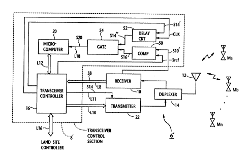
Fig. l is a block diagram schematically showing a
land site 6 which includes a known interference
detecting arrangement~ The portions of the land site 6,
which are deemed irrelevant to the instant invention, are
not shown for the sake of brevity.
In Fig. 1, a plurality of mobile units Ma-Mn are
located within a service area which is covered by the
land site 6. A receiver lO which forms part of the land
site 6 is supplied, via an antenna 12 and a duplexer 14,
with a burst signal(s) transmitted from one or more of
the mobile units Ma-Mn. The receiver 10 demodulates the
incoming burst signal and subsequently outputs a
corresponding base band signal S8. A transceiver control
section 8 includes a transceiver controller 16, a
sampling circuit 18 and a microcomputer 20. The base
band signal S8 is applied to the transceiver controller
16 via a line L8. A transmitter 22 is interconnected
between the transceiver controller 16 and the duplexer 14
via lines LlO and L12.
The sampling circuit 18 receives a signal SlO from
the receiver 10. The signal S10 is generated at an IF
(Intermediate Frequency) stage (not shown) o~ the
receiver lO and indicates electric field strength of each
of the signals in the time slots of the TDMA frame. The
sampling circuit 18 samples the signal SlO in synchronism
with a clock CLK applied thereto from the transceiver
controller 16. The clock CLK comprises a train of pulses
~ach of which is generated in synchronism with time slots
of a TDMA frame. The sampling circuit 18 applies, via a
line L14, the output thereof (~iz., sampled data) S12 to
the microcomputer 20. The microcomputer 20 includes a
ROM (not shown) for storing a program dedicated to
detecting the interference in the receive signals.
In more specific terms, the land site controller
(not shown) informs, via a line L16, the transceiver
NE-382 - 3 -
controller 16 of the overall use of the time slots of a
TDMA frame. This information which indicates the current
use of the time slots is also applied to the transmitter
22 as a signal S14 over the line L11. The transmitter 22
receives a base band signal from the transceiver
controller 16 via the line 10 and implements time slot
data transmission using the signal S14.
The microcomputer 20 receives the output signal S12
via the line L14 and also receives the information
indicating the current use of the time slots via a line
L12. This information applied to the microcomputer 20
via the line L12 corresponds to the signal S14.
Following this, the microcomputer 20 checks to see, using
the program stored in the ROM therewithin, whether or not
the output signal S12 is detected within the time slot
not in use. If this happens, interference in the data
co~~llnication channel currently used is indicated. The
microcomputer 20 advises the transceiver controller 16 of
the presence of interference. Further, the land site
controller is advise~ of the detection of interference
from the transceiver controller 16, and changes the
c~_- ~;cation channel to another one if necessary. The
manner in which the current carrier frequency is changed
to a new one is not directly concerned with the present
invention, and hence will not be discussed in detail for
the sake of brevity.
With the recent trend in high speed data
transmission in a TDMA communications system, the above-
mentioned prior art has encountered the problem in that
the detection of the interference is extremely difficult
or nearly impossible through the use of software. The
reason for this is that the speed with which the
interference detection routines can be executed are
limited and are often unable to follow the high speed
incoming data.
NE-382 - 4 -
SUMMARY OF THE INVENTION
It is an object of the present invention to
provide a hardware arrangement by which interferences in
high speed TDMA data transmission can be detected with a
simple configuration.
Another object of the present invention is to
provide a method by which interferences in high speed
TDMA data transmission can be detected without the use of
a software.
In brief, the above objects are achieved by an
arrangement and method wherein interference in a high
speed receive signal is effectively detected in a TDMA
communications system wherein a plurality of time slots
is provided within a TDMA frame. A comparator is
arranged to receive a first signal indicative of receive
signal strength and a reference level signal. The
comparator compares the magnitudes of the two signals
applied thereto and outputs a comparison result signal.
A delay circuit is supplied with a second signal
indicative of a time slot which is not in use and which
delays the second signal by a predetermined time using a
clock which is synchronized with the time slots of the
TDMA frame. A gate circuit, preceded by the comparator
and the delay circuit, is supplied with the outputs of
the comparator and the delay circuit. The gate circuit
outputs a third signal which changes a logic level in the
event that the strength of the first signal exceeds that
of the reference level signal during the time slot which
is not in use.
More specifically, a first aspect of the present
invention comes in an arrangement wherein an arrangement
for detecting an interference in a receive signal in a
time division multiple access (TDMA) c : lnications
system wherein a plurality of time slots is provided
within a TDMA frame, comprising: first means arranged to
NE-382 - 5 -
receive a first signal indicative of receive signal
strength and a reference level signal, the first means
comparing the first signal and the reference level signal
and outputting a comparison result signal; second means
which is supplied with a second signal indicative of a
time slot which is not in use and which delays the second
signal by a predetermined time using a clock which is
synchronized with the time slots of the TDMA frame; and
third means which is responsive to the outputs of the
first and second means and which outputs a third signal,
the third signal changing a logic level in the event that
the comparison result signal exists within the time slot
which is not in use.
A second aspect of the present invention comes in a
method for detecting an interference in a receive signal
in a time division multiple access (TDMA) communications
system wherein a plurality of time slots is provided
within a TDMA frame, comprising the steps of: (a)
receiving a first signal indicative of receive signal
strength and a reference level signal, and comparing the
first signal and the reference level signal and
outputting a comparison result signal, (b) receiving a
second signal indicative of a time slot which is not in
use and which delays the second signal by a predetermined
time using a clock which is synchronized with the time
slots of the TDMA frame; and (c) responding to the
ouLpuLs of the first and second means and outputting a
third signal, the third signal changing a logic level in
the event that the comparison result signal exists within
the time slot which is not in use.
BRIEF DESCRIPTION OF THE DRAWINGS
The features and advantages of the present
invention will become more clearly appreciated from the
following description taken in conjunction with the
accompanying drawings in which like elements are denoted
~-382 - 6 -
by liXe reference numerals and in which:
Fig. 1 is a block diagram showing a known
arrangement discussed in the opening paragraphs of the
instant disclosure;
Fig. 2 is a block diagram showing an embodiment of
the present invention; and
Figs. 3-4 are timing charts depicting the
operation of the present invention.
DETAILED DESCRIPTION OF THE
PREFERRED EMBODIMENTS
Reference is now made to Fig. 2, wherein an
embodiment of the present invention is schematically
illustrated in block diagram form.
The arrangement of Fig. 2 differs from that of Fig.
1 in that the former arrangement includes a transceiver
control section 8' which is configured in a different
manner as compared with the counterpart 8 of Fig. 1.
Viz., the section 8' includes a comparator 50, a delay
circuit 52 and a gate circuit 54 in lieu of the sampling
circuit 18 of Fig. 1. The remaining portions of the Fig.
2 arrangement has been described in the opening
paragraphs of the instant disclosure with reference to
Fig. 1 and as such, further descriptions thereof will be
omitted to avoid redundancy.
The comparator 50 is supplied with a reference
signal Sref and a signal S10'. The reference signal Sref
is controllable in terms of the magnitude thereof, while
the signal S10' indicates an electric field strength of
each of receive signals transmitted over a given carrier
frequency. Therefore, the signal S10' corresponds to the
signal SlO in Fig. 1. The comparator 50 compares the
signals S10' and Sref, and supplies the gate circuit 54
with an output signal 516 indicating the comparison
result. On the other hand, the delay circuit 52 receives
a clock CLK and a signal S14' both applied thereto from
NE-3~2 - 7 -
the transceiver controller 16, and delays the signal S14'
by a predetermined time using the clock CLK and
subsequently outputs a delay signal 14" which is applied
to the gate circuit 54. The clock CLK will be described
late in detail. Following this, the gate circuit 54
issues a signal S20 which indicates the presence of
interference in the receive signals as will be understood
as the description proceeds. The signal S14' corresponds
to the signal 14 applied from the transceiver controller
16 to the transmitter 22 although different notations are
given.
The operations of the Fig. 2 arrangement will be
described with reference to Figs. 3-5.
Fig. 3 illustrates timing charts (a)-(e) of: a TDMA
frame transmitted from a land site 6', a receive TDMA
frame, the clock CLK, the signal S14' applied to the
, delay circuit 52, and the output of the delay circuit 52
(viz., S14") in this order. The transmit TDMA frame as
shown includes six time slots T1-T6 in this particular
case.
It is assumed that the overall system including the
land site 6' and the mobile units Ma-Mn are controlled
such that the TDMA frame arrived at the land site 6' is
delayed by three time slots as compared with the TDMA
frame transmitted from the land site 6'. Although not
shown in Fig. 3, a guard time interval is provided
between adjacent time slots in order to absorb the
receive time differences of the signals transmitted from
the mobile units Ma-Mn located in different positions
within the service area covered by the land site 6' (Fig.
2).
As shown in the timing chart (c) of Fig. 3, the
clock CLK includes a train of pulses each of which has a
trailing edge synchronized with the termination of each
time slot. The clock CLK is generated in the
NE-382 - 8 -
transceiver controller 16. The signal S14' includes
information whether each of the six time slots is used
for communication or not. It is assumed in this
embodiment that only the time slot T2 is not used for
communication and therefore the signal 14' assumes a low
level (timing chart ~d)) during the time slot T2.
Accordingly, no signal should be received in the received
time slot T2 under normal operating conditions. In other
words, if any signal (inclusive of noise) is detected in
the received time slot T2, there is a high possibility
that the arriving signals received in the other time
slots may be contaminated.
In order to detect the interference in the received
time slot T2, the delay circuit 52 retards the time slot
usage information signal S14' by three time slots using
the clock CLK applied thereto. The timing chart of the
output of the delay circuit 52 (viz., S14") is shown in
the item (e) of Fig. 3.
The operations of the Fig. 2 embodiment will
further be discussed with Figs. 4 and 5 each of which
shows four timing charts (a)-(d).
The comparator 50 is supplied with the signal S10'
and the reference signal Sref whose level is adjustable
and previously set to an appropriate one prior to
operation. In the event that the data signals received
by the land site 6' are not subject to interference
during transmission, the signal S10' is free from noise
within the time slot T2 as shown in a timing chart (a) of
Fig. 4. The comparator 50 is arranged such that the
output thereof (vi~., S16) assumes a high level when the
reference signal Sref exceeds the signal S10'.
In this instance, the comparator 50 issues the
signal S16 which assumes a high level only during the
time slot T2 as shown in the timing chart (b) of Fig. 4.
The timing chart of the output S14" of the delay circuit
NE-382 ~ 9 ~
52 is shown in the item (c) of Fig. 4. The gate 54 takes
the form of an exclusive OR gate in this embodiment and
is supplied with the signals S16, S14" after they are
inverted. Thus, the gate 54 issues the output S20 which
assumes a high level "1" over the entire TDMA frame in
this particular instance as shown in the timing chart (d)
of Fig. 4.
On the other hand, in the event that a noise Nl
appears within the time slot T2 as shown in the timing
chart (a) of Fig. 5, the signal S16 falls to a low level
in the time slot T2 as indicated by N2. Thus, the
output S20 of the gate 54 assumes a low level "0" as
denoted by N3 within the time slot T2. Consequently, the
microcomputer 20 receives the output S20 and detects the
presence of the interference in the receive signals.
If the number of the interferences thus detected
exceeds a predetermined value within a preset time
period, the microcomputer 20 requests the land site
controller (not shown in Fig. 2), via the transceiver
controller 16, to change the carrier frequency currently
in use to another one. This operation is not directly
concerned with the present invention, and hence further
descriptions thereof will be omitted.
Although not referred to in the above, in addition
to the aforesaid channel for the TDMA frames, a control
ch~nnel may be provided for controlling calling
requests, TDMA frame timings, etc. As an alternative,
control bursts may be inserted at the leading portion of
each of the time slots T1-T6 for the same purposes.
While the foregoing description describes ona
embodiment according to the present invention, the
various alternatives and modifications possible without
departing from the scope of the present invention, which
is limited only by the appended claims, will be apparent
to those skilled in the art.