Note: Descriptions are shown in the official language in which they were submitted.
- 1 -
TITLE OF THE INVENTION
~AVEGUIDE-TYPE COUPLER/SPLITTER
BACKGROUND OF TIIE INVENTION
Field of the Invention
The present invention relates to waveguide-type
coupler/splitters effectively used in an optical fiber
communication system and optical sensor system, and
more particularly, to waveguide-type coupler/splitters
which need not be connected with any other optical
parts, such as an optical wavelength division _
multiplexer/demultiplexer, at the time of optical line
monitoring in these systems.
Description of the Prior Art
In an optical fiber communication system, such as
the one shown in Fig. 1, a signal transmitted from one
parent station 1 is divided into N number of signals
by means of a 1-input/N-output waveguide-type
coupler/splitter 2, and the individual signals are
distributed to N number of child stations 4z, ~2,
~ ~ ~ 4N by means of N number of fiber lines 3,., 32,
~ ~ ~ 3N, respectively.
Referring now to Figs. 2 to 7, 1-input/16-output
versions of the coupler/splitter 2 adapted to be used
in this system will be described by way of example.
A coupler/splitter A of the type shown in Fig. ~
uses, as each of its element coupler/splitters, a 1-
input/2-output Y-branch waveguide I in which two
output ports I~ and I~ are continuous with an 3.nput
port I~., as shown in Fig. 3. The input and output
ports Ia, I" and IQ of these individual element
coupler/splitters are concatenated to ane another in
- 2 -
four stages in a tournament-list style.
A coupler/splitter B of the type shown in Fig. 4
uses, as each of its element coupler/splitters, a 1-
input/2-output directional connector II formed of a 1-
input/2-output Y-branch waveguide and having a
junction IIu at which one of two waveguides is
continuous and the other is discontinuous, as shown in
Fig. 5. Input and output ports IIB, IIb and II~ of
these individual element coupler/splitters are
concatenated to one another in four stages.
A coupler/splitter C of the type shown in Fig. 6
uses, as each of its element coupler/splitters, a 1-
input/2-output directional coupler III formed of a 1-
input/3-output Y-branch waveguide and having a
junction IIId at which two waveguides are
discontinuous with another waveguide, as shown in Fig.
7. Input and output parts IIIa, IIIb and III of
these individual element coupler/splitters are
concatenated to one another in four stages.
In monitoring the optical fiber lines 3a, 32,
~ ~ ~ 3N without interrupting communication between
the parent station and the child stations 4,., 42,
~ ~ ~ 4~, in the optical communication system shown
in Fig. 1, it is necessary to connect an optical line
monitoring device (e. g., OTDR) 5, which uses light
with a monitoring wavelength ~.Z different from a
communication wavelength ~.z, as shown in Fig. 8, to
the arrowed spat (Fig. 1) of an optical path
connecting the parent station 1 and the 1-input/N=
output coupler/splitter 2, through an optical
wavelength division multiplexer/demultiplexer 6 for
synthesizing and dividing light waves with the
CA 02058309 2001-05-16
72465-34
3
wavelengths ~,1 and
Thus, when using the 1-input/N-output
coupler/split.ter 2 composed of the concatenated 1-input/2-
output element coupler/:~plitters I, II or III of the
conventional configuration described above, the interposition
of another optical part, such as the optical wavelength
division mulitiplexer/demultiplexer (~,1 # ~,2) or an optical
coupler (~,1 = ~,z) , is required in connecting the optical line
monitoring device 5 between the coupler/splitter 2 and the
parent station 1.
OBJECT AND SUMMARY OF THE INVENTION
The object of the present invention is to provide a
waveguide-type coupler/:~plitter capable of optical line
monitoring without the .interposition of any other optical part,
such as an optical wavelength division
multiplexer/demultiplexE=r or optical coupler.
In order to achieve the above object, according to
the present invention, there is provided a waveguide-type
coupler/splitter compri:~:ing: a plurality of element
coupler/splitters concatenated to one another, input ports of
said individual element coupler/splitters being connected to
output ports of other element coupler/splitters, said element
coupler/splitter in a f_L_rst stage being a 2-input/2-output
coupler/splitter, where_Ln said element coupler/splitter in the
first stage has a branch coupling ratio which is wavelength-
independent for light ha,;ring a wavelength falling within a
predetermined range, anc~ each of said element coupler/splitters
in a second stage and in subsequent stages being a 1-input/2-
output coupler/splitter.
CA 02058309 2001-05-16
72465-34
3a
In the couple:r/splitter of the present invention, the
first-stage element coupler/splitter is a 2-input/2-output
coupler/splitter, and therefore, the
input ports thereof can be used separately, one for
communication and the other for optical line
monitoring. Alternatively, the two input ports may be
used individually as a running version and as a stand-
by (spare).
BRIEF DESCRIPTION OF THE DRAWINGS
Fig. 1 is a schematic view showing an example of
an optical fiber communication system;
Fig. 2 is a schematic view showing an example of -
a conventional waveguide-type coupler/splitter;
Fig. 3 is a schematic view showing a 1-input/2-
output element coupler/splitter of the Y-branch
waveguide type used in the coupler/splitter of Fig. 2;
Fig. 4 is a schematic view showing another
example of the conventional waveguide-type
coupler/splitter;
Fig. 5 is a schematic view showing a 1-input/2-
output element coupler/splitter of the directional
connector type used in the coupler/splitter of Fig. 4;
Fig. 6 is a schematic view showing still another
example of the conventional waveguide-type
coupler/splitter;
Fig: 7 is a schematic view showing a 1-input/2-
output element coupler/splitter of the directional
connector type used in the coupler/splitter of Fig. 6;
Fig. 8 is a schematic view showing an optical
part interposed for optical line monitoring in the
optical communication system of Fig. 1;
Fig. 9 is a schematic view showing a 2-input/16-
output waveguide-type coupler/splitter according to
the present invention; and
- 5 -
Fig. 10 is a schematic view showing a 2-input/2-
output element coupler/splitter of the directional
connector type arranged in a .first stage of the
coupler/splitter of the present invention.
DETAILED DESCRIPTION OF TfIE PREFERRED EMBODIMENTS
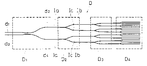
Fig. 9 is a schematic view showing a 2-input/16-
output coupler/splitter. In this coupler/splitter D,
a First-stage element coupler/splitter D~ is a 2-
input/2-output coupler/splitter, as shown in Fig. 10.
The input port Ia of the Y-branch waveguide I shown in
Fig. 3 is concatenated to each of output ports dz and
d4 of the coupler/splitter D,., thus forming a second-
stage element coupler/splitter group D2 having four
output ports. Further, the input port Ia of the Y-
branch waveguide I is concatenated to each of the
output ports Ib and I~ of each group-DZ Y-branch
waveguide, thus forming a third-stage element
coupler/splitter group D3 having eight output ports.
Likewise, the input port Ia of the Y-branch waveguide
I is concatenated to each of the output ports Ib and
I~ of each group-group D3 Y-branch waveguide, thus
forming a fourth-stage element coupler/splitter group
D4 having sixteen output ports.
After the formation of the group D4, additional
Y-branch waveguides are successively concatenated in
the same manner as aforesa9.d. If the 1-input/2-output
element coupler/splitters are connected in _~n - 1)
stages in all, the resulting coupler/splitter becomes
a ~-input/2n-output coupler/splitter.
The element coupler/splitters concatenated in the
second stage and its subsequent stages are not limited
CA 02058309 2001-05-16
72465-34
6
to the Y-branch waveguide I shown in Fig. 3, and may be of the
type II shown in Fig. 5 or the type III shown in Fig. 7 or
suitable combinations o:E these types I, II and III.
In the wavegu:ide-type coupler/splitter according to
the present invention, i~:he coupler/splitter D1 as an element
coupler/split.ter in the first stage is arranged so that a
signal with a communical_ion wavelength ~,1 is inputted through
the one input. port dl (or: d2), while a light beam for optical
line monitoring with a monitoring wavelength ~,2 is inputted
1G through the other input fort d2 (or dl).
Preferably, the coupler/splitter D1 should be one
whose branch coupling r<~tio for light having a wavelength
intermediate between the communication wavelength ~,1 and the
monitoring wavelength ~,~;is wavelength-independent, that is, a
l~ coupler/split.ter which :i;s wavelength-flattened between the
communication and monitoring wavelengths.
As an example of the coupler/splitter of this type,
there is an asymmetric Mach-Zehnder interferometer-type optical
waveguide coupler with wavelength insensitive coupling ratio by
2C KANAME JINGUJI, et al ":I:ntegrated Photonics Research" 1990
Technical Digest Series Volume 5 Conference Edition March 26 to
28 1990, Hilton Head, North Carolina (WINO) Topical Meeting on
Integrated Photonic Research.
Preferably, the coupler/splitter D1 is arranged so
2~~ that a slit i.s cut in the one input port dl, for example, and a
filter which transmits :Light with the communication wavelength
1 and reflects light wi.t:h the monitoring wavelength ~,2 is
housed in the slit, and ,at the same time, another slit is cut
CA 02058309 2001-05-16
72465-34
6a
in the other input port~~ d2, and a filter which reflects light
with the communication wavelength ~1 and transmits light with
the monitoring wavelength ~
2(~~83~~
Thus, according to the present waveguide-type
coupler/splitter, the element coupler/splitters used
are equal in number to the ones used in the
conventional coupler/splitter. Since the first-stage
element coupler/splitter is a 2-input/2-output
coupler/splitter, however, one of its input ports can
be used for optical line monitoring, so that it is
unnecessary to use an exclusive optical part for
optical line monitoring which conventionally is
essential.