Note: Descriptions are shown in the official language in which they were submitted.
2 0 5 8 ~
The present invention relates to a discharge
excitation gas laser device used in the industrial field.
In recent years attention has been paid to excimer
lasers as new laser light sources for industrial use. An
excimer laser is one of ultraviolet lasers, by which
oscillation lines can be obtained at wavelengths from 353 nm
to 193 nm by combining a rare gas such as krypton, xenon,
etc. with a halogen gas such as fluorine, chlorine, etc. for
a laser medium gas. Since it is possible to obtain a high
output for a short wavelength region by using an excimer
laser with respect to a conventional laser device, it is
expected to be used as a new light source in various fields
such as industry, medical service, etc. In particular, in
steps of fabricating semiconductor devices, demand therefore
is rising rapidly to serve as a light source for replacing
mercury lamps in fabricating super LSIs. Excimer laser
devices can be classified, depending on the method for
exciting the laser medium gas, into discharge excitating
type, electron beam excitation type, X-ray excitation type,
microwave excitation type, etc. Among them, discharge
excitation type excimer laser devices are used often in the
industrial field due to the fact that the construction
thereof is simple, that a high repetition
20584~
1 rate is possible and that the size thereof can be easily
reduced.
Hereinbelow a prior art discharge excitation
gas laser device will be explained.
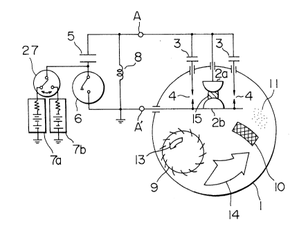
Fig. 15 is a diagram indicating schematically
the construction of a prior art discharge excitation high
repetition rate excimer laser device. In Fig. 15,
reference numeral 1 is a gas-tight vessel; 2a and 2b are
a pair of main electrodes; 3 is a peaking condenser; 4 is
a preionization gas; 9 is a ventilation fan; and 10 is a
heat exchanger, these constituting a laser oscillation
tube. Laser medium gas 11 is enclosed in the gas-tight
vessel 1. A secondary circuit composed of the peaking
condenser 3, the preionization gap 4 and the main
electrodes 2a, 2b is connected with a primary circuit
composed of a switch 6 consisting of a thyratron, etc., a
charging condenser 5, a charging inductor 8 and a DC high
voltage power supply 7 at points A and A'. 12 is an
arrow indicating transfer current; 13 is an arrow
indicating the direction of rotation of the ventilation
fan 9; 14 is an arrow indicating gas flow generated by
the ventilation fan 9; and 15 shows a discharge region.
Now the operation of the discharge excitation
high repetition rate excimer laser device constructed as
described above will be explained. At first, electric
charge is stored in the charging condenser 5 by the DC
high voltage power supply 7. The switch 6 is closed at a
point of time where a predetermined amount of electric
-- 2
205840~
1 charge is stored in the charging condenser 5 and the
potential difference between the two terminals thereof
arrives at a certain value. When the switch 6 is closed,
the potential at the point A increases in the negative
direction with respect to the potential at the point A'.
As the potential at the point A increases in the negative
direction, dielectric breakdown is produced at the pre-
ionization gas 4. In this way preionization is produced
between one of the main electrodes 2a and the other main
electrode 2b. At the same time the transfer current 12
flows in the direction indicated by the arrow from the
charging condenser 5 and electric charge is transferred
to the peaking condenser 3. As electric charge is
transferred to the peaking condenser 3, the potential
difference between the main electrodes 2a and 2b
increases. When it arrives at the discharge starting
voltage, a DC pulse discharge is generated between the
one main electrode 2a and the other main electrode 2b.
Thus electric energy transferred to the peaking condenser
3 is injected in the discharge region 15. In this way
the laser medium gas 11 in the discharge region 15 is
excited in a high energy state by this DC pulse discharge
so that a so-called inverted distribution is established.
Energy thus stored in the laser medium gas 11 is output-
ted in the form of a laser beam by an optical resonator(not shown in the figure). In order to have a sustained
laser beam suitable for a purpose of working, etc., a
series of the operations described above may be effected
205840~
with a high repetition rate.
However, since the laser medium gas 11 in the
discharge region 15 is deteriorated gradually by the laser
exciting discharge and thus discharge characteristics are
worsened, the succeeding DC pulse discharge is unstable and
proper laser output cannot be obtained, until the laser
medium gas 11 between the main electrodes 2a and 2b is
replaced by fresh gas by diffusion.
Consequently the ventilation fan 9 and the heat
exchanger 10 are disposed in the gas-tight vessel 1 in the
prior art device so as to form the gas flow 14 in the gas-
tight vessel 1 by rotating the ventilation fan 9 in the
direction of rotation 13 indicated by the arrow. The laser
oscillation is produced with a high repetition rate, in order
to take out a sustained laser beam, by replacing the laser
medium gas 11 between the one main electrode 2a and the other
main electrode 2b by fresh gas and by cooling and
regenerating it.
However, the prior art construction described above
has a problem that boundary layers are formed in the
neighborhood of the surfaces of the one main electrode 2a and
the other main electrode 2b and thus a satisfactory flow
speed can not be secured, even if the flow speed of the laser
medium gas 11 between the main electrodes 2a and 2b in Fig.
15 is increased.
Fig. 16 is a schematical diagram for explaining
the formation of the boundary layers. In Fig. 16,
hatched regions represent the boundary layers
-- 4
2058402
1 16. Further Fig. 17 is a graph indicating an example of
the distribution of the flow speed on a transversal
cross-section of Fig. 16 along a line indicated by B-B'.
As indicated in Fig. 17, the flow speed is lower in the
neighborhood of the surfaces of the one main electrode 2a
and the other main electrode 2b than in the central
portion. Because of this phenomenon, among positive and
negative ions generated by the laser excitation discharge
positive ions are attracted by the cathode, while nega-
tive ions are attracted by the anode. That is, since theboundary layers 16 are formed in the neighborhood of the
surfaces of the one main electrode 2a and the other main
electrode 2b and the flow speed is low there, when the
repetition frequency is high, the succeeding laser
excitation discharge is started, before the laser medium
gas 11 in the neighborhood of the surfaces of the one
main electrode 2a and the other main electrode 2b is
replaced completely by fresh gas. Therefore atoms, which
are apt to be positively ionized, are distributed with a
relatively high concentration in the neighborhood of the
cathode, while atoms, which are apt to be negatively
ionized, are distributed similarly in the neighborhood of
the anode. Now this phenomenon is considered, taking a
kripton fluoride (KrF) excimer laser as an example. Rare
gas such as kripton, helium, etc., which is apt to be
ionized positively, is distributed so as to have a great
concentration gradient in the neighborhood of the
cathode, i.e. the main electrode 2b, while fluorine,
205840
which is apt to be ionized negatively, is distributed
similarly in the neighborhood of the anode, i.e. the main
electrode 2a. As a result, the laser medium gas 11
between the main electrodes 2a and 2b is no longer uniform
and the uniformity of the laser excitation discharge is
impaired. Therefore the excitation efficiency is lowered and
the pulse energy of the laser beam is decreased. This means
that at a high repetition rate oscillation the energy
injected in the discharge region 15 should be increased, if
it is desired to have the same pulse energy. However, when
the energy density injected in the discharge region 15 is
increased, deterioration of the laser medium gas 11 is
remarkably accelerated. Further, for a discharge excitation
high repetition rate excimer laser, stable glow discharge by
DC pulse discharge is inevitable and such a high energy
discharge causes ion bombardment on the one main electrode 2a
and the other main electrode 2b. As described above, in a
KrF laser there exist at a relatively high concentration of
fluorine in the neighborhood of the surface of the one main
electrode 2a serving as the anode and rare gas such as
krypton, etc. in the neighborhood of the other main electrode
2b serving as the cathode. Consequently, when laser
excitation discharge is generated, a number of fluorine ions
collide with the anode 2a. Since fluorine is extremely
reactive, in a state where fluorine ions are implanted in the
one main electrode 2a, they react with metal constituting the
-- 6
d
2 0 S 8 4 5 ~
surface of the electrode, e.g. nickel, which produces metal
fluoride such as nickel fluoride, etc. The surface of the
one main electrode 2a is locally protruded convexly by this
metal fluoride. On the other hand, although rare gas
colliding with the other main electrode 2b is scarcely
reactive, since it sputters the surface of the electrode even
at a kinetic energy as low as the laser excitation discharge
energy, the surface of the other main electrode becomes
concave. If the surfaces of the one main electrode 2a and
the other main electrode 2b are locally deformed, the
uniformity of the electric field is disturbed, which causes
local concentration of the discharge. For this reason, not
only the spatial uniformity of the laser beam is worsened,
but also the life of the main electrodes 2a and 2b is
remarkably shortened.
Consequently, in conventional devices, in order to
be able to produce a high repetition rate oscillation, a
measure is taken, by which the laser medium gas ll is
circulated with an extremely high speed. However, since
influences of the boundary layers increase more and more so
that they cannot be neglected, as the flow speed of the laser
medium gas 11 increases, the necessary flow speed increase
exponentially with increasing repetition frequency. As the
result, the size of the ventilation fan 9 has to increase so
that it occupies the major part of the laser device both
spatially and for electric power consumption.
-- 7
205840~
The present invention has been developed in order
to solve the problem described above of the prior art
technique and an object thereof is to provide a discharge
excitation gas laser device, which has excellent output
stability, even at a high repetition rate oscillation, and
has a high efficiency, a long life, a small size and a small
weight.
In order to achieve this object, the discharge
excitation gas laser device according to the present
invention is provided with a laser medium and a pair of
electrodes in a gas-tight vessel and has a construction in
which the polarity of the DC pulse applied to the pair of
electrodes is inverted to excite the laser medium by
discharge.
Owing to this construction, the distribution of
atoms and ions constituting the laser medium in the discharge
region, including the neighborhood of the main electrodes, is
made uniform even at the high repetition rate oscillation.
Consequently, without unnecessarily increasing the flow speed
of the laser medium gas, the stability of the DC pulse
discharge at the high repetition rate oscillation is
improved, reduction in the pulse energy is avoided because of
a high efficiency operation, and the life of the laser medium
gas is elongated. Further, since unequal impairment of the
main electrodes is removed, the life of the whole device is
elongated. Furthermore, since a small size ventilation
-- 8
205840~
device is sufficient for circulating the laser medium gas, it
is possible to realize a discharge excitation gas laser,
which is not only small and light but also of small electric
power consumption.
The invention will be described in more detail by
reference to the accompanying drawings, in which:
Fig. 1 is a diagram indicating schematically the
construction of a discharge excitation high repetition rate
excimer laser device used in a first embodiment of the
present invention;
Fig. 2 is a circuit diagram of the principal part
of the excimer laser device of Fig. 1 using a directional
switch;
Fig. 3 is a diagram indicating schematically the
construction of a discharge excitation high repetition rate
excimer laser device used in a second embodiment of the
present invention;
Fig. 4 is a diagram indicating schematically the
construction of a discharge excitation high repetition rate
excimer laser device used in a third embodiment of the
present invention;
Fig. 5 is a diagram indicating schematically the
construction of a discharge excitation high repetition rate
excimer laser device used in a fourth embodiment of the
present invention;
_ g
205840~
Fig. 6 is a circuit diagram of the principal part
of the excimer laser device of Fig. 5;
Fig. 7 is an equivalent circuit diagram in a cycle
L of the excimer laser device of Fig. 5;
Fig. 8 is an equivalent circuit diagram in a cycle
(L+l) of the excimer laser device of Fig. 5;
Fig. 9 is a circuit diagram of a discharge
excitation high repetition rate excimer laser device used in
a fifth embodiment of the present invention;
Fig. 10 is a circuit diagram of a discharge
excitation high repetition rate excimer laser device used in
a sixth embodiment of the present invention;
Fig. 11 is a circuit diagram of a discharge
excitation high repetition rate excimer laser device used in
a seventh embodiment of the present invention;
Fig. 12 shows a B-H curve for a saturable magnetic
core;
Fig. 13 is a diagram indicating schematically the
construction of a discharge excitation high repetition rate
excimer laser device used in an eighth embodiment of the
present invention;
Fig. 14 shows an output waveform of a bias circuit
used in the excimer laser device of Fig. 13;
Fig. 15 is a diagram indicating schematically the
construction of a prior art discharge excitation high
repetition rate excimer laser device;
-- 10 --
205840~
Fig. 16 is a schematic diagram for explaining the
formation of boundary layers in the prior art of Fig. 15; and
Fig. 17 shows a curve representing an example of
the flow speed distribution on a transversal cross-section
along a line B-B' in Fig. 16.
Fig. 1 is a diagram indicating schematically the
construction of a discharge excitation high repetition rate
excimer laser device used in the first embodiment of the
present invention. In Fig. 1, the parts corresponding to the
constituent elements in the prior art example indicated in
Fig. 15 are indicated by the same reference numerals and
explanation thereof will be omitted and only the parts, which
are features of the present embodiment, will be explained.
In Fig. 1, reference numeral 7a is a positive high voltage
power supply; 7b is a negative high voltage power supply; and
27 is a high voltage switch switching-over the DC high
voltage power supplies 7a and 7b. Further a series of
operations from a step in which the charging condenser 5 is
charged with electric charge up to a step just before the
charging condenser 5 is charged again with electric charge,
after the charge has been consumed by the laser oscillation,
is called one cycle.
At first, it is supposed that the high voltage
switch 27 is connected with the side of the positive DC high
voltage power supply 7a in a certain cycle J. At this time,
the electrical operation of the discharge excitation high
-- 11 --
~ = ~Y
2058402
repetition rate excimer laser device in the present
embodiment is identical to the operation of the prior art
example indicated in Fig. 15. That is, when the switch 6 is
closed at the point of time where the charging of the
charging condenser 5 has been terminated, electric charge is
transferred from the charging condenser 5 to the peaking
condenser 3. Together therewith, the potential at the point
A increases in the negative direction with respect to the
potential at the point A'. Finally a DC pulse discharge is
produced, for which the one main electrode 2a serves as the
cathode, while the other main electrode 2b serves as the
anode. The laser medium gas 11 in the discharge region 15 is
discharge-excited, which gives rise to the laser oscillation.
In the succeeding cycle (J+l) the high voltage
switch 27 is switched-over to the side of the negative DC
high voltage power supply 7b. Consequently, in this cycle
(J+1), the charging condenser 5 is negatively charged with
respect to the potential at the point A'. When the switch-6
is closed at the point of time where the charging of the
charging condenser 5 has been terminated, electric charge is
transferred from the charging condenser 5 to the peaking
condenser 3. Together therewith, the potential at the point
A increases in the positive direction with respect to the
potential at the point A'. Finally a DC pulse discharge is
produced, for which the one main electrode 2a serves as the
anode, while the other main electrode 2b serves as the
- 12 -
2058402
cathode. The laser medium gas 11 in the discharge region 15is discharge-excited, which gives rise to the laser
oscillation.
As described above, in the first embodiment, the
polarity of the one main electrode 2a and the other main
electrode 2b is inverted alternately for every cycle to give
rise to oscillations. This is further considered taking a
KrF excimer laser as an example. In the cycle J rare gas
atoms such as krypton, which are apt to be positively
ionized, Are attracted to the neighborhood of the surface of
the one main electrode 2a. On the contrary, in the
succeeding cycle (J+l), since the main electrode 2a acts as
the anode, fluorine atoms, which are apt to be negatively
ionized, are attracted and the rare gas atoms are repulsed.
On the other hand, a process, which is inverse to the process
in the neighborhood of the surface of the one main electrode
2a, takes place in the neighborhood of the surface of the
other main electrode 2b. Since the operations described
above are repeated alternatively, the distribution of atoms
and ions constituting the laser medium gas 11 in the
discharge region 15 including the neighborhood of the pair of
main electrodes 2a and 2b becomes uniform.
As a result, the laser medium gas 11 in the
discharge region 15 can be completely replaced by fresh gas
without using a flow speed of the laser medium gas 11 which
is as high as that used in the conventional high repetition
- 13 -
",
205840~
rate excimer laser device. Therefore the DC pulse dischargeis stable and the output of the laser beam does not decrease
even at high repetition rate oscillation. This means that a
small quantity of energy necessary for obtaining the same
laser beam output may be sufficient. Since it is possible to
suppress deterioration of the laser medium gas 11, due to the
fact that surplus energy is emitted to the discharge region
15, to the minimum value, remarkable improvement can be
obtained both on the efficiency and on the deterioration of
the laser medium gas 11. In addition, since the polarity of
the main electrodes 2a and 2b is inverted for every cycle,
the deterioration of the surfaces of the main electrodes due
to ion bombardment is equal to each other for the main
electrodes 2a and 2b. In this way, since local concentration
of the discharge is alleviated, not only the spatial
uniformity of the output laser beam is improved, but also the
life of the main electrodes is remarkably elongated.
Furthermore, since the flow speed of the laser
medium gas 11 is not necessarily as high as that used in the
conventional device, it is possible to reduce the
size of the ventilation fan 9 and the amount of electric
power for driving it. Thus, it is also possible for the
whole device to realize a discharge excitation high
repetition rate excimer laser device having a small size and
a small electric power consumption.
- 14 -
2053~0 ~
A bidirectional switch (e.g. spark gap) is required
for the switch 6 in Fig. 1. Now an embodiment in which uni-
directional switches such as, e.g. thyratrons, are used will
be explained. In Fig. 2 the arrows indicated in the switches
6a and 6b show switching current flow directions. The
switches 6a and 6b are connected in parallel with polarities
inverted to each other. When the high voltage switch 27 is
connected with the positive DC high voltage power supply 7a,
only the switch 6a is triggered and on the contrary when the
high voltage switch 27 is connected with the negative DC high
voltage power supply 7b, only the switch 6b is triggered.
Fig. 3 is a diagram indicating schematically the
construction of a discharge excitation high repetition rate
excimer laser device used in the second embodiment of the
present invention. In this embodiment the positive and
negative DC high voltage power supplies 7a and 7b are not
switched-over alternately for every cycle by means of the
high voltage switch 27 as in the first embodiment indicated
in Fig. 1, but one DC high voltage power supply 7 outputs a
positive and a negative DC high voltage alternately for every
cycle. Otherwise the operation and the effect thereof are
identical to those described for the first embodiment
indicated in Fig. 1.
Fig. 4 is a diagram indicating schematically the
construction of a discharge excitation high repetition rate
excimer laser device used in the third embodiment of the
- 15 -
205~ 02
present invention. In this embodiment the laser device isprovided with 2 routes composed of a charging condenser 5a
and a switch 6a, and a charging condenser 5b and a switch 6b,
respectively. These two series connections are connected in
parallel so as to be in directions opposite to each other.
The DC high voltage power supply 7 is connected with points
Ca and Cb, indicated in Fig. 4, and switched-over for every
cycle by means of the high voltage switch 27. Further the
center point of the charging inductor 8 is grounded.
Otherwise this embodiment is identical in its construction to
the first embodiment indicated in Fig. 1 or the second
embodiment indicated in Fig. 2.
Now the operation of the discharge excitation high
repetition rate excimer laser device of the third embodiment
indicated in Fig. 4 will be described. At first, it is
supposed that in a certain cycle K the high voltage switch 27
is connected with the point Ca, i.e. the side of the charging
condenser 5a. At this time, the electrical operation of the
discharge excitation high repetition rate excimer laser
device in the present embodiment is identical to the
operation of the conventional example indicated in Fig. 15.
That is, when the switch 6a is closed at the point of time
where the charging of the charging condenser 5a has been
terminated, electric charge is transferred from the charging
condenser 5a to the peaking condenser 3. Together therewith,
the potential at the point A increases in the negative
- 16 -
2058~ 0~
direction with respect to the potential at the point A'.-Finally a DC pulse discharge is produced, for which the one
main electrode 2a serves as the cathode, while the other main
electrode 2b serves as the anode. The laser medium gas 11 in
the discharge region 15 is discharge-excited, which gives
rise to the laser oscillation.
In the succeeding cycle (K+l) the high voltage
switch 27 is switched-over to the point ~b, i.e. the side of
the charging condenser 5b. When the switch 6b is closed at
the point of time where the charging of the charging
condenser 5b has been terminated, electric charge is
transferred from the charging condenser 5b to the peaking
condenser 3. Together therewith, inversely to the direction
in the cycle K, the potential at the point A increases in the
positive direction with respect to the potential at the point
A'. Finally a DC pulse discharge is produced, for which the
one main electrode 2a serves as the anode, while the other
main electrode 2b serves as the cathode. The laser medium
gas 11 in the discharge region 15 is discharge-excited, which
gives rise to the laser oscillation.
As described above, in the third embodiment,
although the DC high voltage power supply 7 is uni-polar, the
oscillation is repeated by inverting the polarity of the one
main electrode 2a and the other main electrode 2b alternately
for every cycle in the same way and the effect thus obtained
- 17 -
2058402
is identical to that obtained in the first and the second
embodiment.
Fig. 5 is a diagram indicating schematically the
construction of a discharge excitation high repetition rate
excimer laser device used in the fourth embodiment of the
present invention. In Fig. 5, 17a, 17b, 18a and 18b are
switches constituting a switching circuit. Fig. 6 is a
circuit diagram of the principal part for explaining the
- 17a -
2058402
1 operation of the discharge excitation high repetition
rate excimer laser device indicated in Fig. 5. In Fig.
6, points X and X' are confluence or ramification points
of the transfer current 12 flowing in directions
indicated by different arrows.
Now the operation of the discharge excitation
high repetition rate excimer laser device in the fourth
embodiment indicated in Fig. ~ will be explained. It is
supposed that the switches are so set that the switches
17a and 17b are turned-on, while the switches 18a and 18b
are turned-off in a certain cycle L. At first, electric
charge is stored in the charging condenser 5 by the DC
high voltage power supply 7. During this charging period
of the charging condenser 5, on and off setting of the
switches 17a, 17b, 18a and 18b is effected. Up to the
point of time where the switch 6 is closed, since the
potential difference between the two terminals of the
charging inductor 8 is almost zero, it is not necessary
for the switches 17a, 17b, 18a and 18b to switch the high
voltage. At this time, the circuit of the discharge
excitation high repetition rate excimer laser device in
the fourth embodiment is equivalent to the circuit
indicated in Fig. 7. Consequently the electrical opera-
tion in this cycle L is identical to the operation of the
prior art discharge excitation high repetition rate
excimer laser device indicated in Fig. 15. When the
switch 6 is closed at the point of time where the charg-
ing of the charging condenser 5 has been terminated, the
- 18 -
2058~ 0~
transfer current 12 flows from the charging condenser 5 to
the peaking condenser 3. The transfer current 12 flows out
from the point A to the point A' as indicated by the arrows.
Electric charge is transferred to the peaking condenser 3 by
this transfer current 12. Together therewith, the potential
at the point A increases in the negative direction with
respect to the potential at the point A'. Finally a DC pulse
discharge is produced, for which the one main electrode 2a
serves as the anode, while the other main electrode 2b serves
as the cathode. The laser medium gas 11 in the discharge
region 15 is discharge-excited, which gives rise to the laser
oscillation.
In the succeeding cycle (L+1) the switches
indicated in Fig. 6 are so set that the switches 18a and 18b
are turned-on, while the switches 17a and 17b are turned-off.
Also in this cycle (L+l), similarly to the cycle L, since the
on and off setting of the switches 17a, 17b, 18a and 18b is
effected during the charging period of the charging condenser
5, it is not necessary for the switches 17a, 17b, 18a and 18b
to switch-over the high voltage. At this time, the circuit
of the present embodiment is equivalent to the circuit
diagram indicated in Fig. 8. When the switch 6 is closed at
the point of time where the charging of the charging
condenser 5 has been terminated, the charge-transfer current
12 flows from the charging condenser 5 to the peaking
condenser 3, the direction of the current being from the
-- 19 --
2058~ 02
point A' to the point A, as indicated by the arrows.
Consequently, in this cycle (L+l), electric charge is
transferred to the peaking condenser 3 by the transfer
current 12. Together therewith, contrary to the cycle L, the
potential at the point A' increases in the negative direction
with respect to the potential at the point A. Finally a DC
pulse discharge is produced, for which the one main electrode
2a serves as the anode, while the other main electrode 2b
serves as the cathode. The laser medium gas 11 in the
discharge region 15 is discharge-excited, which gives rise to
the laser oscillation.
As described above, in the fourth embodiment, the
oscillation is repeated by inverting the polarity of the one
main electrode 2a and the other main electrode 2b alternately
for every cycle by means of the switching circuit composed of
a plurality of switches 17a, 17b, 18a and 18b and it is equal
in effect to the first and the third embodiments. Further,
since the switches 17a, 17b, 18a and 18b are switched-over in
a state where no high voltage is applied thereto and they do
not switch any high voltage as the switch 6, almost no
switching loss in the switches 17a, 17b, 18a and 18b is
produced. Consequently, increase in the loss due to the fact
that the switching circuit is additionally mounted on the
prior art discharge excitation high repetition rate excimer
laser device can be practically neglected. For the switches
17a, 17b, 18a and 18b constituting the switching
- 20 -
. 1
2058402
circuit, e.g. high voltage relays, semiconductors, etc. canbe used.
Fig. 9 is a circuit diagram of a discharge
excitation high repetition rate excimer laser device used in
the fifth embodiment of the present invention. In this
embodiment, the switches 17a, 17b, 18a and 18b of the fourth
embodiment constituting the switching circuit are constructed
by using thyristors 41a, 41b, 42a and 42b, which are semi-
conductor switches. Otherwise it is identical in operation
and effect to the fourth embodiment indicated in Fig. 6.
Triggering circuits for the thyristors 41a, 41b, 42a and 42b
are omitted, because they have no direct relation with the
present invention. In the present embodiment, it corresponds
to turning-on the switches to input trigger signals to the
lS gates of the thyristors 41a, 41b, 42a and 42b, while it
corresponds to turning them off to input no trigger signals
thereto. Since the setting of these thyristors 41a, 41b, 42a
and 42b is effected during the charging period (usually
several ms) of the charging condenser 5, the switching speed
thereof may not be very high and therefore it is not
necessary to use any high speed thyristors, which are
expensive. In the present embodiment only the withstand
voltage and the current capacity of the thyristors 4la, 4lb,
42a and 42b should be taken into account. If one element
cannot fulfil these requirements, a plurality of elements
connected suitably in series and/or in parallel can be used
- 21 -
2058402
therefor. Further, although the present embodiment has beenexplained, supposing that thyristors are used for example for
semiconductor switches, the same operation and effect can be
expected also for other semiconductor elements such as
transistors, FETs, etc., if the withstand voltage and the
current capacity thereof fulfil the noted requirements.
Fig. 10 is a circuit diagram of a discharge
excitation high repetition rate excimer laser device used in
the sixth embodiment of the present invention. In this
embodiment, the switches 17a, 17b, 18a and 18b for
constituting the switching circuit indicated in Fig. 6 are
replaced by tetrode thyratrons 43a, 43b, 44a and 44b, which
are discharge switches. Otherwise this embodiment is
identical in operation and effect to the fourth embodiment
indicated in Fig. 6. 45a, 45b, 46a and 46b are control grids
of the tetrode thyratrons 43a, 43b, 44a and 44b,
respectively. Since heating circuits and trigger circuits
for the tetrode thyratrons 43a, 43b, 44a and 44b have no
direct relation with the present invention, they are omitted.
For the tetrode thyratrons, it corresponds to switching-off
to bias the control grids 45a, 45b, 46a and 46b negatively
with respect to the respective cathodes, while it corresponds
to switching-on to remove the negative biases. The peak
value of the laser excitation discharge voltage in the
discharge excitation high repetition rate excimer laser is
usually over 20 kV, although it is transient. Therefore it
- 22 -
~:;
r
235~40.
is required that the withstand voltage of the switches 17a,
17b, 18a and 18b indicated in Figs. 5 and 6 is over 20 kV.
That is, if semiconductor switches are used therefor, it is
necessary to use a plurality of semiconductor switches having
a withstand voltage of several kV per one switch connected in
series in multistage. However, if discharge switches such as
thyratrons are used, since it is possible to easily realize a
withstand voltage higher than 40 kV by one stage, the
construction of the whole device is simplified and
reliability is improved. Although explanation of the present
invention has been made, taking tetrode thyratrons as an
example, it is a matter of course that the same operation and
effect can be expected also for discharge switches such as
spark gaps, if the withstand voltage and the current capacity
thereof fulfil the noted requirements.
Fig. 11 is a circuit diagram of a discharge
excitation high repetition rate excimer laser device in the
seventh embodiment of the present invention. In this
embodiment, saturable reactors are used in place of the
switches 17a, 17b, 18a and 18b for constructing the switching
circuit indicated in Fig. 6. The elements corresponding to
the constituent elements in the fourth embodiment indicated
in Fig. 5 or 6 are indicated by the same reference numerals.
In Fig. 11, l9a, l9b, 20a and 20b represent saturable
reactors corresponding to the switches 17a, 17b, 18a and 18b,
respectively, in the fourth embodiment indicated in Fig. 6.
- 23 -
205~4~
Further 21a, 21b, 22a and 22b are bias circuits, which make
excitation current flow through the saturable reactors l9a,
l9b, 2Oa and 2Ob, respectively. In the seventh embodiment,
since the saturable reactors l9a, l9b, 20a and 20b play also
the role of the charging inductor in common, the charging
inductor 8, which was necessary for the first to sixth
embodiments of the present invention, can be omitted. The
forward direction is taken as the direction in which the
charge-transfer current 12 indicated by the arrows flows
through the respective saturable reactors l9a, l9b, 2Oa and
20b. In the case of not such a charge-transfer current 12
but of the excitation current, it is also taken as a forward
current when the direction of the magnetic field induced by
the excitation current in the related saturable magnetic core
is in accordance with the direction of the magnetic field
induced by the charge-transfer current 12 in the same
saturable magnetic core.
The direction opposite to the forward direction is
called "reverse direction". In the case of not such a
transfer current 12, but of the excitation current, it is
also taken as a reverse current, when the direction of the
magnetic field induced by the excitation current in the
related saturable magnetic core is opposite to the direction
of the magnetic field induced by the transfer current 12 in
the same saturable magnetic core.
Fig. 12 is a conceptual diagram of a B-H curve for
a saturable magnetic core material used for the saturable
- 24 -
, f, . r
~`
20584~
reactors, e.g. a soft magnetic material such as amorphous
magnetic material, etc., for explaining the state described
above. In Fig. 12, a curve 31 indicated by a broken line is
a DC magnetization curve for the saturable magnetic core
material, while a curve 32 indicated by a full line
represents a magnetization curve in a real working frequency
band of the transfer current 12. Further the forward
saturation magnetic flux density is denoted by +Bs, while the
reverse saturation magnetic flux density is denoted by -Bs,
which are indicated in Fig. 12.
Now the operation of the seventh embodiment will be
explained, referring to Figs. 11 and 12. At first, in a
certain cycle M, the saturable reactors l9a and l9b are
excited in the forward saturated state or a state close
thereto by the bias circuits 2la and 2lb, respectively. That
is, they are set in a state indicated by Pl in Fig. 12. On
the other hand, the saturable reactors 2Oa and 2Ob are weakly
excited in the reverse direction by the bias circuits 22a and
22b. That is, they are set in a state indicated by P2 in
Fig. 12. Electric charge is stored in the charging condenser
5 by the DC high voltage power supply 7. The excitation
stated above of the saturable reactors l9a, l9b, 20a and 20b
is effected in the DC-like manner during this charging period
of the charging condenser 5. Current for exciting these
saturable reactors l9a, l9b, 20a and 20b may be made to flow
either (i) only during the charging period of the charging
condenser 5 or (ii) continuously over 1 cycle. When the
~.~
,~
205~iO~
switch 6 is closed, at the point of time where the charging
of the charging condenser 5 is terminated, the charge-
transfer current 12 flows out from the charging condenser 5.
In the cycle M, the initial states of the saturable
magnetic cores of both the saturable reactors l9a and l9b are
at Pl in Fig. 12. Due to the transfer current 12 the states
of the saturable magnetic cores of the saturable reactors l9a
and l9b move from P1 to a point (c) through a point (a) along
the magnetization curve 32 in the real working frequency band
indicated in Fig. 12 to achieve the forward saturation. In
general, inductance of a saturable reactor is proportional to
relative magnetic permeability of a used saturable magnetic
core, i.e. to a value dB/dH obtained by differentiating
magnetic flux by magnetic field. In the working curve stated
above of the saturable magnetic core of the saturable reactor
l9a and l9b, i.e. the curve indicated in Fig. 12, along which
the state moves from Pl to the point (c) through the point
(a) to achieve the forward saturation, dB/dH is almost equal
to the relative magnetic permeability of the saturable
magnetic cores after the forward saturation. This value is
almost equal to 1 for a saturable magnetic core usually used
for a saturable reactor.
On the other hand, the initial states of the
saturable magnetic cores of the saturable reactors 2Oa and
20b in the cycle M are at P2 in Fig. 12 and move in the
direction along the magnetization curve 32 in the real
- 26 -
~.,
205~4U-~
working frequency band from P2 to the point (a) through a
point (b) due to the transfer current 12. This working curve
is within the non-saturation region of the saturable magnetic
cores. Since the relative magnetic permeability in the non-
saturation region of the saturable magnetic cores used for
the saturable reactors is usually greater than the value in
the saturation region by more than 2 orders, the inductance
of the saturable reactors 2Oa and 2Ob is greater than the
inductance of the saturable reactors l9a and l9b by more than
2 orders in the cycle M. Therefore the major part of the
transfer current 12 flows through the saturable reactors l9a
and l9b and almost no current flows through the saturable
reactors 20a and 20b. Consequently, in this cycle M, the
saturable reactors 20a and 20b are never magnetically
saturated and the transfer current 12 flows in the direction
in which it flows out from the point A to the point A', in
Fig. 11. Therefor the operation of the seventh embodiment in
the cycle M is identical to the operation of the fourth
embodiment indicated in Fig. 6, where the switches 17a and
17b are closed and the switches 18a and 18b are opened in the
cycle L. That is, a DC pulse discharge is produced, for
which the one main electrode 2a serves as the cathode, while
the other main electrode 2b serves as the anode. The laser
medium gas 11 in the discharge region 15 is discharge-
excited, which gives rise to the laser oscillation.
205~40~
In the succeeding cycle (M+l), the saturable
reactors are excited contrary to the cycle M described above.
That is, the saturable reactors l9a and l9b are weakly
excited in the reverse direction by the bias circuits 2la and
2lb, respectively, and the saturable reactors 2Oa and 2Ob are
excited in the forward saturated state or in a state close
thereto by the bias circuits 22a and 22b, respectively. Also
in this cycle (M+l), similarly to the cycle M, the excitation
described above of the saturable reactors l9a, l9b, 2Oa and
20b is effected in the DC-like manner during the charging of
the charging condenser 5. The current for this excitation
may be made to flow either only during the charging of the
charging condenser 5 or continuously over 1 cycle.
When the switch 6 is closed at the point of time
where the charging of the charging condenser 5 has been
terminated, the transfer current 12 flows out from the
charging condenser 5. In this cycle (M+l), contrary to the
cycle M described above, the saturable magnetic cores of the
saturable reactors 2Oa and 2Ob work in the saturation region.
On the other hand, the saturable magnetic cores of the
saturable reactors l9a and l9b work in the non-saturation
region and thus no magnetic saturation takes place.
Consequently, in the cycle (M+l) of the seventh embodiment,
the inductance of the saturable reactors l9a and l9b is
greater than the inductance of the saturable reactors 20a and
2Ob by more than 2 orders and the operation thereof is
identical to the operation of the fourth embodiment
~s~ 28
, "
205840~
1 indicated in Fig. 6, where the switches 17a and 17b are
opened and the switches 18a and 18b are closed. That is,
a DC pulse discharge is produced, for which the one main
electrode 2a serves as the anode, while the other main
electrode 2b serves as the cathode. The laser medium gas
11 in the discharge region 15 is discharge-excited, which
gives rise to the laser oscillation.
As described above, in the seventh embodiment,
the difference between the inductance of the saturable
reactors in the saturation region and the inductance
thereof in the non-saturation region is used as a switch
constituting the switching circuit. Therefore, as the
initial state of the saturable reactors driven in the
non-saturation region, i.e. the saturable reactors 20a
and 20b in the cycle M as well as the saturable reactors
l9a and l9b in the cycle (M+1), it is sufficient that the
relative magnetic permeability of the saturable magnetic
core used in each of the saturable reactors is g~e~t~r-
q ~c~c ~
satisfactorily~than the relative magnetic permeability
(almost 1) thereof in the saturation region and that
there is a suitable margin up to the forward saturation.
Since it is not necessary that they are in a state close
to the reverse saturation, excitation current may be
smaller than that required in the case where they are
driven in the saturation region.
Further, in the seventh embodiment, the
saturable reactors l9a and l9b are driven only in the
saturation region in the cycle M and only in the non-
- 29 -
2()5~0~
saturation region in the succeeding cycle (M+l). On the
other hand, the saturable reactor 2Oa and 2Ob are driven only
in the non-saturation region in the cycle M and only in the
saturation region in the succ~e~;ng cycle (M+1), contrary
thereto. Further, the setting of the initial state of the
saturable reactors is effected in the DC-like manner by the
bias circuits during the charging period of the charging
condenser 5 and they do not act as a so-called magnetic
switch, by which the state thereof changes from a state close
to the reverse saturation to the forward saturation in the
real working frequency band.
Further, almost all the loss produced from driving
the saturable reactors as a switch is due to magnetic core
loss and the value thereof is represented by the area of a
hysteresis loop for the saturable reactor used in each of the
saturable reactors. As indicated in Fig. 12, the area of the
hysteresis loop of a DC magnetization curve 31 for the
saturable magnetic core used in the saturable reactor is much
smaller than the area of a hysteresis loop of the
magnetization curve 32 in the real working frequency band.
Therefor, in the seventh embodiment, it is possible to
neglect increase in the loss due to the fact that the
switching circuit is disposed, because loss in the saturable
reactors is very small, contrary to the usual magnetic assist
method, by which the saturable reactors are driven in the
real working frequency band as a switch. Furthermore, since
the DC magnetic permeability of the saturable magnetic core
- 30 -
205840~
material is greater than the magnetic permeability in the
real working frequency band by more than 2 orders, excitation
current for exciting the saturable reactor in the forward
saturated state or a state close thereto or exciting it
weakly in the reverse direction may be much smaller than the
transfer current 12 and thus a small size bias circuit may be
sufficient.
As described above, in the seventh embodiment,
oscillation is produced repeatedly while inverting
alternately the polarity of the one main electrode 2a and the
other main electrode 2b producing the DC pulse discharge for
every cycle by constituting the switching circuit using
saturable reactors as a switch and the operation and the
effect thereof are identical to those obtained in the fourth
embodiment.
Fig. 13 is a diagram indicating schematically the
construction of a discharge excitation high repetition rate
excimer laser device in the eighth embodiment of the present
invention. In Fig. 13, 23 and 24 are toroidal saturable~
magnetic cores. A saturable reactor is constituted by making
wires pass through the central hole in each of these toroidal
saturable magnetic cores 23 and 24. The number of each of
the wires passing therethrough is the number of turns of the
saturable reactor. Although, in Fig. 13, each of these wires
is wound only by one turn, it is possible to construct a
saturable reactor having a greater number of turns by
- 31 -
205840~
1 winding each of the wires a plurality of times. 25 is abias circuit making excitation currents 36a and 36b flow
through the saturable magnetic core 23, while 26 is a
bias circuit making excitation current 37a and 37b flow
through the saturable magnetic core 24. Also in this
eighth embodiment, since the saturable reactor plays the
role of the charging inductor in common, the charging
inductor 8 in the first embodiment of the present
invention can be omitted.
Now the operation of the eighth embodiment will
be explained/ referring to Fig. 13. When the switch 6 is
closed at the point of time where the charging of the
charging condenser 5 has been terminated, the transfer
current 12 flows in the direction indicated by arrows
from the charging condenser 5. This transfer current 12
flows, in the saturable magnetic core 23, in the direc-
tion from the ramification point X' to the point A',
traversing the saturable magnetic core 23 from the right
to the left as one faces Fig. 13 (i.e., as shown in Fig.
13), as well as in the direction from the point A to the
confluence point X, traversing the saturable magnetic
core 23 from the right to the left as one faces Fig. 13.
On the other hand, this transfer current 12 flows, in the
saturable magnetic core 24, in the direction from the
ramification point X' to the point A, traversing the
saturable magnetic core 24 from the right to the left as
one faces Fig. 13, as well as in the direction from the
point A' to the confluence point X, traversing the
2 ~ 5 3 ~J 2
saturable magnetic core 24 from the right to the left as one
faces Fig. 13. Consequently, the forward direction defined
in the eighth embodiment of the present invention is the
direction in which current flows through the saturable
magnetic cores 23 and 24 from the right to the left as one
faces Fig. 13 and the reverse direction is the direction in
which current flows through the saturable magnetic cores 23
and 24 from the left to the right as one faces Fig. 13.
In a certain cycle N, during the charging period of
the charging condenser 5, the bias circuit 25 outputs a DC-
like excitation current 36a, while the bias circuit 26
outputs a DC-like excitation current 37a. These excitation
currents 36a and 37a may be made to flow either only during
the charging period of the charging condenser 5 or
continuously over 1 cycle. Since the excitation current
36a flows in the direction traversing the saturable magnetic
core 23 from the right to the left as one faces Fig. 13, it
is a forward current. The saturable magnetic core 23 is
excited in the forward saturated state or in a state close
thereto by this excitation current 36a. On the contrary,
since the excitation current 37a flows in the direction
traversing the saturable magnetic core 24 from the left to
the right as one faces Fig. 13, it is a reverse current.
The saturable magnetic core 24 is excited weakly in the
reverse direction by this excitation current 37a.
Consequently, in the cycle N in the eighth embodiment,
- 33 -
2058~.
similarly to the seventh embodiment, the relative magneticpermeability for the forward current flowing through the
saturable magnetic core 23 is smaller than the relative
magnetic permeability for the forward current flowing through
the saturable magnetic core 24 by more than 2 orders. That
is, the inductance of the saturable reactor consisting of the
saturable magnetic core 23 and the wires traversing it for
the forward current is smaller than the inductance of the
saturable reactor consisting of the saturable magnetic core
24 and the wires traversing it for the forward current by
more than 2 orders. Consequently, in the cycle N in the
eighth embodiment, the major part of the transfer current 12
flows through the wires traversing the saturable magnetic
core 23 and almost no current flows through the wires
traversing the saturable magnetic core 24. As the result, in
this cycle N, the saturable magnetic core 24 is never
magnetically saturated and the transfer current 12 flows out
from the point A to the point A'. Therefor the operation of
the eighth embodiment in the cycle N is identical to the
operation of the fourth embodiment indicated in Fig. 6, when
the switches 17a and 17b are closed and the switches 18a and
18b are opened, which switches constitute the switching
circuit. In this way, a DC pulse discharge is produced, for
which the one main electrode 2a serves as the cathode, while
the other main electrode 2b serves as the anode. The laser
medium gas 11 in the discharge region 15 is discharge-
excited, which gives rise to the laser oscillation. In the
- 34 -
..
205840~
succ~;ng (N+1) cycle, during the charging period of the
charging condenser 5, the bias circuit 25 outputs the DC-like
excitation current 36b, while the bias circuit 26 outputs the
DC-like excitation current 37b. These excitation currents
36b and 37b may be made to flow either (i) only during the
charging period of the charging condenser 5 or (ii)
continuously over 1 cycle. Since the directions in which the
excitation currents 36b and 37b flow are opposite to the
directions in which the excitation currents 36a and 37a flow
in the cycle N, respectively, the directions of the
excitations of the saturable magnetic cores 23 and 24 are
also opposite to those in the cycle N. That is, the
saturable magnetic core 24 is excited in the forward
saturated state or in a state close thereto and the saturable
magnetic core 23 is excited weakly in the reverse direction.
Consequently, in the cycle (N+1) in the eighth embodiment,
contrary to the cycle N, the relative magnetic permeability
of the saturable magnetic core 24 for the forward current is
smaller than the relative permeability of the saturable -
magnetic core 23 for the forward current by more than 2orders. Consequently the inductance of the saturable reactor
consisting of the saturable magnetic core 24 and the wires
traversing it for the forward current is smaller than the
inductance of the saturable reactor consisting of the
saturable magnetic core 23 and the wires traversing it for
the forward current by more than 2 orders. The major part of
- 35 -
2058'tO~
the transfer current 12 flows through the wires traversingthe saturable magnetic core 24, while almost no current flows
through the wires traversing the saturable magnetic core 23.
As the result, in cycle (N+l), the saturable magnetic core 23
is never magnetically saturated and the transfer current 12
flows out from the point A' to the point A. Therefore the
operation of the eighth embodiment in the cycle (N+1) is,
contrary to the cycle N, identical to the operation of the
fourth embodiment indicated in Fig. 6, when the switches 18a
and 18b are closed and the switches 17a and 17b are opened,
which switches constitute the switching circuit. In this
way, a DC pulse discharge is produced, for which the one main
electrode 2a serves as the anode, while the other main
electrode 2b serves as the cathode. The laser medium gas 11
in the discharge region 15 is discharge-excited, which gives
rise to the laser oscillation.
As described above, also in the eighth embodiment,
similarly to the seventh embodiment, the difference
between the inductance of the saturable reactors in
the saturation region and the inductance thereof in the
non-saturation region is used as a switch constituting
the switching-circuit. Therefore, as the initial state
of the saturable reactors driven in the non-saturation
region, i.e. the saturable reactor 23 in the cycle N
and the saturable reactor 24 in the cycle (N+l),
it is sufficient that the relative magnetic
- 36 -
;~
2058$02
1 permeability of the saturable magnetic core used in each
~ rcatc,^of the saturable reactors is grcatcr satisfactorily~than
the relative magnetic permeability (almost 1) thereof in
the saturation region and that there is a suitable margin
up to the forward saturation. Since it is not necessary
that they are in a state close to the reverse saturation,
excitation current may be smaller than that required in
the case where they are driven in the saturation region.
Further, in the eighth embodiment, similarly to
the seventh embodiment, since the saturable reactors
effect no switching operation in the real working
frequency band, loss in the saturable reactors is small
and it is possible to neglect increase in the loss due to
the fact that the switching circuit is disposed.
Furthermore, the saturable reactor comprising
the wire from the ramification point X' to the point A,
traversing the saturable magnetic core 23 from the right
to the left as one faces Fig. 13, and the saturable
magnetic core 23 indicated in Fig. 13 corresponds to the
saturable reactor l9b indicated in Fig. 11, while the
saturable reactor comprising of the wire from the point A
to the confluence point X, traversing the saturable
magnetic core 23 from the right to the left as one faces
Fig. 13, and the saturable magnetic core 23, indicated in
Fig. 13 corresponds to the saturable reactor l9a indicat-
ed in Fig. 11. Similarly the saturable reactor consist-
ing of the wire from the ramification point X to the
point A, traversing the saturable magnetic core 24 from
20584G~
the right to the left as one faces Fig. 13, and the saturable
magnetic core 24 corresponds to the saturable reactor 2Ob
indicated in Fig. 11, while the saturable reactor consisting
of the wire from the point A' to the confluence point X,
traversing the saturable magnetic core 24 from the right to
the left as one faces Fig. 13, and the saturable magnetic
core 24 corresponds to the saturable reactor 20a indicated in
Fig. 11.
Consequently, in the eighth embodiment, one
saturable magnetic core 23 is used instead of the saturable
magnetic cores l9a and l9b, and one saturable reactor 24 is
used instead of the magnetic cores 20a and 20b. The two
saturable magnetic cores 23 and 24 are used in Fig. 13,
instead of the four switches 17a, 17b, 18a and 18b
constituting the switching circuit in Fig. 6.
By this method, not only the number of parts is
reduced and the real construction is simplified, which
improves the reliability, but also the following advantages
can be obtained.
As explained in the seventh embodiment, the
saturable magnetic cores in the saturable reactors l9a and
l9b are driven in the saturated region in the cycle M and in
the unsaturated region in the succeeding cycle (M+l) by the
transfer current 12. That is, since the saturable reactors
l9a and lgb are put under the same working conditions in any
cycle, it is desirable that they have similar
- 38 -
205840~
characteristics. Similarly, since the saturable reactors 20a
and 2Ob are put under the same working conditions in any
cycle, it is desirable that they have similar
characteristics. In the eighth embodiment indicated in Fig.
13, since the saturable reactors l9a and l9b are constructed
so as to use one saturable magnetic core 23 in common, the
characteristics of the two are similar and therefor they work
ideally under a completely identical condition. On the other
hand, since the saturable reactors 20a and 20b are
constructed similarly so as to use one saturable magnetic
core 24 in common, the characteristics of the two are similar
and therefore they work ideally under a completely identical
condition.
As described above, in the eighth embodiment, the
oscillation is produced repeatedly while alternately
inverting the polarity of the one main electrode 2a and the
other main electrode 2b effecting the DC pulse discharge for
every cycle by using the saturable reactors as the switch
constituting the switching circuit, and both the operation
and the effect do not differ from those obtained in the
fourth to seventh embodiments. However, in the seventh and
the eighth embodiment, the saturable reactors are used as a
changing-over switch and the control thereof is effected by
switching-over the excitation current. As described above,
the setting of the saturable reactors is effected in the DC-
like manner and the switch-over of the excitation should be
- 39 -
. ~f~
2058402
effected with a same speed as the repetition of the laser
oscillation.
Fig. 14 shows an example of the output waveform of
the bias circuit 25 outputting the excitation currents 36a
and 36b in Fig. 13. In Fig. 14, the full line 38 represents
an excitation current waveform, while the broken line 39
indicates a voltage waveform. The abscissa represents the
time, indicating the cycle number N in the eighth embodiment,
a-b being a period, in which the saturable magnetic core 23
is in the unsaturated state and the excitation current 36a is
rising, and b-c being a period, in which the saturable
magnetic core 23 is approaching the saturated state by the
excitation current 36a. The ordinate represents the
intensity of the current and the height of the voltage. The
saturable magnetic core material used for the saturable
reactors has an extremely great relative magnetic
permeability in the unsaturated state in the low frequency
band. Consequently, the inductance of the circuit, through
which the excitation current 36a flows, is extremely high in
a low frequency band - as low as the repetition rate of the
laser oscillation - and has a value as high as several mH
according to an experiment of the inventors of the present
invention. In the seventh and the eighth embodiments the
magnetically saturated saturable reactors are used as a
closed switch. According to an experiment of the inventors,
a DC excitation current of at least 6A was required for
saturating magnetically the saturable magnetic cores. Here
- 40 -
,~Jr
205840~
the repetition frequency of the laser oscillation is denoted
by f; the inductance of the circuit, through which the
excitation current 36a flows, by L; the excitation current
required for saturating magnetically the saturable magnetic
cores by I; and the output voltage of the bias circuit 25 by
V. The excitation current 36a should reach I in the charging
period of the charging condenser 5. Since the duration of
the laser excitation discharge is very short and it can be
neglected, the charging time of the charging condenser 5 is
almost equal to the inverse of the repetition frequency of
the laser oscillation (1/f). Consequently, the output
voltage of the bias circuit 25 necessary for the excitation
current 36a to reach I within this period of time (1/f) can
be given by V = (L-I)/f, using a relation V = L-dI/dt.
According to an experiment of the inventors, an output
voltage of the bias circuit 25 over lOOV was necessary for a
repetition frequency of 1 kHz of the laser oscillation. This
means that the output voltage of the bias circuit 25 has a
great value in this period a-b, where the excitation current
36a is rising, in Fig. 14. However, when the saturable
magnetic core 23 approaches the saturated state by the
excitation current 36a, i.e. when it reaches the region b-c
in Fig. 14, the relative magnetic permeability decreases
rapidly. For this reason, also the inductance of the
circuit, through which the excitation current 36a flows,
decreases rapidly. In this state, if the output voltage of
the bias circuit 25 were fixed at the value obtained at the
205~402
unsaturated state of the saturable magnetic core 23, i.e. at
the voltage in the period a-b in Fig. 14, the excitation
current 36a would rapidly increase and finally the bias
circuit 25 would be destroyed. Consequently, when the
saturable magnetic core approaches the saturated state and
the excitation current begins to increase rapidly, it is
necessary to decrease suitably the output voltage of the bias
circuit 25. This means that the output voltage of the bias
circuit 25 decreases in the period b-c in Fig. 14. That is,
the bias circuit 25 should output a current having an
intensity over 6A over a wide voltage range from almost OV to
a voltage over lOOV. However, if it were tried to obtain
such an output by means of a series power supplying circuit
or a linear amplifying circuit, heat loss in the bias circuit
would be tremendous and the size of the circuit itself would
be large. A switching-mode power supplying circuit is
conceivable as a circuit, from which a high intensity current
can be taken out over a wide voltage range and in addition
whose loss is small. According to an experiment of the
inventors, in the eighth embodiment, contrary to the fact
that heat loss in the bias circuit 25 and 26 at a repetition
frequency of 1 kHz of the laser oscillation was about 400W,
when a series power supplying circuit was used for this bias
circuit, it was about 30W, when a switching-mode power supply
was used therefor, i.e. it was suppressed at a value under
1/10 of the former.
Although in the embodiments described above the
- 42 -
20584 02
operation and the effect have been explained for the
discharge excitation high repetition rate excimer laser
device having an automatic preionization capacity transient
type circuit structure, it is a matter of course that in any
S laser device, if it is a discharge excitation gas laser
device, in which the laser medium is discharge-excited by DC
pulse discharge, a similar effect can be obtained by
inverting the polarity of the main electrodes effecting the
DC pulse discharge for every cycle. Further, in the case
where it is difficult to invert the polarity of the main
electrodes effecting the DC pulse discharge for every cycle,
due to a problem on the operation speed of the switches
constituting the switching circuit, etc., the polarity of the
main electrodes may be inverted e.g. for every two cycles,
for every three cycles, etc. However it is a matter of
course that the maximum effect can be obtained, when the
polarity of the main electrodes is inverted for every cycle.
It is obvious that repetition of the inversion of the
polarity of the main electrodes effecting the DC pulse ~
discharge gives rise to no further advantage, if it is
effected with a too-long period, e.g. with a period over 100
cycles. However, it is a matter of course that a remarkable
effect can be expected for elongating the life of the main
electrodes even if such an operation is carried out.
As described above, the laser device according to
the present invention is provided with laser medium gas
and a pair of electrodes in a gas-tight vessel and
-; 43 -
,,, ~ ~
~058402
1 has a construction~ in which the laser medium gas is
discharge-excited while inverting the polarity of DC
pulses applied to the pair of electrodes. In this way,
since distribution of atoms and ions constituting the
laser medium gas in the discharge region including the
neighborhood of the main electrodes is made uniform even
at a high repetition rate oscillation, stability of the
DC pulse discharge is improved without increasing
unnecessarily the flow speed of the laser medium gas and
lowering in the pulse energy takes place no more owing to
a high efficiency operation. Thus it is possible to
realize an excellent discharge excitation gas laser
device capable of improving life characteristics of the
laser medium gas.
Further, since unequal impairment of the main
electrodes is removed, not only the life of the whole
device is elongated, but also the size of the ventilation
device for circulating the laser medium gas may be
reduced. In this way it is possible to realize a dis-
charge excitation gas laser device having a small size
and weight and a small electric power consumption.
- 44 -