Note: Descriptions are shown in the official language in which they were submitted.
HOLOGRAPHIC BEAM SAMPLER
BACKGROUND OF THE INVENTION
1. Field of the invention:
The present invention relates to an
holographic beam sampler made of a highly transparent
substrate. A three-dimensional diffracting relief is
etched directly onto the substrate to extract from a
light beam being sampled at least one pair of low
power beam samples.
2. Brief description of the prior art:
As the applications of high-power lasers
increase, the need for a complete monitoring of laser
beam characteristics becomes increasingly crucial.
Those skilled in the art will appreciate that beam-
sampling devices represent one of the key technologies
in such beam monitoring.
Obviously, real-time operation andpulsed-
laser compatibility require a real sampler as opposed
to a time sampler, since the latter provides only
average values.
A prior art light beam sampler comprises
a substrate of transparent light-propagating material
defining two opposite and substantially parallel
planar surfaces through which the laser beam to be
sampled propagates in a direction generally
perpendicular to these surfaces. A coating of
resinous substance is applied to the one of the two
planar surfaces through which the laser beam leaves
the substrate. An holographic three-dimensional
diffracting relief is recorded on the outer face of
the resinous coating to extract from the laser beam at
least one pair of low power beam samples. The
characteristics of the beam samples conform with those
of the sampled laser beam whereby these samples can be
analyzed to determine the different parameters of the
laser beam.
Although the above described prior art
sampler is capable of sustaining laser beams at low
power levels, the resinous coating substance and the
light-propagating material of the substrate
deteriorates rapidly when they propagate high power
laser beams. Also, the performance of the resinous
coating is affected by the environmental conditions
such as the temperature and humidity. A further
drawback is the limited spectral region in which the
resinous coating substance operates satisfactorily.
OBJECTS OF THE INVENTION
An object of the present invention is
therefore to eliminate the above mentioned drawbacks
of the prior art.
b~ ,J
Another object of the present invention
is to provide a beam sampling device comprising a
substrate made of light-propagating material capable
of sustaining a high power light beam. This substrate
defines an outer surface on which a three-dimensional
diffracting relief is directly recorded to extract a
portion of the laser beam without perturbing the
remaining transmitted portion of that beam.
SUMMARY OF THE INVENTION
More specifically, in accordance with the
present invention, there is provided a light beam
sampling device comprising:
a substrate made of light-propagating
material capable of sustaining a high power light
beam, this substrate defining an outer surface, and
the light beam being sampled propagating through this
outer surface; and
a three-dimensional diffracting relief
engraved on the outer surface of the substrate
directly into the light-propagating material, this
diffracting relief comprising means for extracting
from the light beam propagating through the outer
surface at least one pair of low power beam samples.
The incident light beam can obviously be
a laser beam. The substrate may then be made of
highly transparent fused silica or highly transparent
zinc selenide. Using one of these two materials, a
high power laser beam will not deteriorate the
substrate, including the three-dimensional relief.
In accordance with a preferred embodiment
of the beam sampling device according to the
invention, the three-dimensional diffracting relief is
etched on the outer surface of the substrate.
Advantageously, the three-dimensional
diffracting relief is a sinusoidal relief.
The objects, advantages and other features
of the present invention will become more apparent
upon reading of the following non restrictive
description of a preferred embodiment thereof, given
by way of example only with reference to the
accompanying drawings.
BRIEF DESCRIPTION OF THE DRAWINGS
In the appended drawings:
Figure 1 is a schematic plan view of the
preferred embodiment of the holographic beam sampler
in accordance with the present invention, illustrating
its operation;
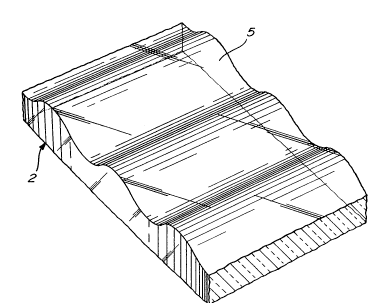
Figure 2 is an enlarged, perspective view
of the three-dimensional diffracting relief engraved
on the outer surface of the substrate of the preferred
embodiment of Figure l; and
Figure 3 is a perspective view showing the
laser beam sampling carried out by the preferred
embodiment of the holographic beam sampler.
DETAILED DESCRIPTION OF THE PREFERRED EMBODIMENT
In the different figures of the appended
drawings, the holographic beam sampler in accordance
with the present invention is generally identified by
the reference numeral 1.
The sampler 1 is simply formed of a solid,
highly transparent and substantially flat substrate 2.
Examples of materials suitable to construct the
holographic sampler are W (ultraviolet) grade fused
silica (SiO2), and zinc selenide (ZnSe). These
materials are capable of sustaining high power laser
beam. Although fused silica and zinc selenide are
given as non limitative examples, other types of
materials, having similar characteristics, can
eventually be used.
In operation, an incident high power laser
beam 3 to be sampled penetrates the substrate 2
through a planar surface 4 thereof. The laser beam 3
then propagates through the substrate 2 and leaves it
through another surface 5 thereof, opposite and
3 ~ 3.~
substantially parallel to the first surface 4, to
produce a transmitted high power laser beam 6.
A three-dimensional diffracting relief is
engraved, more specifically etched on the surface 5
directly in the fused silica or zinc selenide. As the
diffracting relief is etched directly in the material
of the substrate 2, it can also sustain the high power
laser beam 3.
An example of diffracting relief is
illustrated in Figure 2. As can be seen, this relief
is sinusoidal. More specifically, a cross section of
the substrate 2 defined by an horizontal plane in
Figures 1 and 2 will show the sinusoidal configuration
of the relief. As can be appreciated by those skilled
in the art, the diffracting relief of Figure 2 is only
an example and many other configurations of relief can
be contemplated.
As the laser beam passes through the
surface 5, the sinusoidal relief will diffract it to
extract from the transmitted high power laser beam 6,
three pairs of low power beam samples 7,8 ; 9,10 ; and
11,12. This phenomenon is well known in the art and
accordingly will not be further described in the
present specification. The different parameters and
characteristics of the transmitted laser beam 6 are
also found in the beam samples 7 - 12. In Figures 1
and 3, the beam samples 7 and 8 are first order
samples, the beam samples 9 and 10 are second order
samples, and the beam samples 11 and 12 are third
order samples.
~1 $ ,~
As can be seen in Figures 1 and 3, the
incident 3 and transmitted 6 laser beams propagate
generally in the same direction, substantially
perpendicular to the planar surface 4 and to the
engraved surface 5.
The angular distribution of the different
diffraction orders is given by the following
relationship:
~n = arcsin (nA/A) (1)
where n is the diffracted order, ~n is the angle with
respect to the transmitted beam 6, A is the wavelength
of the incident 3 and transmitted 6 laser beams, and
is the period of the sinusoidal relief. With the
preferred embodiment of the invention, the first order
angle ~1 (Figure 1) may vary between 5 and 12.
Equation (l) demonstrates that, for small angles en,
the second and third order angles ~2 and ~3 are nearly
two times and three times larger than the angle
respectively.
For low sampling factor, the relations
between the intensity of the different diffraction
orders may be expressed as
~n nn1 (2)
where ~n is the sampling factor of the nth order of
diffraction. Regarding the value of ~1~ it may be
adjusted by means of simple modifications to the
recorded relief. In practice, 10% S ~1 S 0.05%.
For example, if the ratio of the power of
each beam sample 7 and 8 to the power of the
transmitted laser beam 6 has a value Y, the ratio of
the power of each beam sample 9 and 10 to the power of
the beam 6 will be approximately y2~ and the ratio of
the power of each beam sample 11 and 12 to the power
of the transmitted beam 6 will be approximately Y3.
This is illustrated in Figure 3 by the dimensions of
the spots 13 - 19 produced by the beam 6 and beam
samples 7 - 12 on a background surface remote from but
parallel to the substrate 2 of the sampler 1 according
to the invention.
As mentioned in the foregoing description,
the diffracting relief is etched on the surface 5
directly into the material of the substrate. For
example, when high-quality fused silica is used, the
fabrication process starts with application of a
photoresistive resinous coating to the surface 5 of
the fused silica substrate 2. The coating is then
developed to record the desired relief thereon. After
development, the relief is transferred to the fused
silica surface 5 by projecting electrons on the
photoresistive coating. Although this type of etching
process is suitable to produce efficiently the thin
holographic relief required, other types of etching
processes can also be envisaged.
The holographic sampler in accordance with
the present invention offers, among others, the
following advantages:
2 ~ 3 `~
- ease in obtaining a low sampling factor
that can vary between 1/10 and 1/2000 on first order
(ratio of the power of the beam samples 7 and 8 to the
power of the transmitted beam 6);
- weak unusable losses;
- ability to preserve in the beam samples
information on the spatial profile of the transmitted
laser beam 6;
- a high damage threshold (ability to
sustain high average power, high peak power density
and high-energy pulses; at 1.064 ~m, the sampler has
shown a damage threshold as high as 86.3 J/cm2 with 10
nsec pulses);
- ability to preserve a cartesian beam (no
deviation of the transmitted beam when the incident
beam is perpendicular to the surface 4 of the
substrate 2);
- easy alignment as well as complete
independence from beam position and/or diameter;
- production of calibrated replicas of the
transmitted beam 6; and
- a very low sensitivity to light
polarization (with low diffraction angle, the sampling
factor is not affected by polarization), to
temperature variation, and generally to the
environmental conditions (various conditions of
~3 ~ ~ ~5}~ 3
temperature and humidity are expected in industrial
environments);
- no distortion of the transmitted beam
or of the samples when compared to the incident beam;
and
- no effect on the beam polarization.
Holographic beam samplers in accordance
with the present invention were proved to perform
properly at 1.064 ~m for average power levels up to 1
kW. The relative polarization sensitivity was lower
than 1.0% for diffraction angles lower than 10. Using
lS tabulated value of 1.28 x 10⁵/C for d~/dT, a relative
sensitivity on temperature variation [(1/~)d~/dT] as
low as 5,7 x 10⁵/~C was obtained.
Holographic beam samplers operating
satisfactorily at 2.1 ~m, 1.064 ~m, 694.3 nm, 532nm
and 308 nm were constructed using fused silica as the
substrate material. It should be pointed out here
that each sampler is calibrated for a specific
wavelength. W grade fused silica can be used with
wavelength varying from 250 nm to 2.1 ~m while zinc
selenide is compatible with the spectral region
extending from 2 ~m to 14 ~m.
To minimize loss, anti-reflection coating
can be applied to the surface 4 of the substrate 2.
It is also suggested to always apply an anti-
reflection coating on the surface 5. Application of
no anti-reflection coating gives a reflection of 4% on
~3
each surface 4 and 5, while application of an anti-
reflection coating on each surface 4 and 5 gives a
total reflectivity of less than 0.5%. For particular
applications, a more reflective coating can also be
applied to one or both of the surfaces 4 and 5.
As a non limitative example, holographic
beam samplers having the following characteristics can
be manufactured:
CHARACTERI8TIC5 8PECIFICATION8
Substrates W Grade Fused Silica
(from 250 nm to 2.1 ~m)
Zinc Selenide
(from 2 ~m to 14 ~m)
Diameter 1-2 inches (25.4-50.8 mm)
Thickness 0.125 inch (3.175 mm)
First Order Sample 102, or 1/100 of transmitted
(accuracy = +1%)
Second Order Sample 10-4, 1/10,000 of transmitted
(square of first order) beam
(accuracy = +2%)
Third Order Sample 106, or 1/1,000,000 of
(cube of first order) transmitted beam
l (accuracy = +3%)
¦Order Angles lst=10 2nd=20 3rd=30
Reflection Loss 0,5%
I
L ~i~ j
The example below demonstrates a typical
application with a laser source of the following type:
Pulsed Nd:YAG, 1.064 ~m, lkW.
1st order = 10-1% 1 W sample allows average
power and energy per pulse
measurement with standard
meters
2nd order = 10-4% 1 mW sample allows pulse
length measurement with a
photodetector
3rd order = 10-7% l ~W sample allows beam
profile analysis with CCD
camera and appropriate
software
I
Transmitted beam 998 W main beam allows to do
what the laser source was
designed or bought for
Another application of the holographic
beam sampler can be with a dual-wavelength copper
vapor laser for separating the yellow and green
elements in every sample in order to be able to
analyze both parts of the beam in real time while the
transmitted beam still remains intact.
A further application would be to use the
sampler of the invention as the main part of a power
and beam profile-control loop in an industrial C02 or
Nd:YAG laser system. This would allow to get the best
~ 3 3 ~ ~
performance for the system by iauto-adjustment in real
time.
In the foregoing description, the
preferred embodiment is described as comprising a
diffractive relief engraved on surface 5 of the
substrate 2. However, similar results can be obtained
by etching the diffracting relief on surface 4.
Moreover, the beam sampler 1 of the
invention operates not only with high power laser
beams, but also with low and intermediate power laser
beams.
Although the present invention has been
described hereinabove by way of a preferred embodiment
thereof, this embodiment can be modified at will,
within the scope of the appended claims, without
departing from the spirit and nature of the subject
invention.