Note: Descriptions are shown in the official language in which they were submitted.
-
Z ~ 7 ~
P9181
-- 1 --
BACKGROUND OF THE lN v~:r~.ION
1. Field of the Invention:
The present invention relates to a laminat-
ed semiconductor ceramic capacitor with a grain bound-
ary-insulated structure and a method for manufacturing
the same, and more particularly to a ceramic capacitor
which absorbs both low voltage noises and high frequen-
cy noises under normal operational conditions, and
works as a varistor against invading high voltage
pulses and high voltage static electricity, thereby
protecting built-in semiconductors and electronic
equipment from being damaged by abnormal voltages
caused by noises, pulses, and static electricity gener-
ated within the electronic equipment.
2. Description of the Prior Art:
In recent years, semiconductor devices such
as ICs and LSIs have been widely used in electronic
equipment for the purpose of realizing multifunctional
applications of the equipment and making the equipment
light, small, and handy. However, the use of many
semiconductor devices has caused the decrease in noise
resistance of the equipment. In order to maintain the
noise resistance of the electronic equipment, by-pass
capacitors such as a film capacitor, a laminated ceram-
ic capacitor, and a semiconductor ceramic capacitor
have been integrated into power source lines of various
kinds of ICs and LSIs. These capacitors exhibit excel-
lent performances in absorbing low voltage noises and
high frequency noises. However, these capacitors
themselves do not have a function of absorbing high
voltage pulses and high voltage static electricity, so
2 0 ~ 0
P9181
-- 2 --
that the invasion of high voltage pulses and high
voltage static electricity causes the malfunction of
the equipment, and the break-down of semiconductors
and/or capacitors.
As a new type capacitor, which has sufficient
pulse resistance and excellent pulse absorptivity as
well as good noise absorptivity and stability with
respect to temperature and frequency changes, a semi-
conductor ceramic capacitor with a grain boundary-
insulated structure in which a varistor function is
provided to an SrTiO3 type semiconductor ceramic capac-
itor (hereinafter, this type of capacitor is referred
to as a ceramic capacitor having a varistor function)
has been developed. This kind of ceramic capacitor is
disclosed in Japanese Laid-Open Patent Publication
Nos. 57-27001 and 57-35303. Usually, this ceramic
capacitor having a varistor function absorbs low volt-
age noises and high frequency noises, and when high
voltage pulses and high voltage static electricity
invade it, the capacitor works as a varistor, thereby
protecting the electronic equipment and built-in semi-
conductors from abnormal voltages caused by noises,
pulses, and static electricity generated in the elec-
tronic equipment. Thus, its applications have beenincreased in various fields.
Since electronic p~rts have been made light-
er, smaller, more handy, and higher in their perform-
ance, there has been a strong demand for miniaturizingand achieving high performance of a ceramic capacitor
having a varistor function. However, since a conven-
tional ceramic capacitor having a varistor function is
20584 1 0 P9181
-- 3 --
of a single-plate type, so that the effective electrode
area becomes small when the capacitor is miniaturized,
leading to a decrease in capacitance and inferior
reliability. As a solution to the above-mentioned
problems, it is considered that an electrode area be
enlarged by laminating sheet-shaped electrodes.
In general, a capacitor which does not have a
lamination structure is manufactured by a method com-
prising the steps of: sintering a ceramic sheet under a
reducing atmosphere to make ceramics of the green sheet
semiconductive; insulating a grain-boundary portion of
the semiconductive ceramics by oxidizing the green
sheet in air; and attaching an outer electrode to the
resulting green sheet. However, when this method is
applied to the above-mentioned laminated capacitor, the
following problems arise. When the green sheet having
an inner electrode on the surface thereof is laminated
and sintered, cracks are generated or the inner elec-
trode is oxidized so as to be insulated during the step
of oxidizing because of the difference in coefficient
of contraction between the inner electrode and the
ceramics constituting the green sheet. Accordingly, it
has been considered to be very difficult to manufacture
a lamination-type capacitor having a varistor function
(hereinafter, this type of capacitor is referred to as
a laminated ceramic capacitor having a varistor func-
tion) by sintering a material of the ceramic capacitor
having a varistor function and a material of the inner
electrode at the same time, wherein the material of the
ceramic capacitor includes the green sheets, a material
of outer electrodes, etc. but which excludes the mate-
rial of the inner electrode.
- 205 84l 0 P9181
As a method for simultaneously sintering a
material of the laminated ceramic capacitor having a
varistor function and a material of the inner elec-
trode, the following method for manufacturing a lami-
nated ceramic capacitor having a varistor function has
been developed and proposed, which employs processes
disclosed in Japanese Laid-Open Patent Publication
Nos. 54-53248 and 54-54250, comprising the steps of:
printing a pattern corresponding to the inner electrode
by using ceramic paste enriched in organic binder on
the surface of the ceramic substrate; sintering the
ceramic substrate to make the pattern of the inner
electrode porous; and impregnating the porous pattern
with electrically conductive metals under the appropri-
ate pressure, or alternatively a step of forming a
pattern of the inner electrode by a gilding or fusion
method. However, these processes involve many produc-
tion difficulties and they have not reached a practical
level.
Japanese Laid-Open Patent Publication
No. 59-215701 discloses a method comprising the steps
of: forming a green sheet made of ceramic powder calci-
nated under a non-oxidizing atmosphere; printing a pat-
tern of the inner electrode by using an electrically
conductive paste mixed with a thermal diffusion materi-
al on the surface of the green sheet, the thermal
diffusion material having the ability to form an elec-
trically insulated layer in a grain boundary; and
sintering the green sheet under the oxidizing atmos-
phere. Another method disclosed in Japanese Laid-Open
Patent Publication No. 63-219115 comprises the steps
of: forming a green sheet made of semiconductive ceram-
20584 1 0 P9181
ic powder as a main component, the main compone-nt being
mixed with an oxidizing agent and/or a dispersing agent
contA ~ ni ng a glass component for the purpose of forming
an insulated layer; alternately laminating the green
sheets with a plurality of inner electrodes; and sin-
tering the laminated sheets in air or under the oxidiz-
ing atmosphere. However, according to the above-men-
tioned two methods, sintering temperature is relatively
low in the range of 1,000 to 1,200C, so that the
ceramics are not readily sintered and crystal grains do
not come into contact with each other. The resulting
ceramic capacitor which is not a completely sintered
body entails shortcom;ngs including: a relatively small
electrical capacitance; a small value of voltage non-
linear index (the non-liner index is a representative
factor for showing characteristics for a varistor); and
instability of varistor voltage; and inferior reliabil-
ity as a capacitor. Moreover, in Japanese Laid-Open
Patent Publication No. 63-219115 involving the step of
adding a glass material to the ceramic powder as an
additive entails a problem in that a glass phase depos-
its in the crystal grain boundary, whereby the electri-
cal characteristics tend to be degraded and the reli-
ability of the capacitor becomes poor. Thus, this
method has not reached a practical level.
Then as described in Japanese Laid-Open Patent
Publication No. 2-240904, the present inventors have
improved a method for producing a capacitor by using a
composition of SrTiO3 containing an excess amount of Ti as
a semiconductor component and MnO2-SiO2 type compound as
a base material: and have made it possible to develop
a laminated ceramic capacitor with a varistor function
20584 ~ 0
_ P9181
-- 6 --
which has inner electrodes essentially made of Au, Pt,
Rh, Pd or Ni. Since Ni inner electrodes may cause the
oxidation of Ni at relatively lower temperatures,
thereby being insulated easily, a mixture of Ni and Pd,
or a SiTiO3 containing a slightly excess amount of Ti
has been proposed to use as an inner electrode materi-
al. However, even in this case, because Ni may be
oxidized at a re-oxidation temperature of 1200C or
more, it is difficult to obtain a substantial resolu-
tion to the above-discussed disadvantages.
As a patent concerning the laminated capaci-
tors having a varistor function, laminated voltage
non-linear elements made of ceramic material such as
ZnO, Fe203, or TiO2 have been provided in Japanese
Patent Publication No. 58-23921. This type of element
has a very small capacitance. Therefore, although it
exhibits excellent performance with respect to pulses
having a relatively high voltage and absorption of
static electricity, it exhibits little effect with
respect to noises with a voltage below the varistor
voltage or high frequency noises.
As described above, in the laminated ceramic
capacitor having a varistor function using Ni as inner
electrodes, Ni is oxidized at relatively low tempera-
tures. Therefore, depending on the production method,
Ni is oxidized and inner electrodes are insulated,
whereby electrical characteristics cannot be obtained.
Accordingly, it is expected that novel inner electrode
compositions which prevent Ni from being oxidized and a
method for manufacturing laminated ceramic capacitors
having a varistor function using such Ni inner elec-
- 20584 l 0 P9181
trodes are being developed.
SUMMARY OF THE lNv~N~lON
The laminated semiconductor ceramic capacitor
with a grain boundary-insulated structure of this
invention, which overcomes the above-discussed and
numerous other disadvantages and deficiencies of the
prior art, comprises a semiconductor ceramic block with
a grain boundary-insulated structure, a plurality of Ni
inner electrodes and outer electrodes, wherein the Ni
inner electrodes are obtained from paste containing a
powder prepared by solubilizing at least one compound
containing an atom selected from the group consisting
of Li, Na and K into Ni or an Ni containing compound;
the Ni inner electrodes are placed in a substantially
parallel manner within the ceramic block to reach thé
corresponding opposite edges of the ceramic block
alternatively one by one; and the outer electrodes are
electrically connected to the corresponding edges of
the inner electrodes, respectively.
In a preferred embodiment, the outer elec-
trodes of the capacitor are made of at least one metal
selected from the group consisting of Pd, Ag, Cu, Zn,
and Ni; an alloy thereof; or a mixture thereof.
In a preferred embodiment, the outer elec-
trodes are obtained by solubilizing at least one com-
pound containing an atom selected from the group con-
sisting of Li, Na, and K; or a combination of at least
one compound containing an atom selected from the group
consisting of Li, Na, and K and at least one compound
2Q584 1 ~ - -
-- P9181
-- 8 --
containing a Pd atom or a Pt atom into Ni or an Ni
containing compound.
In a preferred embodiment, the outer elec-
trodes comprise (1) lower outer electrodes which are
obtained by solubilizing at least one compound contain-
ing an atom selected from the group consisting of Li,
Na and K, or a combination of at least one compound
containing an atom selected from the group consisting
of Li, Na, and K and at least one compound containing a
Pd atom or a Pt atom into Ni or an Ni containing com-
pound, and (2) upper outer electrodes of an Ag or Ag-Pd
type.
In a preferred embodiment, the outer elec-
trodes are obtained by solubilizing at least one com-
pound containing a Pd atom or a Pt atom into Ni or an
Ni containing compound.
In a preferred embodiment, the outer elec-
trodes comprise (1) lower outer electrodes which are
obt~n~ by solubilizing at least one compound contain-
ing a Pd atom or a Pt atom into Ni or an Ni containing
compound, and (2) upper outer electrodes of an Ag or
Ag-Pd type.
In a preferred embodiment, the grain boundary
insulated semiconductor ceramic comprises as its main
component SrTiO3 containing an excess amount of Ti so
as to make a molar ratio of Sr to Ti in the range of
O.g5 ~ Sr/Ti < 1.00; at least one compound selected
from the group consisting of Nb205, Ta205, V205, W205,
Dy23~ Nd23~ Y203~ La203 and CeO2 in the range of
20584 1 0
- P9181
_ g _
0.05 to 2.0 mol%; and a combination of at least one
compound containing an Mn atom and at least one con-
pound containing an Si atom, the total amount of said
combination being in the range of 0.2 to 5.0 mol~ in
terms of MnO2 and SiO2, respectively.
In a preferred embodiment, the grain boundary
insulated semiconductor ceramic further comprises at
least one compound selected from the group consisting
of Na2SiO3 and Li2SiO3 in the range of
0.05 to 2.0 mol%; at least one compound selected from
the group consisting of Na2SiO3 and Li2SiO3 in the
range of 0.05 to 2.0 mol%, and A1203 in the range of
0.05 to 2.0 mol%, or at least one compound selected
from the group consisting of NaAlO2 and LiAlO2 in the
range of 0.05 to 4.0 mol%.
In place of the above-mentioned SrTiO3,
Sr(l-x)BaxTio3 or Sr(1_x)CaxTiO3 can be used.
A first method for manufacturing a l~in~ted
semiconductor ceramic capacitor with a grain boundary-
insulated structure comprises the steps of:
calcinating a mixed powder of a ceramic
composition for the formation of a grain boundary-
insulated structure in air or in a nitrogen atmosphere;
forming green sheets by dispersing the calci-
nated powder in a solvent with an organic binder and
molding the dispersed powder, the calcinaced powder
being ground before dispersing and after calcinating;
29584 1 0
-- P9181
-- 10 --
preparing a mixed powder containing at least
one compound containing an atom selected from the group
consisting of Li, Na, and K; and Ni or an Ni containing
compound;
calcinating the mixed powder in air or in a
nitrogen atmosphere to solubilize the compound contain-
ing an atom selected from the group consisting of Li,
Na, or K into the Ni or an Ni containing compound;0
grinding the calcinated mixed powder and
mixing in a solvent with an organic binder, resulting
in an inner electrode paste;
forming an inner electrode pattern by the
application of the inner electrode paste on one surface
of each of the green sheets except for the uppermost
and lowermost sheets, terminals of the inner electrodes
being extended to reach the corresponding opposite0 edges of the green sheets alternatively one by one;
laminating and compressing the green sheets
with the inner electrode pattern with the uppermost and
lowermost green sheets, followed by calcinating the
resulting green sheets in air;
sintering the calcinated sheets in a reducing
atmosphere, resulting in a sintered ceramic body with
inner electrodes;0
re-oxidizing the sintered ceramic body in
air;
29584 1 0 P9181
covering the edges of the sintered ceramic
sheets with an outer electrode paste, terminals of the
inner electrodes being exposed to the edges; and
baking the paste to form outer electrodes so
that the inner electrodes are electrically connected to
the outer electrodes.
A second method for manufacturing a laminated
semiconductor ceramic capacitor with a grain boundary-
insulated structure comprises the steps of:
l aminating and compressing the green sheets
with the inner electrode pattern of the first method
with the uppermost and lowermost green sheets of the
first method, followed by calcinating the resulting
green sheets in air;
raising the temperature of the calcinated
sheets to a temperature in the range from 1,000 to
1,200C in a nitrogen atmosphere and sintering the
calcinated sheets in a reducing atmosphere, resulting
in a sintered ceramic body with inner electrodes;
re-oxidizing the sintered ceramic body in
air;
covering the edges of the sintered ceramic
body with an outer electrode paste, terminals of the
inner electrodes being exposed to the edges, and
baking the paste to form outer electrodes so
that the inner electrodes are electrically connected to
20584 1 0
P9181
- 12 -
the outer electrodes.
A third method for manufacturing a laminated
semiconductor ceramic capacitor with a grain boundary-
insulated structure comprises the steps of:
laminating and compressing the green sheets
with the inner electrode pattern of the first method
with the uppermost and lowermost green sheets of the
first method;
covering the edges of the green sheets with
an outer electrode paste, terminals of the inner elec-
trodes being exposed to the edges, followed by calci-
nating the resulting green sheets in air;
sintering the calcinated sheets in a reducingatmosphere, resulting in a sintered ceramic body with
inner and outer electrodes;
re-oxidizing the sintered ceramic body in
air; and
re-reducing the outer electrodes.
A fourth method for manufacturing a laminated
semiconductor ceramic capacitor with a grain boundary-
insulated structure comprises the steps of:
laminating and compressing the green sheets
with the inner electrode pattern of the first method
with the uppermost and lowermost green sheets of the
first method and covering the edges of the green sheets
29584 1 0
P9181
- 13 -
with an outer electrode paste, terminals of the inner
electrodes being exposed to the edges, followed by
calcinating the resulting green sheets in air;
raising the temperature of the calcinated
sheets to a temperature in the range from 1,000 to
1,200C in a nitrogen atmosphere and sintering the
calcinated laminated sheets in a reducing atmosphere,
resulting in a sintered ceramic body with inner and
outer electrodes;
re-oxidizing the sintered ceramic body in
air; and
re-reducing the outer electrodes.
A fifth method for manufacturing a laminated
semiconductor ceramic capacitor with a grain boundary-
insulated structure comprises the steps of:0
laminating and compressing the green sheets
with the inner electrode pattern of the first method
with the uppermost and lowermost green sheets of the
first method, followed by calcinating the resulting5 green sheets in air;
covering the edges of the calcinated ceramic
sheets with an outer electrode paste, terminals of the
inner electrodes being exposed to the edges, and sin-
tering the calcinated ceramic sheets in a reducingatmosphere, resulting in a sintered ceramic body with
inner and outer electrodes;
- 2058410 P9181
- 14 -
re-oxidizing the sintered ceramic body in
air; and
re-reducing the outer electrodes.
s
A sixth method for manufacturing a laminated
semiconductor ceramic cAp~c1tor with a grain boundary-
insulated structure comprises the steps of:
laminating and compressing the green sheets
with the inner electrode pattern of the first method
with the uppermost and lowermost green sheets of the
first method, followed by calcinating the resulting
green sheets in air;
covering the edges of the calcinated ceramic
sheets with an outer electrode paste, terminals of the
inner electrodes being exposed to the edges;
raising the temperature of the calcinated
sheets to a temperature in the range from 1,000 to
1,200C in a nitrogen atmosphere and sintering the
calcinated sheets in a reducing atmosphere, resulting
in a sintered ceramic body with inner and outer elec-
trodes;
re-oxidizing the sintered ceramic body in
air; and
re-reducing the outer electrodes.
A seventh method for manufacturing a laminat-
ed semiconductor ceramic capacitor with a grain bound-
~s~
- 20584 1 0 P9181
- 15 -
ary-insulated structure comprises the steps of:
laminating and compressing the green sheets
with the inner electrode pattern of the first method
with the uppermost and lowermost green sheets of the
first method and covering the edges of the green sheets
with a lower layer outer electrode paste, terminals of
the inner electrodes being exposed to the edges, fol-
lowed by calcinating the green sheets;
sintering the calcinated sheets in a reducing
atmosphere, resulting in a sintered ceramic body with
inner electrodes and lower layer outer electrodes;
applying an upper layer outer electrode paste
containing Ag or a mixture of Ag and Pd on the lower
layer outer electrodes; and
baking the upper layer electrode paste in air
or in a nitrogen atmosphere to form upper layer outer
electrodes on the lower layer outer electrodes.
A eighth method for manufacturing a laminated
semiconductor ceramic capacitor with a grain boundary-
insulated structure comprises the steps of:
laminating and compressing the green sheets
with the inner electrode pattern of the first method
with the uppermost and lowermost green sheets of the
first method and covering the edges of the green sheets
with a lower layer outer electrode paste, terminals of
the inner electrodes being exposed to the edges, fol-
lowed by calcinating the green sheets;
29584 1 0
- P9181
- 16 -
raising the temperature of the calcinated
laminated sheets to a temperature in the range from
1,000 to 1,200C in a nitrogen atmosphere and sintering
the calcinated sheets in a reducing atmosphere, result-
ing in a sintered ceramic body with inner electrodes
and lower layer outer electrodes;
applying an upper layer outer electrode paste
containing Ag or a mixture of Ag and Pd on the lower
layer outer electrodes; and
baking the upper layer electrode paste in air
or in a nitrogen atmosphere to form upper layer outer
electrodes on the lower layer outer electrodes in air
or in a nitrogen atmosphere.
A ninth method for manufacturing a laminated
semiconductor ceramic capacitor with a grain boundary-
insulated structure comprises the steps of:
laminating and compressing the green sheets
with the inner electrode pattern of the first method
with the uppermost and lowermost green sheets of the
first method and covering the edges of the green sheets
with a lower layer outer electrode paste containing Ni,
terminals of the inner electrodes being exposed to the
edges, followed by calcinating the green sheets;
sintering the calcinated green sheets in a
reducing atmosphere, resulting in a sintered ceramic
body with inner electrodes and lower layer outer elec-
trodes;
20584 1 0
- P9181
- 17 -
re-oxidizing the sintered ceramic body in
air;
re-reducing the lower layer outer electrodes;
applying an upper layer outer electrode paste
containing Ag or a mixture of Ag and Pd on the lower
layer outer electrodes; and
baking the upper layer electrode paste to
form upper layer outer electrodes on the lower layer
outer electrodes in air or in a nitrogen atmosphere.
A tenth method for manufacturing a laminated
semiconductor ceramic capacitor with a grain boundary-
insulated structure comprises the steps of:
laminating and compressing the green sheets
with the inner electrode pattern of the first method
with the uppermost and lowermost green sheets of the
first method and covering the edges of the green sheets
with a lower layer outer electrode paste containing Ni,
terminals of the inner electrodes being exposed to the
edges, followed by calcinating the green sheets;5
raising the temperature of the calcinated
sheets to a temperature in the range from 1,000 to
1,200C in a nitrogen atmosphere and sintering the
calcinated sheets in a reducing atmosphere, resulting
in a sintered ceramic body with inner electrodes and
lower layer outer electrodes;
- 18 - P9181
re-oxidizing the sintered ceramic body in
air;
re-reducing the lower layer outer electrodes;
applying an upper layer outer electrode paste
containing Ag or a mixture of Ag and Pd on the lower
layer outer electrodes; and
baking the upper layer electrode paste to
form upper layer outer electrodes on the lower layer
outer electrodes in air or in a nitrogen atmosphere.
A eleventh method for manufacturing a lami-
nated semiconductor ceramic capacitor with a grain
boundary-insulated structure comprises the steps of:
laminating and compressing the green sheets
with the inner electrode pattern of the first method
with the uppermost and lowermost green sheets of the
first method and covering the edges of the green sheets
with a lower layer outer electrode paste, terminals of
the inner electrodes being exposed to the edges, fol-
lowed by calcinating the green sheets;5
sintering the calcinated sheets in a reducing
atmosphere;
re-oxidizing the sintered sheets in air;0
applying an upper layer outer electrode paste
containing Ag or a mixture of Ag and Pd on the lower
layer outer electrodes;
~ 20584 1 0 P9181
-- 19 --
re-reducing the sheets with inner electrodes
and lower outer electrodes on which the upper layer
outer electrode paste is applied; and
heat-treating the re-reduced sheets in air to
from upper layer outer electrodes on the lower layer
outer electrodes.
A twelfth method for manufacturing a laminat-
ed semiconductor ceramic capacitor with a grain bound-
ary-insulated structure comprises the steps of:
laminating and compressing the green sheets
with the inner electrode pattern of the first method
with the uppermost and lowermost green sheets of the
first method and covering the edges of the green sheets
with a lower layer outer electrode paste, tel ; n~l S of
the inner electrodes being exposed to the edges, fol-
lowed by calcinating the green sheets;
raising the temperature of the calcinated
laminated sheets to a temperature in the range from
1,000 to 1,200C in a nitrogen atmosphere and sintering
the calcinated sheets in a reducing atmosphere, result-
ing in a sintered ceramic body with inner electrodes
and lower layer outer electrodes;
re-oxidizing the sintered ceramic body in the
air;
applying an upper layer outer electrode paste
containing Ag or a mixture of Ag and Pd on the lower
layer outer electrodes;
2 0 5 8 4 1 0
- P9181
- 20 -
re-reducing the sintered ceramic body with
inner electrodes and lower outer electrodes on which
the upper layer outer electrode paste is applied: and
heat-treating the re-reduced ceramic body in
air to form upper layer outer electrodes on the lower
layer outer electrodes.
A thirteenth method for manufacturing a
laminated semiconductor ceramic capacitor with a grain
boundary-insulated structure comprises the steps of:
laminating and compressing the green sheets
with the inner electrode pattern of the first method
with the uppermost and lowermost green sheets of the
first method, followed by calcinating the green sheets
in air;
covering the edges of the calcinated sheets
with a lower layer outer electrode paste, terminals of
the inner electrodes being exposed to the edges, and
sintering the calcinated sheets in a reducing atmos-
phere;
applying an upper layer outer electrode paste
containing Ag or a mixture of Ag and Pd on the lower
layer outer electrodes; and
baking the upper layer outer electrode paste
to form upper layer outer electrodes on the lower layer
outer electrodes in air or in a nitrogen atmosphere.
29584 1 0
- P9181
- 21 -
A fourteenth method for manufacturing a lami-
nated semiconductor ceramic capacitor with a grain
boundary-insulated structure comprises the steps of:
laminating and compressing the green sheets
with the inner electrode pattern of the first method
with the uppermost and lowermost green sheets of the
first method, followed by calcinating the resulting
green sheets in air;
covering the edges of the green sheets with a
lower layer outer electrode paste, terminals of the
inner electrodes being exposed to the edges, and rais-
ing the temperature of the calcinated laminated sheets
to a temperature in the range from 1,000 to 1,200C in
a nitrogen atmosphere, followed by sintering the calci-
nated laminated sheets in a reducing atmosphere, re-
sulting in a sintered ceramic body with inner elec-
trodes and lower layer outer electrodes;
applying an upper layer outer electrode paste
containing Ag or a mixture of Ag and Pd on the lower
layer outer electrodes; and
baking the upper layer outer electrode paste
to form upper layer outer electrodes on the lower layer
electrodes in air or in a nitrogen atmosphere.
A fifteenth method for manufacturing a lami-
nated semiconductor ceramic capacitor with a grain
boundary-insulated structure comprises the steps of:
20584 ~ 0
- P9181
- 22 -
laminating and compressing the green sheets
with the inner electrode pattern of the first method
with the uppermost and lowermost green sheets of the
first method, followed by calcinating the resulting
green sheets in air;
covering the edges of the green sheets with a
lower layer outer electrode paste, terminals of the
inner electrodes being exposed to the edges, followed
by sintering the green sheets in a reducing atmosphere
to obtain a sintered ceramic body with inner electrodes
and lower layer outer electrodes;
re-oxidizing the sintered ceramic body in
air;
re-reducing the re-oxidized sintered ceramic
body;
applying an upper layer outer electrode paste
containing Ag or a mixture of Ag and Pd on the lower
layer outer electrodes; and
baking the upper layer outer electrode paste
to form upper layer outer electrodes on the lower layer
outer electrodes in air or in a nitrogen atmosphere.
A sixteenth method for manufacturing a lami-
nated semiconductor ceramic capacitor with a grain
boundary-insulated structure comprises the steps of:
laminating and compressing the green sheets
with the inner electrode pattern of the first method
- 23 - P9181
with the uppermost and lowermost green sheets of the
first method, followed by calcinating the resulting
green sheets in air;
covering the edges of the calcinated sheets
with a lower layer outer electrode paste, terminals of
the inner electrodes being exposed to the edges, fol-
lowed by raising the temperature of the calcinated
sheets to a temperature in the range from 1,000 to
l,200C, followed by sintering in a reducing atmosphere
to obtain a sintered ceramic body with inner electrodes
and lower layer outer electrodes;
re-oxidizing the sintered ceramic body in
air;
re-reducing the sintered and re-oxidized
ceramic body;
applying an upper layer outer electrode paste
containing Ag or a mixture of Ag and Pd on the lower
layer outer electrodes; and
baking the upper layer outer electrode paste
to form upper layer outer electrodes on the lower layer
outer electrodes in air or in a nitrogen atmosphere.
A seventeenth method for manufacturing a
laminated semiconductor ceramic capacitor with a grain
boundary-insulated structure comprises the steps of:
laminating and compressing the green sheets
with the inner electrode pattern of the first method
20584 1 0 P9181
- 24 -
with the uppermost and lowermost green sheets of the
first method, followed by calcinating the resulting
green sheets in air:
covering the edges of the green sheets with a
lower layer outer electrode paste, terminals of the
inner electrodes being exposed to the edges, followed
by sintering the green sheets in a reducing atmosphere
to obtain a sintered ceramic body with inner electrodes
and lower layer outer electrodes;
re-oxidizing the sintered ceramic body in
air;
applying an upper layer outer electrode paste
containing Ag or a mixture of Ag and Pd on the lower
layer outer electrodes;
re-reducing the sintered and re-oxidized
ceramic body; and
heat-treating the sintered re-oxidized, and
re-reduced ceramic body in air.
An eighteenth method for manufacturing a
laminated semiconductor ceramic capacitor with a grain
boundary-insulated structure comprises the steps of:
laminating and compressing the green sheets
with the inner electrode pattern of the first method
with the uppermost and lowermost green sheets of the
first method, followed by calcinating the resulting
green sheets in air;
20584 1 0 P9181
- 25 -
covering the edges of the green sheets with a
lower layer outer electrode paste, terminals of the
inner electrodes being exposed to the edges, and rais-
ing the temperature of the green sheets to a tempera-
ture in the range from 1,000 to 1,200C in a nitrogen
atomosphere, followed by sintering in a reducing atmos-
phere to obtain a sintered ceramic body with inner
electrodes and lower layer outer electrodes;
re-oxidizing the sintered ceramic body in the
air;
applying an upper layer outer electrode paste
containing Ag or a mixture of Ag and Pd on the lower
layer outer electrodes;
.
re-reducing the sintered and re-oxidized
ceramic body; and
heat-treating the sintered, re-oxidized, and
re-reduced ceramic body in air.
A nineteenth method for manufacturing a
laminated semiconductor ceramic capacitor with a grain
boundary-insulated structure comprises the steps of:
laminating and compressing the green sheets
with the inner electrode pattern of the first method
with the uppermost and lowermost green sheets of the
first method, followed by calcinating the resulting
green sheets in air;
20584 1 0
P9181
- 26 -
sintering the green sheets in a reducing
atmosphere, resulting in a sintered ceramic body;
re-oxidizing the sintered ceramic body in
air;
covering the edges of the sintered ceramic
body with a lower layer outer electrode paste, termi-
nals of the inner electrodes being exposed to the
edges, and baking the lower layer outer electrode paste
in a reducing or in a nitrogen atmosphere;
applying an upper layer outer electrode paste
containing Ag or a mixture of Ag and Pd on the lower
layer outer electrodes; and
baking the upper layer electrode paste to
form upper layer outer electrodes on the lower layer
outer electrodes in air or in a nitrogen atmosphere.
A twentieth method for manufacturing a lami-
nated semiconductor ceramic capacitor with a grain
boundary-insulated structure comprises the steps of:
laminating and compressing the green sheets
with the inner electrode pattern of the first method
with the uppermost and lowermost green sheets of the
first method, followed by calcinating the resulting
green sheets in air;
raising the temperature of the green sheets
to a temperature in the range from 1,000 to 1,200C and
sintering the green sheets in a reducing atmosphere,
20584 l O P9181
- 27 -
resulting in a sintered ceramic body;
oxidizing the sintered ceramic body in air;
covering the edges of the sintered ceramic
body with a lower layer outer electrode paste, termi-
nals of the inner electrodes being exposed to the
edges, and baking the lower layer outer electrode paste
in a reducing or in a nitrogen atmosphere;
applying an upper layer outer electrode paste
containing Ag or a mixture of Ag and Pd on the lower
layer outer electrodes; and
baking the upper layer outer electrode paste
to form upper layer outer electrodes on the lower layer
outer electrodes in air or in a nitrogen atmosphere.
Thus, the invention described herein makes
possible the objectives of: (1) providing a laminated
semiconductor ceramic capacitor with a grain boundary-
insulated structure having a varistor function which
absorbs low voltage noises and high frequency noises
under the normal operational conditions and works as a
varistor when high voltage pulses and high voltage
static electricity invade the circuit; (2) providing a
laminated semiconductor ceramic capacitor with a grain
boundary-insulated structure having a varistor function
which contains as its main component SrTiO3, in which
the ceramic capacitor material and the inner electrode
material are simultaneously sintered; (3) providing a
laminated semiconductor ceramic capacitor with a grain
boundary-insulated structure having a varistor function
20584 l 0 P9181
- 28 -
which includes Ni as its inner electrodes; and
(4) providing a method for manufacturing a laminated
semiconductor ceramic capacitor with a grain boundary-
insulated structure having a varistor function which
has the above-mentioned properties.
BRIEF DESCRIPTION OF THE DRAWINGS
This invention may be better understood and
its numerous objects and advantages will become appar-
ent to those skilled in the art by reference to the
accompanying drawings as follows:
Figure 1 is a flow chart showing a process
for manufacturing a laminated ceramic capacitor with a
varistor function of Example 1 of the present inven-
tion.
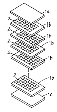
Figure 2 is an exploded perspective view
illustrating an example of the laminated ceramic capac-
itor with a varistor function according to the present
invention and showing laminated green sheets and a
pattern of the inner electrode paste printed on the
green sheets.
Figure 3 is a partially cutaway view of the
laminated ceramic capacitor with a varistor function
obtained from Examples 1 to 7 of the present invention.
Figure 4 is a flow chart showing a process
for manufacturing a laminated ceramic capacitor with a
varistor function in Example 2 of the present inven-
tion.
20584 1 0
P9181
- 29 -
Figure 5 is a flow chart showing a process
for manufacturing the laminated ceramic capacitor with
a varistor function in Examples 3 and 4 of the present
invention.
Figure 6 is a flow chart showing a process
for manufacturing the laminated ceramic capacitor with
a varistor function in Example 5 of the present inven-
tion.
Figure 7 is a flow chart showing a process
for manufacturing the laminated ceramic capacitor with
a varistor function in Example 6 of the present inven-
tion.
Figure 8 is a flow chart showing a process
for manufacturing the laminated ceramic capacitor with
a varistor function in Example 7 of the present inven-
tion.
Figure 9 is a partially cut away view showing
the laminated ceramic capacitor with a varistor func-
tion obtained from Examples 8 to 21 of the present
invention.
Figure 10 is a flow chart showing a process
for manufacturing the laminated ceramic capacitor with
a varistor function in Example 8 of the present inven-
tion.
Figure 11 is a flow chart showing a process
for manufacturing the laminated ceramic capacitor with
a varistor function in Example 9 of the present inven-
20584 ~ 0
- P9181
- 30 -
tion.
Figure 12 is a flow chart showing a process
for manufacturing the laminated ceramic capacitor with
a varistor function in Example 10 of the present inven-
tion.
Figure 13 is a flow chart showing a process
for manufacturing the laminated ceramic capacitor with
a varistor function in Example 11 of the present inven-
tion.
Figure 14 is a flow chart showing a process
for manufacturing the laminated ceramic capacitor with
a varistor function in Example 12 of the present inven-
tion.
Figure 15 is a flow chart showing a process
for manufacturing the laminated ceramic capacitor with
a varistor function in Example 13 of the present inven-
tion.
Figure 16 is a flow chart showing a process
for manufacturing the laminated ceramic capacitor with
a varistor function in Example 14 of the present inven-
tion.
Figure 17 is a flow chart showing a process
for manufacturing the laminated ceramic capacitor with
a varistor function in Example 15 of the present inven-
tion.
- 20584 ~ 0
P9181
- 31 -
Figure 18 is a flow chart showing a process
for manufacturing the laminated ceramic capacitor with
a varistor function in Example 16 of the present inven-
tion.
Figure 19 is a flow chart showing a process
for manufacturing the laminated ceramic capacitor with
a varistor function in Example 17 of the present inven-
tion.
Figure 20 is a flow chart showing a process
for manufacturing the laminated ceramic capacitor with
a varistor function in Example 18 of the present inven-
tion.
Figure 21 is a flow chart showing a process
for manufacturing the laminated ceramic capacitor with
a varistor function in Example 19 of the present inven-
tion.
Figure 22 is a flow chart showing a process
for manufacturing the laminated ceramic capacitor with
a varistor function in Example 20 of the present inven-
tion.
Figure 23 is a flow chart showing a process
for manufacturing the laminated ceramic capacitor with
a varistor function in Example 21 of the present inven-
tion.
20584 1 0
P9181
- 32 -
DESCRIPTION OF THE PREFERRED EMBODIMENTS
When a ceramic capacitor with a varistor
function is manufactured, a ceramic element which is
5made semiconductive under a reducing or a nitrogen
atmosphere should be sub;ected to a heat treatment in
air (hereinafter this heat treatment is referred to as
re-oxidation) to provide its crystal grain boundaries
with high resistance. Therefore, the following two
10subjects are the most important in the case of manufac-
turing a laminated ceramic capacitor with a varistor
function: First, inner electrodes are excellent in
oxidation resistance; and secondly, the crystal bound-
aries of the ceramic element are excellent in oxidation
15properties. It means that the inner electrodes and
the ceramic element require opposite characteristics in
the re-oxidation process.
Therefore, when a laminated ceramic capacitor
20with a varistor function having Ni inner electrodes
according to the present invention is manufactured, the
following subject arises: The oxidation resistance of
the Ni inner electrodes should be improved, and simul-
taneously the oxidation properties of the crystal
25boundaries of a ceramic element should also be im-
proved. The present inventors have found that (1) the
oxidation resistance of the Ni inner electrodes is
improved by solubilizing at least one compound contain-
ing an atom selected from the group consisting of Li,
30Na and K into Ni or an Ni-containing compound which
produces a P-type oxide to reduce the oxidation rate;
and (2) at least one atom selected from the group
consisting of Li, Na, and K which is added to the Ni
20584 1 0
- P9181
- 33 -
inner electrodes is readily dispersed in the crystal
boundaries of a ceramic element during the re-oxidation
step, and works as an oxygen carrier, thereby acceler-
ating the oxidation of the crystal boundaries.
According to the present invention, it is
possible to improve both the oxidation resistance of
the Ni inner electrodes, and the oxidation properties
of the crystal boundaries of a ceramic element by
solubilizing at least one compound containing an atom
selected from the group consisting of Li, Na and K into
Ni or an Ni-cont~ning compound, which makes it possi-
ble to readily manufacture a laminated ceramic capaci-
tor with a varistor function having Ni inner elec-
trodes.
Examples
The present invention will be described byway of illustrating the following examples.
Example l
First, a Li2CO3 powder in the range of
0.05 to 2.5 mol~ was added to a NiO powder having an
average particle size of 0.5 ,um or less and a purity of
90~, and the mixture was calcinated in air at a temper-
ature in the range of 500 to 1,300C. The calcinated
powder was ground again so as to make an average parti-
cle size of 1.5 ,um or less and provided as a starting
material for inner electrodes. The powdered starting
material was dispersed in a solvent together with an
organic binder such as a butyral resin to form an
inner electrode paste. Then, as shown in Figure 2,
97 mol% of SrTiO3 (Sr/Ti=0.97) powder, 1 mol% of Nb2O5
20584 1 0 P9181
- 34 -
powder, 1 mol% of MnO2 powder, and 1 mol% of SiO2
powder were mixed and formed into green sheets lb with
a thickness of about 50 ~m by the doctor blade method,
followed by cutting into a predetermined size. Pat-
terns of the inner electrode paste 2 were printed on
the green sheets lb obtained as shown in Figure 2 in
accordance with a predetermined size. As is apparent
from Figure 2, the inner electrode paste 2 was not
printed on the uppermost and lowermost green sheets la
and lc. Usually, a plurality of the green sheets lb
are laminated. The patterns of the inner electrode
paste 2 were printed on intermediate layers of the
laminated green sheets 1 so as to reach one edge of
the sheet, and the green sheets lb are stacked in such
a manner that the edges which the inner electrodes
reach are alternately overlaid and the edges which the
inner electrodes do not reach are alternately overlaid.
Then, the uppermost and lowermost green sheets la and
lc were placed on the uppermost and lowermost parts,
respectively, and the green sheets lb printed with the
above inner electrode paste 2 thereon were laminated
therebetween. The resulting laminated green sheets lb
were heat-pressed and contacted together with the
uppermost and lowermost green sheets la and lc to
obtain a laminated body 1. The laminated body 1 was
heated at a temperature in the range of 600 to 1,250C
in air so as to remove the above binder therefrom,
whereby the laminated body was calcinated. The calci-
nated body was next sintered by heating to a tempera-
ture in the range of 1,200 to 1,350C in a reducing
atmosphere, followed by re-oxidation by heating at a
temperature of 900 to 1,100C in air. As shown in
Figure 3, the outer electrode paste containing Ag was
20584 ~ 0
- P9181
- 35 -
coated on both edges of the semiconductor ceramic with
a grain boundary-insulated structure (hereinafter, this
semiconductor ceramic is referred to as a ceramic
element) in which terminals of the inner electrodes 2a
were exposed alternatively in the opposite directions,
and the Ag paste was baked by heating at 800C for
15 minutes in air, thereby obt~i~;ng a laminated ceram-
ic capacitor 4 with a varistor function, comprising a
plurality of inner electrodes 2a in the ceramic ele-
ment, the terminals of the inner electrodes 2a re~h;ng
each opposite edge of the ceramic element alternatively
one by one; and outer electrodes 3 placed at opposite
edges of the ceramic element so that the outer elec-
trodes 3 can be electrically connected to the terminals
of the inner electrodes 2a.
Size of the laminated ceramic capacitor with
a varistor function, abbreviated as Type 5.5, is
5.70 mm in width, 5.00 mm in length, and 2.00 mm in
thickness. The capacitor is composed of 10 layers on
which patterns of the inner electrodes are printed.
Figure 1 is a flow chart showing a manufacturing proc-
ess according to present invention.
In the laminated ceramic capacitor with a
varistor function thus manufactured, various kinds of
electrical characteristics such as a capacitance,
tan ~, a varistor voltage, a voltage non-linear
index a, an equivalent series resistance (ESR), a
capacitance-temperature change rate, and a temperature
coefficient of varistor voltage are shown in Tables
1 to 5, varying with the re-oxidation temperatures.
20~84 ~ ~ -
P9181
- 36 -
The experimental conditions for preparing
laminated samples were 1,200C, 2 hours for removal of
the binder and calcination in air; and 1,300C, 2 hours
for sintering in a reducing atmosphere of N2:H2 = 99:1.
The inner electrode paste contains a powder prepared by
calcinating a mixed powder of NiO and Li2C03 (the
amount of LiCO3 is 0 to 2.5 mol% based on the total
moles of NiO and Li2CO3) at 1,100C for 2 hours in
air.
1 0
Each electrical characteristic was obtained
under the following experimental conditions.
* Capacitance (C) was measured at 1.0 V and 1.0 kHz.
* Varistor voltage V0 lmA was measured at 0.1 mA.
* Voltage non-linear index a was calculated from the
values of varistor voltage measured at 0.1 mA and
1.0 mA, respectively, using the following equation:
a = 1 / log (VlmA/vo~lmA)
* Equivalent series resistance (ESR) is defined as
resistance at the resonance frequency measured at
1.0 V.
* Capacitance-temperature change rate was obtained from
the following equation:
Capacitance-temperature change rate (%) =
Capacitance at 85C - (Capacitance at -25C) x 100
Capacitance at -25C
* Temperature coefficient of varistor voltage was
obtained by the following equation:
2~584 ~0 P9181
- 37 -
Temperature coefficient of varistor voltage =
Varistor voltage - Varistor voltage
at 50C at 25C x 100
(50 - 25) x Varistor voltage at 25C
20584 l 0 P9181
- 38 -
Table 1
Re-oxidation: 900 C Ag outer el~ctrode
SrTiO3(Sr/Ti=0.97)
Nb2o5 0.5 mol% MnO2: 1.0 mol% SiO2: 1.0 m~l%
Inner
ele~de C ~ ~ V ~ ESR ~C/C ~V/V
No. L12C~3 . 0.1mA
( 1%) (nF) (%~ (V) (mQ) (%) (%)
* 1 0.0~3 81 1.9 5 ~ 41 - 4.5 - 2.8
2 ~.0 ~37 4 1.9 7 1 2 3 8 - 3.4 - 2.~
3 0.1 03 67 1.8 8 1 3 3 6 - 3.1 - 1.6
4 0.2 03 ~9 1.7 8 1 5 2 7 - 2.g - 1.5
0.~ ~3 22 1.~ 9 1 6 ~7 - ~.6 - 1.1
6 ? ~ 28g 1. 6 l o 1 3 28 - 2.7 - 1.3
7 1.0 ~~ 3 1.6 1 2. 1 2 3 1 - ~.0 - 1.6
8 1.5 ~1 8Q 1.7 i~ 1 0 3 ~ - 3.1 - 1.7
9 ~ 8 1.~ 2 2 ~ 42 - 3.7 - 2.2
* 1 ~ 2.~ 0 -~2 3.1 .~ ~ ~ 5 2 - 4.~ - 3.8
20584 1 0
P9181
- 39 -
Table 2
Re-oxidation: 950C Ag outer electrode
SrTiO3(Sr/Ti=0.97)
Nb20s: 0.5 mol% MnO2 1.0 mol~ SiO2: 1.0 mol~
~le Inner
No. ~e~l~de tan~ V0.1 mA ~ ESR ~C/C V/V
(1~`01%) (nF) (V) ' tmQ ) (%) (%)'
*11 0.00 98 1.~ 32 7 250 -4.~ -2.6
1 8 3 1. 71 2 1 0 4 5 - 3. 1 - 2. 0
1 3 0 . 1 0 ~ 0 0 1 . 7 1 3 1 2 3 8 - 3 . 0 - 1 . 6
14 ~.2û 224 1.7 13 1431 -2.9
~.~iO 24~ 1.5 15 1~32 -2.6 ~
16 0.73 241 1.3 18 1334 -2. / -1.3
1 7 1. 0 0 2 3 3 1. 6 2 0 1 1 3.5 ~ ' . 7
18 1.50 160 1.7 30 1038 -3.1 -1.8
19 2.00 108 1.9 35 . 9 4t~ -3.4 -2.1
*20 2.~0 4a 4.3 44 558 -4.4 -3.8
- 20584 7 0 P9181
- 40 -
Table 3
Re-oxidation: 1~00C Ag outer electrode
SrTiO3(Sr/Ti=0.97)
Nb25: 0.5 mol~ MnO2: 1.O mol% SiO2: 1.O mol~
~le Inner
No. electrode C ~ ~ V0 1mA ~ ESR ~C/C AV/V
(m~1%~ (nF) (%) (V) (mQ) (%) (%).
*21 0.00 32 1.3 Ga 5 1000 -4.8 -2.8
2 2 û . û a 1 1 a 1. 5 1 8 9 4 8 - 3 . 2 --1 . 9
0 . 1 0 1 ~ 2 1 . 5 1 ~ 1 0 4 ~ - 3 . 0 - 1 . ~
24 0.2.~ 171 .1.~ 1~ 12 42 -2.7 -1.4
. 0.50 204 1.5 17. 12 34 -2.a -û.9
2 6 0. I a 211 1. 5 1 ~ 12 3 6 - 2.. 7 -1. 3
2 7 1. 0 0 2 0 4 1. ~ ~ 1 g 4~ - 3. 0 - 1. 5
2 8 1 . ~ 0 1 ~ 3 3 8 4 2 - 3. 0 - 1. 7
2 9 2. ~ 0 g 5 1. 7 3 8 7 S ~ - 3. 3
*30 2.50 35 2.1 43 a cl -4.2 -3.
. .
P9181
- 41 -
20~84 ~ ~
Table 4
Re-oxidatio~ 10~0C Ago~ter electrode
SrTiO3(Sr/Ti=0.97)
Nb205: 0.5 mol% MnO2, 1.O mol% SiO2: 1.O mol%
~rle Inner
No. ele~L~de
Li2CO3 C tan~ V0.1 mA ~ ESR ~C/C AV/V
(mo1%) (nF~ (V) (m~
* 31 0. 0 0 0. ~ 1. 0 4 a 7 ~ 4. ~ - ~. 8
3 2 0. 0 ~ 7 4 1. 4 2 ~ 8 ~ . 3 - 1. 8
33 0.10 112 1.5 21 9 48 -3.2 -1.7
34 C.20 127 1.5 21 10 45 -3.2 -1.~
3 5 0 . ~ 0 1 3 8 1 . ~ 2 2 1 1 3 7 - 2 . 7 - 1 . 0
3 ô ~. 7 5 1 9 1 1 . ~ 2 3 1 1 3 g ` - 2. 6 - 1 . 3
37 1.00 . 175 1.5 23 8 42 -3.0 -1.6
3 8 1 . 5 0 1 2 4 1 . 3 3 5 8 5 1 - 3 . 2 - i . 7
3~ 2.00 82 1.9 4~ 7 61 -3.4 -2.2
~40 2.50 31 2.6 ~2 5 65 -4.3 -3.4
P9181
- 42 -
29584 1 0
Table 5
Re-oxidation : l1oocc Ag out~r electrode
SrTiO3(Sr/Ti=0.97)
Nb2o~: 0.5 mol~ ~nO2: 1.0 mol% SiO2 1.0 mol~
~le Inner
No. ele Lvde C ~ ~ V0.1mA ~ E5R AC/C ~V/V
%) (nF) (%) (V) (mQ
*41 0. 00 ~ 0. 8 OVER 2 6287 ~4. 8 -2.7
4 2 O 5 3 3 1 . 4 3 6 8 3 ~i ~ 3 . 4 ~ 1 . 8
4 3 0 . i O 7 1 1 . 4 2 7 9 ~ 2 ~ 3 . 3 ~ 1 . 7
44 0. ~ 0 7 8 1. 4 2 7 9 ~ 1 ~ 2. 7 ~ 1. ~
0.50 100 1.4 27 9 42 -2.2 -1.2
46 ~). 7 5 ~ 7 2 1. 4 2 9 9 ~ 1 ~ 2. 4 ~ 1. 3
4 7 1 . O ~) 1 5 4 1 . 4 3 1 8 - 3 '~ - 3 . t) - 1 .
48 1. 5 O 1 O ~ 1. 5 3 3 7 5 9 ~ 3. 1 ~ 1. ~
4 9 2. O O 7 2 1. ~ ~ 1 6 6 g ~ 3. ;) -2. 8
5 ~) ~ . 5 0 2 4 2 . 3 6 1 4 8 }. ~ 4. 9 ~ 3 . 7
~~ P9181
- 43 - ?~ 10
The samples marked by the symbol * in Tables
l to 5 are comparative examples. The Ni inner elec-
trodes of these sintered elements marked by the
symbol * are significantly oxidized. The capacitor
5having these inner electrodes cannot exhibit the per-
formances as both of a normal capacitor which absorbs
low voltage noises and high frequency noises, and of a
varistor which absorbs high voltage pulses and high
voltage static electricity, at the same time. More-
10over, this kind of capacitor has a large capacitance-
temperature change rate and a large temperature coeffi-
cient of varistor voltage due to the presence of an
unreacted Li ion, whereby reliability and electrical
characteristics of the capacitor are liable to be
15influenced by temperature change. Therefore, these
samples are not suitable as a ceramic capacitor with a
varistor function which protects semiconductors and
electronic equipment from abnormal voltages such as
noises, pulses, and static electricity generated in the
20electronic equipment. On the other hand, the other
samples which are not marked by the symbol * possess a
large capacitance, a large value of voltage non-linear
index a and a small equivalent series resistance (ESR).
A capacitor with these characteristics exhibits the
25performances both of a normal capacitor which absorbs
low voltage noises and high frequency noises, and of a
varistor which absorbs high voltage pulses and high
voltage static electricity. Moreover, this kind of
capacitor has a small capacitance-temperature change
30rate and a small temperature coefficient of varistor
voltage, whereby reliability and electrical character-
istics are not liable to be influenced by temperature
change. Therefore, these samples are well suited for
20584 7 0
--- P9181
- 44 -
use as a ceramic capacitor with a varistor function
which protects semiconductors and electronic equipment
from abnormal voltages such as noises, pulses, and
static electricity generated in the electronic equip-
ment.
The amount of Li2CO3 contained in the inner
electrode paste in this example was adjusted in the
range of 0.05 to 2.0 mol~ based on the total moles of
NiO and Li2C03 for the following reasons. When the
amount of Li2CO3 is less than 0.05 mol~, the effect of
the added material is hardly obtained and the Ni inner
electrodes are significantly oxidized as the re-oxida-
tion temperature rises. On the other hand, when the
amount of Li2C03 is more than 2.0 mol%, the presence of
a great amount of unreacted Li ions may influence the
elect-rical characteristics and reliability of the
resulting laminated ceramic capacitor. Therefore, it
can be seen that when the added amount of Li2C03 is in
range of 0.05 to 2.0 mol~, (1) the oxidation resistance
of the Ni inner electrodes is improved, (2) Li atoms
are readily dispersed in the crystal boundaries of the
ceramic element and work as oxygen carriers, thereby
accelerating the oxidation of the crystal boundaries,
which results in the improvement of the varistor func-
tion of the laminated ceramic capacitor, and (3) the
capacitance-temperature change rate and temperature
coefficient of varistor voltage of the resulting lami-
nated semiconductor capacitor are also improved. For
these reasons, the variation of the amount of Li2C03
added to the inner electrode paste is expected to
provide a laminated ceramic capacitor with a varistor
function which has different electrical characteristics
20584 1 0 P9181
- 45 -
and excellent temperature characteristics.
Although a mixture of NiO and Li2CO3 was used
as a powdered starting material as an inner electrode
paste in this example, NiO may be replaced by Ni, or
Ni-containing carbonates, hydroxides, nitrates, or the
like; Li2CO3 may be replaced by Li-containing oxides,
hydroxides, fluorides, silicates, aluminates, or the
like, and Li may be replaced by Na-containing or
K-containing oxides, hydroxides, fluorides, silicates,
aluminates, or the like, which provides the same effect
as achieved herein.
Also, a mixture of two or more kinds of Li,
Na and K may be used in this material.
Although Ag was used as an outer electrode
material in this example, it was confirmed that other
materials such as Pd, Cu, Zn, and Ni may provide the
same effect. This means that at least one metal select-
ed from the group consisting of Pd, Ag, Cu, Zn, and Ni,
an alloy thereof, or a mixture thereof may be used as
an outer electrode material. Moreover, it was confirmed
that Ni outer electrodes which are made of an outér
electrode paste prepared by solubilizing at least one
compound containing an atom selected from the group
consisting of Li, Na, and K into Ni or an Ni-containing
compound may provide the same effect.
It was also confirmed that Ni outer elec-
trodes made of an outer electrode paste prepared by
solubilizing a combination of at least one compound
containing an atom selected from the group consisting
20584 l 0 P9181
- 46 -
of Li, Na, and K and at least one compound containing a
Pd atom or a Pt atom into Ni or an Ni-containing com-
pound may provide the same effect.
However, when an atom such as Cu, Zn, and Ni
is present in the outer electrodes, it is required to
lower the baking temperature, to shorten baking time,
and to control the atmosphere in which the baking is
carried out because these atoms tend to be oxidized.
The effect in withstanding surge current
(maximum current wave value observed under the condi-
tion that the variation of a varistor voltage VO lmA is
within + 10~ when 8 x 20 ~s of impulse current is
applied twice at 5-minute interval in the same direc-
tion) of the samples obtained in this example was
measured to be in the range of 300 to 400 A, which
indicated the same characteristics as, or better char-
acteristics than the conventional ZnO type varistors.
Also, it was found that the laminated ceramic
capacitor having the inner electrodes of the present
invention had excellent effect in withstanding surge
current for the following reasons, compared to those
having the inner electrodes with the same structure
made of Au, Pt, Rh, Pd, and the like. At least one
atom selected from the group consisting of Li, Na, and
K which is added to inner electrodes forms (1) a firm
insulated layer in the grain boundaries of a ceramic
element, and works as a sintering assistant to provide
(2) a tight adhesiveness between the inner electrodes
and the ceramic element. Thus, the laminated ceramic
capacitor is not likely to be destroyed because of the
2g584 lO P9181
- 47 -
above firm insulated layer and flashover is hardly
generated because of the tight adhesiveness between the
inner electrodes and the ceramic element.
The laminated ceramic capacitor with a varis-
tor function thus manufactured has larger capacitance
and exhibits much better temperature and frequency
characteristics than the laminated varistor disclosed
in the above-mentioned Japanese Patent Publication
No. 58-23921. The laminated ceramic capacitor in the
present invention is manufactured by laminating ceramic
capacitor materials with a varistor function which can
form a capacitor which possesses both functions of a
normal capacitor which absorbs noises, and of a varis-
tor which absorbs pulses and static electricity, while
the above-mentioned varistor in the prior art is simply
made of piled varistor materials which show prominent
absorbing ability for surge current. The laminated
ceramic capacitor with a varistor function in the
present invention is completely different from the
varistor in the prior art in both functions and uses.
Example 2
A laminated body prepared by using green
sheets and an inner electrode paste having the same
composition as that in Example 1 was heated at a tem-
perature in the range of 600 to 1,250C in air to
remove the binder, whereby the laminated body was
calcinated. The calcinated body was sintered by heat-
ing to a temperature in the range of 1,000 to 1,200C
in a nitrogen atmosphere and then at a temperature in
the range of 1,200 to 1,350C in a reducing atmosphere,
followed by re-oxidation by heating at a temperature of
20584 7 0
- P9181
- 48 -
900 to 1100C in air. Then, the outer electrode paste
containing Ag was coated on both edges of the ceramic
element in which terminals of the inner electrodes were
exposed alternatively in the opposite directions, and
the Ag paste was baked by heating at 800C for
15 minutes in air, thereby obtaining a laminated ceram-
ic capacitor with a varistor function. The various
electrical characteristics of the resulting laminated
ceramic capacitor with a varistor function are shown in
Tables 6 to 10.
The experimental conditions for preparing
laminated samples were 1,200C, 2 hours for calcination
in air; a total of 2 hours for heating at 1,200C in a
nitrogen atmosphere and at 1,300C in the reducing
atmosphere of N2 : H2 = 99 : 1; and 900-1,100C,
2 hours for re-oxidation in air. Also, the inner elec-
trode paste and the outer electrode paste were prepared
by calcinating a mixed powder of NiO and Li2C03 at
1,100C for 2 hours in air. Figure 4 is a flow chart
showing the manufacturing process.
The other manufacturing conditions such as
the number of laminated sheets were identical to those
in Example 1, and various electrical characteristics
were measured as described therein.
20584 ~ 0 P9181
- 49 -
Table 6
Re-oxidation: 900C - Ag outer electrode
SrTiO3(Sr/Ti=0.97)
Nb2O~: 0.5 mol~ MnO2: 1.Omol% SiO3: 1.0 mol%
Eample Inner
~o. ele~ de C tan ~ V0 1mA a ESR ~ c/c ~v/v
Li2o~,
(mol%~ (nF) (%) (V) (m~ J
51 0.00 3 ~8 1.9 ~ 8 40 - 4.~ - 2.8
5 2 5.0 5 ~8~ 1.9 7 1 2 37 - 3.4 ~ ~.0
53 ~.1 037 5 ~.8 8 13 3 5 - 3.1 - 1.6
~4 0.2 036 8 1.7 8 1 ~ 2 6 - 2.g - 1.5
0.50 33 ~ 9 1 ~ 2 ~ - 2.~ - 1.1
5 ~ 0.7~ 2 ~7 1.~ i0 1 3 26 - 7 - 1.3
~ 7 1.00 2 60 1.6 12 1 2 3C - 3.0 - 1.6
58 1.50 1 S7 1.7 15 lO 34 -3.1 --1.?
5 S ~ . 0 0 1 2 81 . 9~ '~ 9 ~ 0 - 3 . 7 - 2 . 2
* 6 0 2. ~ CG 0 3. 1'~ ~ ~ 5 G - ~. 4 - 3. 8
- 20584 1 0 P9181
-- 50 --
Table 7
Re-oxldation: 950C Ag outer electrode
SrTiO3 ( Sr/Ti=0 . 97 )
Nb205: 0.5 mol~ ~nO2: 1.0 mol~ SiO2: 1.0 mol%
'e Inner
No.ele~;kc~e C tan~ Vo 1 m~ ,C/C /~V/V
Li2C~3 - ,
(mo1%) (nF) (%) (V) (mQ) (%) ~%)
* 6 1 0. 0 0 ~ 0 ~ i 8 7 1 0 ~ - 2. 6
6 2 0. 0 ~ . 7 1 2 1 0 4 5 - 3. 1 - 2. 0
6 3 0. 1 U 2 0 8 1. 7 1 3 1 2 3 7
64 0.20 23~ 1.7 13 14 30 -2.9 -1.~
t) 5 0. 5 0'~ 5 6 ~ 1 53 ~! - 2. 6 - 1. 0
66 0. I~ 250 1.5 1~ 13 33 -2.7 -1.3
6 7 ~. () 02 ~ 1 1. 6 2 0 1 ~ 3 5 - 3. 0 - 1. 7
6 8 1 . 5 01 6 8 1 . ~ ~ 0 1 0 3 ~ - 3 . 1 - 1 . 8
6 9 2. 0 0 1 1 ~ 1. 9 3 ~ 9 ~7 -3. 4 -2. 1
* ~ ~ 2 . ~ 0 ~ ~ ~ . 3 4 4 ~ ~ 7 - 4. 4 - 3 . 8
20584 1 0
- 51 - P9181
Table 8
Re-oxidation: 1000C Ag Outer electrode
SrTiO3(Sr/Ti=0.97)
Nb205: 0.5 mol% MnO2: 1.0 mol% SiO2: 1.0 mol~
~le Inner
No. elec~x~e C tan~ V0.1 mA ~ F~ ~C/C ~V/V
Li200J (nF) (%) (V) (mQ~ ( )
*71 0.~ 40 1.3 65 ~ 578 -4.8 -2.8
7 2 0 . 0 ~ 1 2 3 1 . 5 1 8 ~ 4 7 - 3 . 2 - 1 . 9
73 0.10 160 1.5 1~ ~ 4~ -3.0 ~
7 4 0. " ~ 1 ~ 1 1. 5 1 5 1 2 4 1 -2. 7 - 1. 4
7 5 ~ . 5 0 2 1 ~ 1 . 3 1 7 1 2 3 3 - 2. ~ - ~ . 9
7 6 0. 7 5 2 1 g 1. 5 1 9 1 2 3 3 - ''. 7 - 1. 3
77 1.00 212 1.5 21 ~ 40 -3.0 -l.~
7 8 l . 5 0 1 4 ~ 1 . 6 3 3 8 4 1 - 3 . 0 - 1 . 7
7 . '~.00 106 1.7 3~ 7 52 -3.3 -1.9
8 0 ~. ~ 0 4 3 2. 1 4 8 5 ~ . 2 - 3. 5
20584 l 0 P9181
- 52 -
Table 9
Re-oxidation: 105~~ . Ag outerelectrode
SrTiO3(Sr/Ti=0.97)
Nb20s: 0.5 mol% MnO2: 1.0 mol% SiO2: 1.0 mol%
~le Inner
No. ele~de C tan~ VQ1 mA ~ ESR ~C/C aV/V
Li2C03
(m~1%) (nF) (%) (V) (mQ) (~) (%)
.* 8 1 0.00 0.5 1.0 ~ 37 2 1~ 4.~ - 2.8
8 2 0.Q5 ~5 1.. 4 2 6 8 5 0 -~.3 - 1.8
8 3 0.1 ~ l 2 0 1.5 2 l 9 47 -3.2 - 1.7
8 4 0.2 0 l 3 2 l.5 2 1 1 0 44 - 3.2 - 1.5
~ 3 0.~ 0 1 4 2 1.5 2 2 11 37 - ~.7 - 1.0
8 6 0.73 19 9 1.4 2 3 1 l 39 - 2. D - 1. 3
87 1.~ 0 1 8 3 1.~ 2 3 ~ 41 - 3.0 -1.6
8 8 i.50 1 3 2 1.~ 3 5 8 5G - 3. - 1.7
8 9 ~.~ 0 91 l.~ 4 5 7 61 - 3.4 - 2.2
* 9 0 2.5 ~ 3 9 2.6 52 ~ 64 -4.3 - 3.4
P9181
- 20584 1 0
Table 10
Re-oxidation: 1100C Ag ~ter electrode
SrTiO3(Sr/Ti=0.97)
Nb20s 0.5mol% MnO2: 1.0 mol% SiO2: 1.0 mol%
~le Inner
No. el~ode C tan~ V0.1 mA ~ ~C/C a~/V
Li
(1~) (nF) t~) (V) (~ Q~
*91 0.00 - 0.8 O-'ER 2 6287 -4.8 -2.7
9~ 0.05 41 1.4 36 8 ~4 -~.4. -1.8
93 0.10 78 1.4 27 9 51 -3.3 -i.7
9 ;4 0. 2 û 8 4 1. 4 2 7 9 5 0 - 2. ~ - 1. 5
9 5 0. ~ 01 0 7 1. 4 2 7 9 42 - 2. 2 - 1. 2
9~ 0.7~ 181 1.4 2~ 9 ~1 -2.4 -1.3
g 7 1. C ~1 ~ 3 1. 4 3 1 8 S '~ - 3. 0 - 1. 7
9 8 1 . ~ û1 1 5 1 . 5 3 9 7 3 8 - 3 . 1 - 1 . ~
~ ~.Q~ 73 '.8 51 6 6~ -3.5 -2.8
*100 2.50 ~3 2.3 ~1 4 81 -4.9 -3.7
2~5~4 1 ~
- P9181
- 54 -
It was confirmed that pre-heating in a nitro-
gen atmosphere during the sintering step of Example 2
(1) intentionally delayed the time when sintering and
reduction of Ni contAine~ in the inner electrode mate-
rial were completed and made it close to the time when
sintering of the ceramic element is completed, which
prevented the de-lamination of the laminated body; and
(2) controlled the expansion and shrinkage of the inner
electrode material caused by the occlusion of H2 gas in
Ni, which prevented the electrical disconnection of the
inner electrodes and the imperfect contact between the
outer electrodes and the inner electrodes. Therefore,
the laminated ceramic capacitor with a varistor func-
tion of Example 2 is expected to have improved capaci-
tance and effect in withstanding surge current
(350-500 A).
Also, the same inner electrode paste as in
Example 1 prepared by solubilizing at least one com-
pound containing an atom selected from the group con-
sisting of Li, Na, and K into Ni or an Ni-containing
compound, and the outer electrode having the same
structure as in Example 1 may be used in Example 2.
Example 3
Patterns of an inner electrode paste obtAine~
by adding 0.5 mol% of Li2C03 to NiO and dispersed in a
binder were printed on green sheets having the same
ceramic composition as in Examples 1 and 2 to form a
laminated body. An outer electrode paste obtained by
adding Li2C03 to NiO and dispersed in a binder was
coated on both edges of the ceramic element of the
laminated body in which terminals of the inner elec-
2~5~4 ~ O
- P9181
- 55 -
trodes were exposed alternatively in the opposite
directions, heated at a temperature in the range of
600 to 1,2S0C in air so as to remove the binder there-
from, whereby the laminated body was calcinated. Then,
the laminated body was sintered at a temperature in the
range of 1,200 to 1,350C in a reducing atmosphere,
re-oxidized at a temperature of 900 to 1,100C in air
after sintering, and re-reduced at a temperature of
350 to 800C in a reducing atmosphere to obtain a
laminated ceramic capacitor with a varistor function.
The electrical characteristics of the lami-
nated ceramic capacitor thus obtained are shown in
Table 11. The experimental conditions for preparing the
laminated samples were 1,200C, 2 hours for removal of
the binder and calcination in air; 1300C, 2 hours for
sintering in the reducing atmosphere of
N2 : H2 = 99 : 1; 900C, 2 hours for re-oxidation in
air; and 400C, 30 minutes for re-reduction in the
reducing atmosphere of N2 : H2 = 99 : 1. Also, the
inner electrode paste and the outer electrode paste
were prepared by calcinating a mixed powder of NiO and
Li2C03 at 1,100C for 2 hours in air. Figure 5 is a
flow chart showing this manufacturing process.
The other manufacturing conditions such as
the number of laminated sheets were identical to those
of Examples 1 and 2, and various electrical character-
istics were measured as described therein.
- 20584 1 0 P9181
- 56 -
Table 11
Re-~xidation: 900~C Re-reduction: 400~C
Inner electrode NiO-Li2CO3(0.5 mol%)
SrTiO3(Sr/Ti=0.97)
Nb2o~ o.5 mol% ~nO2: 1.0 mol% SiO2: 1.0 mol%
S-~e Inner
No. elec~x~e C tan~ V0.1m~ ~ ESR ~C/C ~V/V
L123
(mol%) (n~) (%) (V) (mQ) (%) (%)
01 0.00 85 5.2 40 7 29 2 - 4.5 - 2.6
0~ 0.0~ 2 00 3.1 1 ~ 1 3 39 - 3.2. - 1.8
103 0.10 2 8O 1.6 1 0 1 5 36 - 3.1 - 1.5
1~4 0.20 3 20 1.6 9 1 ~ ~ 0 - 2.9 - 1.3
1~5 ~.50 3 62 1.6 8 i5 2 7 - 2.8 - 1.2
1 O E0 . 7 5 3 a 9 i . 7 8 1 3'~ 7 - 3 . O - 1 . 5
107 1.00 .3 32 2.0 7 1 0 ~ 9 - 3.1 - 1.9
108 2.00 4Gû 2.6 7 9 31 -3.g -3.2
*109 ~0 420 2. 9 6 ~ ~0 -4.0 -3.8
20584 l 0 P9181
It was found from Example 3 that a laminated
ceramic capacitor with a varistor function could be
readily manufactured by using a manufacturing process
such as shown in Figure 5. Since the Ni of the outer
electrodes is oxidized into NiO after the re-oxidation
of the ceramic element in Example 3, functioning as the
outer electrodes was lost because of the elevated
resistance value. Therefore, a step for reducing NiO
to Ni in the outer electrodes (hereinafter, referred to
as a re-reduction step) is the most important step in
Example 3. The outer electrodes were re-reduced at
400C for 30 minutes in the reducing atmosphere of
N2 : H2 = 99 : 1 in this example. It was confirmed
that when it was re-reduced at lower temperatures or in
the reducing atmosphere containing a lower concentra-
tion of H2, oxidized portions remained on the surface
of the outer electrodes. When the re-reduction tempera-
ture exceeds 700C, not only the outer electrodes but
the ceramic element may be undesirably reduced. For
that reason, the re-reduction time should be shortened.
Optimum re-reduction temperature was in the range of
400 to 600C according to the experimental results.
The effect in withstanding surge current of
the laminated ceramic capacitor with a varistor func-
- tion was significantly decreased to 200 A when the
amount of Li2CO3 added to the outer electrodes ex~ee~
1.0 mol% (300-400 A for 1.0 mol% or less of Li2CO3).
This is because when both the outer electrode material
and the ceramic material are sintered simultaneously as
described in Example 3, the increase in the amount of
Li2CO3 added to the outer electrodes may accelerate the
sintering properties of Ni, and create tensile stress
- 205841 0 P9181
- 58 -
in the vicinity of the outer electrodes in the ceramic
element, which causes the generation of micro-cracks
and the reduction of the effect in withstanding surge
current of the laminated ceramic capacitor. This
phenomenon is related to the thickness of the coated
outer electrode paste. Preferred effect in withstand-
ing surge current is obtained if the thickness of the
coated outer electrode paste is thinner. Therefore,
when the added amount of Li2C03 is more than 1.0 mol%,
the thickness of the coated outer electrode paste
should be controlled to a certain level.
Although a mixture of NiO with Li2C03 was
used as a powdered starting material for an inner
electrode paste and outer electrode paste in Example 3,
a powdered starting material obtained by solubilizing
at least one compound containing an atom selected from
the group consisting of Li, Na, and K into Ni or an
Ni-cont~;n;ng compound can be used for inner and outer
electrode paste as is mentioned in Example 1.
Also, a powdered starting material obtained
by solubilizing a combination of at least one compound
containing an atom selected from the group consisting
of Li, Na, and K and at least one compound cont~;n;ng a
Pd atom or Pt atom into Ni or an Ni-containing compound
can be used for an outer electrode paste as is men-
tioned in Example 1.
Example 4
A laminated ceramic capacitor with a varistor
function was manufactured by using an electrode paste
obtained by further adding Pd to the outer electrode
20584 l P9181
- 59 -
paste of Example 3, i.e., by further adding Pd to the
outer electrode paste in which 0.5 mol% of Li2CO3 is
added to NiO, in accordance with a manufacturing proc-
ess shown in Figure 5. The electrical characteristics
of the laminated ceramic capacitor thus obtained are
shown in Table 12.
The other manufacturing conditions such as
the number of laminated layers were identical to those
of Examples l to 3, and various electrical characteris-
tics were measured as described therein.
20584 7 ~ P9181
- 60 -
Table 12
Re-oxidation: 900C Re-reduction: 400C
Inner electrode Nio-Li2co3to.5 mol%)
SrTiO3(Sr/Ti=0.97)
Nb2Os: 0.5 mol% MnO2: 1.O mol% SiO2: 1.O mol%
e Pd
No. Added C tan~ Vo 1m~ ~ ~SR ~C/C ~/V
am~unt
(wt%) (nF) (%) (V) (mQ) (%) (%)
110 ~ 362 1.6 8 1~ 2q -2 8 -1.2
111 2 287 1.6 10 ~ 33 -3.0 -1.8
11 2 4 2 8 8 1. 5 1 0 1 5 ~ 1. 8
1 ~ 3 8 2 8 9 1. 5 ~ 0 1 5 ~ 0 - ~. 0 - 1. 8
1 1 4 1 2 2 9 0 1 . 5 1 0 l 5 1 0 - 3 . 0 - 1 . ~
2 9 0 l. S l û 1 5 8 - 3. ~ - 1. 8
116 18 290 l.S 10 15 S -3.0 -1.8
1 -l 7 2 0 2 ~ ~ l. S 1 0 1 5 5 - 2. 9 ~
il~ 22 2gO ~.5 1~ 15 5 -'~.9 -1.8
20584 1 0 P9181
- 61 -
It was confirmed that the laminated ceramic
capacitor with a varistor function of Example 4, which
was manufactured by using an outer electrode material
obtained by adding Pd as well as Li2C03 to NiO had
5lower tan ~ and lower equivalent series resistance
(ESR), compared to the capacitor of Example 3. This is
because the added Pd may function as a reducing agent,
control the oxidation of the surface of the outer
electrodes, and therefore reduce the resistance value
10thereof. Also, it was confirmed that the same effect
of the additive could be attained when Pt, or a mixture
of Pd and Pt was added to the outer electrode material.
Although a mixture of NiO and Li2C03 was used
15as a powdered starting material for an inner electrode
paste in Example 4, a powdered starting material ob-
tained by solubilizing at least one compound containing
an atom selected from the group consisting of Li, Na,
and K into Ni or an Ni-containing compound can be used
20for an inner electrode paste as is mentioned in Example
1.
Moreover, although a mixture of NiO, Li2C03,
and Pd was used as a powdered starting material for an
25outer electrode paste in Example 4, a powdered starting
material obtained by solubilizing a combination of at
least one ~G.~I~ound cont~in;ng an atom selected from the
group consisting of Li, Na, and K and at least one
compound containing a Pd atom or a Pt atom into Ni or
30an Ni-containing compound can be used for an outer
electrode paste as is mentioned in Example 1.
20584 l 0 P9181
- 62 -
Example 5
The sintering step of Example 3 was replaced
by first heating in a nitrogen atmosphere at an elevat-
ed temperature of 1,000 to 1,200C and then in a reduc-
ing atmosphere at 1,200 to 1,350C. The same re-oxida-
tion and re-reduction steps as in Example 3 were used
to manufacture a laminated ceramic capacitor with a
varistor function. Figure 6 is a flow chart showing
this manufacturing process.
The other manufacturing conditions such as
the number of laminated sheets were identical to those
- of Examples 1 to 4, and various electrical characteris-
tics were measured as deecribed therein.
Almost the same electrical characteristics as
in Example 4 were obtained except that the laminated
ceramic capacitor of Example 5 had improved capaci-
tance, and effect in withstanding surge current
(350-500 A), compared to that of Example 3. This is
because pre-heating in a nitrogen atmosphere during the
sintering step prevents the de-lamination of the capac-
itor, the electrical disconnection of the inner elec-
trodes, and the imperfect contact between the inner
electrodes and the outer electrodes as is mentioned in
Example 2.
It was confirmed that when the outer elec-
trodes of Example 4 which contained Pd were used in
Example 5, the resulting laminated ceramic capacitor
with a varistor function had a lower tan ~ and equiva-
lent series resistance (ESR) as well as improved capac-
itance and effect in withstanding surge current. It
20584 ~ 0
~ P9181
-- 63 --
was also confirmed that this effect of the additive
could be attained in the case of using not only Pd, but
Pt or a mixture of Pd and Pt.
Example 6
A laminated body prepared by printing pat-
terns with an inner electrode paste, in which
0.5 mol% of Li2CO3 was added to NiO and dispersed in a
binder, on green sheets having the same composition as
in Examples 1 to 5 was heated at a temperature in the
range of 600 to 1,250C in air so as to remove the
binder, whereby the laminated body was calcinated.
Then, an outer electrode paste having the same composi-
tion as that of the inner electrode paste was coated on
both edges of the inner electrodes of the calcinated
body in which terminals of the inner electrodes were
exposed alternatively in different directions. The
calcinated body was next sintered at a temperature in
the range of 1,200 to 1,350C in a reducing atmosphere.
The calcinated body was re-oxidized by heating at a
temperature of 900 to 1,100C in air, and then re-
reduced at a temperature of 350 to 800C in a reducing
atmosphere to manufacture a laminated ceramic capacitor
with a varistor function. The electrical characteris-
tics of the laminated ceramic capacitor thus obtained
are shown in Table 13. The experimental conditions for
preparing the laminated sample were 1,200C, 2 hours
for removal of the binder and calcination in air;
1,300C, 2 hours for sintering in the reducing atmos-
phere of N2: H2 = 99: 1; 900C, 2 hours for re-oxida-
tion in air; and 400C, 30 minutes for re- reduction in
the reducing atmosphere of N2 : H2 = 99 :1. Also, the
inner electrode paste and the outer electrode paste
20584 1 0 --
P9181
- 64 -
were prepared by the use of a powder which was obt~ne~
by calcinating a mixed powder of NiO and Li2C03 at
1,100C for 2 hours in air. Figure 7 is a flow chart
showing this manufacturing process.
The other manufacturing conditions such as
the number of laminated sheets were identical to those
of Examples 1 to 5, and various electrical characteris-
tics were measured as described therein.
Table 13
Re-oxidation: 900C Re-reduction: 400C
Inner electrode NiO-Li2C03(0.5 mol%)
SrTiO3(Sr/Ti=0.97)
Nb20s 0.5 mol% MnO2:1.0 mol% SiO2- 1.0 mol%
Sample Outer
No. electrode C tan~ VO 1mA ~ ESR ~C/C ~V/V
Li20~)3
(1%) (nF) (%) (V) (mQ) (%) (%)
119 0.5 0 3~7 1.6 S 1 7 2 6 - 2.~
205841 0
- P9181
- 65 -
Almost the same electrical characteristics as
in Examples 1 to 4 were obtA;neA as shown in Table 13.
The outer electrode paste was coated on the
calcinated body from which the binder was removed in
Example 6, while it was coated on the laminated body in
Examples 3 to 5. According to the experimental re-
sults, the ceramic element which was heated at a low
temperature of less than 800C for removal of the
binder and calcination was fragile with lower mechani-
cal strength. Therefore, careful handling was re-
quired. On the other hand, the outer electrodes coated
on the ceramic element which was heated at a tempera-
ture over 1,200C and then calcinated were likely to
peel off after sintering. Therefore, it is considered
that an optimum heating temperature for removal of the
binder and calcination is in the range of
800 to 1,200C.
The outer electrodes were re-reduced at 400C
for 30 minutes in a reducing atmosphere of
N2 : H2 = 99 : 1 in Example 6. It was confirmed that
when it was re-reduced at lower temperatures, or in the
reducing atmosphere containing a lower concentration of
H2, oxidized portions remained on the surface of the
outer electrodes. When the re-reduction temperature
exceeds 700C, not only the outer electrodes but the
ceramic element may be undesirably reduced. For that
reason, the re-reduction time should be shortened. An
optimum re-reduction temperature was in the range of
400 to 600C according to the experimental results.
2058~1~
P9181
- 66 -
The effect in withstanding surge current of
the laminated ceramic capacitor was 300 to 400 A.
Example 7
The sintering step of Example 6 was replaced
by first heating in a nitrogen atmosphere at an elevat-
ed temperature of 1,000 to 1,200C and then in a reduc-
ing atmosphere at a temperature of 1,200 to 1,350C.
The same re-oxidation and re-reduction steps as in
Example 6 were used to manufacture a laminated ceramic
capacitor with a varistor function. Figure 8 is a flow
chart showing this manufacturing process.
The other manufacturing conditions such as
the number of laminated sheets were identical to those
of Examples 1 to 6, and various electrical characteris-
tics were measured as described therein.
Almost the same electrical characteristics as
in Example 6 were obtained except that the laminated
ceramic capacitor of Example 7 had improved capacitance
and effect in withstanding surge current (350-500 A),
compared to that of Example 6. This is because pre-
heating in a nitrogen atmosphere during the sintering
step prevents the de-lamination of the capacitor, the
electrical disconnection of the inner electrodes, and
the imperfect contact between the inner electrodes and
the outer electrodes as is mentioned in Example 2.
It was confirmed that when the outer elec-
trodes which were made from the outer electrode paste
containing further Pd were used in Example 7, the
resulting laminated ceramic capacitor with a varist~r
2~584 l 0 P9181
- 67 -
function had a lower tan ~ and equivalent series re-
sistance (ESR) as well as improved capacitance and
effect in withstanding surge current. It was also
confirmed that this effect of the additive could be
att~ine~ in the case of using not only Pd, but Pt or a
mixture of Pd and Pt.
A powdered starting material obtained by
solubilizing at least one compound containing an atom
selected from the group consisting of Li, Na, and
K into Ni or an Ni-containing compound can be used for
inner and outer electrode paste in Examples 5 to 7 as
is mentioned in Example 1.
Also, a powdered starting material prepared
by solubilizing a combination of at least one compound
containing an atom selected from the group consisting
of Li, Na, and K and at least one compound cont~i n ing a
Pd atom or a Pt atom into Ni or an Ni-containing com-
pound can be used for an outer electrode paste as is
mentioned in Example 1.
As described in Examples 1 to 7, a laminated
ceramic capacitor with a varistor function having Ni
inner electrodes has been developed. When the Ni which
is a base metal is used in the inner electrodes, since
Ni is oxidized at relatively low temperatures and the
outer electrodes are readily insulated, it has been
proposed that an atom such as Li, Na, or K is solubi-
lized into Ni or an Ni-containing compound to prevent
the oxidation by valence control. According to this
method, the oxidation of the Ni inner electrodes is
significantly prevented, and therefore a laminated
2~5841 0 P9181
- 68 -
ceramic capacitor with a varistor function having
excellent electrical characteristics for practical use
including reliability, and life span can be obtained.
5Also, when the outer electrodes containing Ni
as its main component are used as well as the inner
electrodes, both outer electrodes and inner electrodes
contain Ni as their main components, which enables the
production of a laminated ceramic capacitor with a
10varistor function at a low production cost.
Further, when at least one compound contain-
ing a Pd atom or a Pt atom is added to the outer elec-
. trodes, the electrical characteristics of the laminated
15ceramic capacitor will be improved.
The Ni outer electrodes (i.e., outer elec-
trodes containing Ni as its main component) have a
number of advantages in terms of mounting the capacitor
20and electrical characteristics of the capacitor such as
excellent electrical connection to the Ni inner elec-
trodes ti.e.~ inner electrodes containing Ni as its
main component), thermal resistance to soft solder, low
impedance characteristics, less possibility of migra-
25tion, and the like, compared to conventional Ag or Ag-
Pd outer electrodes. However, as is mentioned in
Example 3, when the amount of Li2C03 added to the outer
electrodes is increased, micro-cracks may arise in the
vicinity of the outer electrodes of the ceramic element
30due to the difference in shrinkage ratio between the Ni
outer electrodes and the ceramic element, which causes
some disadvantages such as poor electrical characteris-
tics, poor reliability, and shorter life span. In
20584 l 0 P9181
- 69 -
order to solve these problems, the following methods
have been proposed to narrow the difference in shrink-
age ratio:
(1) Adding the same material as that used for a
ceramic element to the outer electrode paste;
(2) Controlling the particle size and viscosity of
the outer electrode paste;
(3) F.x~;n;~g the sintering conditions; and
(4) Examining the thickness of outer electrode
paste after coating.
The methods (1)-(3) are hardly effective,
and not substantial solutions. Regarding method (4),
when the thickness of the outer electrode paste becomes
more than 40 ~m, micro-cracks significantly arise. The
generation of micro-cracks disappears when the coated
thickness is made as thin as possible, resulting in the
improvement of electrical characteristics, reliability,
and life span of the laminated ceramic capacitor.
However, when the above method (4) is per-
formed, the outer electrodes having a thinner thickness
may sometimes cause poor electrical connection to the
inner electrodes, and tensile strength of the outer
electrodes may sometimes be decreased, which makes it
difficult to conduct a testing of the laminated semi-
conductor ceramic capacitor which is mounted on the
substrate.
2058410
P9181
- 70 -
For that reason, when the thin Ni outer
electrodes are covered with another Ag or Ag-Pd outer
electrodes, excellent electrical connection to the
inner electrodes, and improved tensile strength of the
outer electrodes can be attained, which eliminates
these problems.
The following examples illustrate a manufac-
turing process using this method.
Example 8
First, 0.1 mol% of Li2C03 powder was added to
a NiO powder having an average particle size of 0.5 ~m
or less and a purity of 90% or more, and the mixture
was calcinated in air at a temperature of 1,100C for
2 hours. The calcinated powder was used as a starting
material for inner electrodes, and another calcinated
powder prepared by adding 1.0 mol% of Li2C03 to NiO was
used as a starting material for outer electrodes. The
powdered starting materials were dispersed in a solvent
together with an organic binder such as butyral resin
compound to form inner and outer electrode paste.
Then, as shown in Figure 2, a composition of 97 mol% of
SrTiO3 (Sr/Ti=0.97), 0.5 mol~ of Nb205, 0.5 mol% of
Ta205, 1.0 mol% of MnO2, and 1.0 mol% of SiO2 was
formed into green sheets la, lb and lc with a thickness
of about 30 ~m by the doctor blade method, and the
green sheets lb were cut into a predetermined size.
Patterns of the inner electrode paste 2 was printed on
the green sheets lb by the screen printing method in
accordance with the predetermined size, as shown in
Figure 2. As is apparent from Figure 2, the Ni inner
electrode paste 2 was not printed on the uppermost and
20584 1 0 P9181
- 71 -
lowermost green sheets la and lc. The patterns of
inner electrode paste 2 printed on the intermediate
layers of the laminated green sheets lb reach one edge
of the sheets, and the green sheets are stacked in such
a manner that the edges which the inner electrodes
reach are alternatley overlaid and the edges which the
inner electrodes do not reach are alternately overlaid.
The uppermost and lowermost green sheets la and lc were
placed on the uppermost and lowermost parts (usually, a
plurality of green sheets lb are laminated), and the
green sheets lb printed with the above inner electrode
paste thereon were laminated therebetween. Then, the
laminated green sheets lb were heat-pressed and con-
tacted together with the uppermost and lowermost green
sheets la and lc to obtain a laminated body. Then, the
outer electrode paste (i,e., lower layer outer elec-
trode paste) containing Ni as its main component was
coated to a thickness of about 20 ,um on both edges of
the laminated body in which terminals of the inner
electrode paste 2 were exposed alternatively to the
opposing ends. The laminated body was then heated at a
temperature in the range of 600 to 1,250C in air so as
to remove the binder, whereby the laminated body was
calcinated. The calcinated body was sintered by
heating at 1,200 to 1,350C in a reducing atmosphere.
After sintering, another Ag or Ag-Pd (cont~; ni ng 10% by
weight of Pd) outer electrode paste (i,e., upper layer
outer electrode paste) was coated on the outer elec-
trodes 3a and the Ag paste was baked by heating at
600 to 950C in air, thereby obtaining a laminated
ceramic capacitor 4a with a varistor function, as shown
in Figure 9, comprising a plurality of inner electrodes
2a in the ceramic element, the terminals of the inner
29584 1 0 P9181
- 72 -
electrodes 2a reaching each of opposite edges of the
ceramic element alternatively one by one; and the outer
electrodes 3a being placed at opposite edges of the
ceramic element so that the outer electrodes 3a can be
connected electrically to the terminals of the inner
electrodes 2a exposed to the edges of the element
alternatively, and another Ag or Ag-Pd outer electrodes
3b being placed on the outer electrodes 3a.
Size of the laminated ceramic capacitor with
a varistor function, abbreviated as Type 1.3, is
1.60 mm in width, 3.20 mm in length, and 1.20 mm in
thickness. The capacitor comprises 30 effective sheets
on which patterns of inner electrodes are printed.
Figure 10 is a flow chart showing a manufacturing
process of the present invention.
In the laminated ceramic capacitor with a
varistor function thus manufactured, electrical charac-
teristics such as a capacitance, tan ~, a varistor
voltage, a voltage non-linear index a, an equivalent
series resistance (ESR), an effect in withstanding
surge current are shown in Tables 14 and 15.
Each electrical characteristic was obtained
under the following experimental conditions. The
experimental conditions for preparing the laminated
samples were 1,050C, 2 hours for removal of the binder
and calcination in air; and l,250C, 2 hours for sin-
tering in the reducing atmosphere of N2 : H2 = 99 : 1.
* Capacitance C was measured at 1.0 V and 1.0 kHz.
* Varistor voltage V0 lmA was measured at 0.1 mA.
20584 ~ 0
- P9181
- 73 -
* Voltage non-linear index a was calculated from the
values of varistor voltage measured at 0.1 mA and
1.0 mA, respectively, using the following equation:
a = 1 / log (VlmA/vo~lmA)
* Equivalent series resistance (ESR) is defined as a
resistance at the resonance frequency measured at
1.0 V.
* Effect in Withstanding surge current was calculated
by measuring the maximum current observed under the
conditions that current wave was 8 x 20 ,uS, and the
variation of a varistor voltage V0 lmA changed by 10%.
2~584 1 0 P9181
- 74 -
Table 14
(Ag outer electrode)
SamPle Baking Varistor With-
No. ~ - Capaci- v~ltage tan ~ St~n~i nr
ture tance ~o 1 mA CC ESR surye
(C) (nF) (V) (%) (m~ current
* 1 2 0 6 0 0
1 2 1 5 5 0
1 2 ~ 7 0 ~
*1~3 7 a 0
124 ~00 205 17.0 12.0 3.0 12.0 2~0
125 850 188 18.5 12.0 4.1 12.0 2~0
126 900 1~4 21.~ 12.1 ~.0 12.4 250
Table 15
(Ag-Pd outer electrode)
s2mple BaXing Varistor With-
No. 4~1L~ld- Capaci- voltage .an ~ stAn~i nr
ture tance Vo 1 mA G~ surge
(~C) ~nF) (V) . (~) (mS~ (A~
* 1 2 7 ~ C 3 - ~
~12 B 650
~12 9 , oo - - - _ _ -
*130 7 5 0
0 0 2 0 0 1 7. ~ 1 ~. 0 3. 0 i, . 3 2 5 ~
1~- 58 ~ ~ 1 7 9 1 g. 2 i 2. 0 4. 2 i 7. 3 2 5 0
133c o 0 l ~ 5 2 2. 1 i 2. 3 5. 0 l 7. 4 2 5 0
2~584 l 0 P9181
- 75 -
The samples marked by the symbol * in Tables
14 and 15 are comparative examples. These samples of
semiconductive ceramic elements marked by the symbol *
are not sufficiently re-oxidized and short-circuited
because the baking temperature of the Ag or Ag-Pd outer
electrodes is less than 800C. Therefore, the electri-
cal characteristics of these elements are not measured.
When the baking temperature is increased to a tempera-
ture in the range of 800 to 950C, the ceramic element
is sufficiently oxidized, and the electrical character-
istics of a laminated ceramic capacitor with a varistor
function can be attained. Also, the laminated ceramic
capacitors having Ag outer electrodes have slightly
lower equivalent series resistance (ESR) than those
having Ag-Pd outer electrodes because Pd has a slightly
higher resistivity than Ag.
Also, it was confirmed that the effect in
withstanding surge current of the laminated ceramic
capacitor was 250 A. When there arise micro-cracks in
the ceramic element, the effect in withstanding surge
current is usually decreased to 50 A or less. For that
reason, it was considered that the generation of
micro-cracks did not arise in the vicinity of the outer
electrodes of the ceramic element.
No micro-cracks were confirmed when observing
the inside of the sintered body with a metal micro-
scope.
Moreover, it was confirmed that the electri-
cal connection of the laminated ceramic capacitor
obtained in Example 8, and the tensile strength of its
` 20584 ~ 0 P9181
- 76 -
outer electrodes were sufficient for the laminated
ceramic capacitor to be mounted on the substrate.
The outer electrodes containing 1.0 mol% of
Li2CO3 were used in Example 8. However, it was con-
firmed that the outer electrodes containing less than
1.0 mol~ of Li2CO3 provided the same effect.
It was also confirmed that when Pd was fur-
ther added to the NiO-Li2CO3 lower layer outer elec-
trode paste, the resulting laminated ceramic capacitor
had a lower tar. ~ and lower equivalent series resist-
ance (ESR). It was observed that a relatively high
resistant layer was formed at the boundary between the
Ni lower layer outer electrodes and the Ag or Ag-Pd
upper layer outer electrodes when Pd was not added to
the lower layer outer electrode paste. On the other
hand, it was confirmed that such a resistant layer was
not formed when Pd was added to the lower layer outer
electrode paste because an alloy of Ni and Ag or Ag-Pd
is formed through the added Pd. However, this phenome-
non was effective only when Pd was added to the lower
layer outer electrode paste, but it was not effective
even though Pd was added to the upper layer outer
electrode paste. Also, Pt, or a combination of Pd and
Pt provided the same effect.
Example 9
The sintering step of Example 8 was replaced
by first heating in a nitrogen atmosphere at an elevat-
ed temperature of 1,000 to 1,200C and then in a reduc-
ing atmosphere at a temperature of 1,200 to 1,350C. A
laminated ceramic capacitor with a varistor function
205841 0
- P9181
- 77 -
was prepared by the same procedure as in Example 8
except for this sintering step. Figure 11 is a flow
chart showing this manufacturing process.
The other manufacturing conditions such as
the number of laminated sheets were identical to those
of Example 8, and various electrical characteristics
were measured as described therein.
Almost the same electrical characteristics as
in Example 8 were obtained except that the laminated
ceramic capacitor of Example 9 had improved capacitance
and effect in withstanding surge current (300 A),
compared to that of Example 8. This is because pre-
heating in a nitrogen atmosphere during the sintering
step prevents the de-lamination of the capacitor, the
disconnection of the inner electrodes, and the imper-
fect contact between the inner electrodes and the outer
electrodes as is mentioned in Example 2.
It was confirmed that when Pd was further
added to the outer electrode paste, the resulting
laminated ceramic capacitor had a lower tan ~ and
equivalent series resistance (ESR) as well as improved
capacitance and effect in withstanding surge current.
Also, Pt, or a combination of Pd and Pt provided the
same effect.
Example 10
The sintered body obtained by the same proce-
dure as in Examples 8 and 9 was re-oxidized at 900C
for 1 hour in air, re-reduced at 400C for 1 hour in
the reducing atmosphere of N2 : H2 = 99 : 1, followed
20584 1 0
- P9181
- 78 -
by coating the Ni outer electrodes (i,e., lower layer
outer electrodes) with an Ag or Ag-Pd outer electrode
paste (i,e., upper layer outer electrode paste), and
then baked at 600 to 950C in air to prepare a laminat-
ed ceramic capacitor with a varistor function. Theelectrical characteristics of the laminated ceramic
cAr~citor thus obt~ine~ are shown in Tables 16 and 17.
Also, Figure 12 is a flow chart showing the manufactur-
ing process of this example.
1 0
The other manufacturing conditions such as
the number of laminated sheets were identical to those
of Examples 8 and 9, and various electrical character-
istics were measured as described therein.
205841 0 Pslal
- 79 -
Table 16
(Ag outer electrode)
Sample Baking Capaci- Varistor ~ With-
No... temper- tance v~ltage ~ tan ESR surae
at~re ( nF ) VO(J)mA ( mQ) CU~ent
34 600 502~.9 10.2 ~ 0.2 250
3;: 650 3~19.8 10.3 2.510.2 2~0
36 700 28012.5 ~ 2.~ 250
3r 7~0 2321 ~.2 11.9 2.~ . 250
138 800 20017.2 12.1 3.012.0 250
i3~ 850 lB318.1 12.2 4.i12.0 250
1 ~ 0 8 ~ 0 1 5 92 2. 1 1 '~ . 01 ~. 5 2 5 0
Table 17
( Ag-Pd outer electrc)de )
With-
Salie ~ n~ Varistor s.anainc
No. L~l L~c- Capaci-~toltage ~ SR surs~e
ture ( ) ce Vo .1 m~ ( % )(m~ cu-ren_
141 ~00 489 7.0 10.2 2.1 15.8 250
4'~ 6CO v46 i~.0 10.3 2.5 1~.9 250
4 '~ 7 0 0 2 7 8~ 2 . 7 i 1 . 4 2 . 5 1 6 . 5 2 5 0
14~ 750 228 1~.~ 11.8 2.~ 16.5 250
14~ ~00 lg8 17.~ 12.0 3.0 17.2 250
1 ~ D & 5 0 1 7 31 9 . 6 1 2 . 1 4. 2 1 7 ~ ~ 5 o
1 4 7 9 0 0 1 ~ ''2. ~ 1 2. 4 ~. O 1 7. 4 2 5 0
20584 1 0
- P9181
- 80 -
Almost the same electrical characteristics as
in Examples 8 and 9 were obtained as shown in Tables 16
and 17.
The electrical characteristics of the lami-
nated ceramic capacitor with a varistor function of
Example 10 are obtained when the baking temperature of
the Ag or Ag-Pd outer electrodes is even in the range
of 600 to 800C, or in the range of 800 to 950C be-
cause the re-oxidation step is inserted in Example 10
unlike Examples 8 and 9.
~ However, when the re-reduction temperature
exceeds 700C in a reducing atmosphere after the re-
oxidation, not only the outer electrodes but the ceram-
ic element may be reduced. For that reason, the re-
reduction time, or H2 concentration should be con-
trolled. Optimum re-reduction temperature was in the
range of 400 to 600C according to the experimental
results.
Moreover, it was confirmed that the electri-
cal connection of the laminated ceramic capacitor
obt~; n~A in Example 10, and the tensile strength of its
outer electrodes were suitable for the laminated ceram-
ic capacitor to be mounted on the substrate.
It was also confirmed that when Pd was fur-
ther added to the NiO-Li2CO3 outer electrode paste, the
resulting laminated ceramic capacitor had lower tan
and lower equivalent series resistance (ESR). Also,
Pt, or a combination of Pd and Pt provided the same
effect.
20584 10 P9181
- 81 -
Example 11
The sintering step of Example 10 was replaced
by first heating in a nitrogen atmosphere at an e'evat-
ed temperature of 1,000 to 1,200C and then in a reduc-
ing atmosphere at a temperature of 1,200 to 1,350C.
The sintered ceramic capacitor with a varistor function
was manufactured by the same procedure as in Example 10
except for this sintering step. Figure 13 is a flow
chart showing this manufacturing process.
The other manufacturing conditions such as
the number of laminated sheets were identical to those
of Examples 8 to 10, and various electrical character-
istics were measured as described therein.
Almost the same electrical characteristics as
in Examples 8 to 10 were obtained except that the
laminated ceramic capacitor of Example 11 had improved
capacitance and effect in withstanding surge current
(300 A), compared to that of Example 10. This is
because pre-heating in a nitrogen atmosphere during the
sintering step prevents the de-lamination of the capac-
itor, the disconnection of the inner electrodes, and
the imperfect contact between the inner electrodes and
the outer electrodes as is mentioned in Example 2.
It was also confirmed that when Pd was fur-
ther added to the lower layer outer electrode paste,
the resulting laminated ceramic capacitor had a lower
tan ~ and e~uivalent series resistance ~ESR) as well as
the improved capacitance and effect in withstanding
surge current. Also, Pt, or a combination of Pd and Pt
provided the same effect.
- 29584 ~ 0 P9181
- 82 -
Example 12 -
The sintered body obtA~ne~ by the same proce-
dure as in Examples 8 to 11 was re-oxidized at 900C
for 1 hour in air, followed by coating the outer elec-
trodes with an Ag or Ag-Pd outer electrode paste, re-
reduced at 400C for 1 hour in the reducing atmosphere
of N2 : H2 = 99 : 1, and then heat-treated at
a temperature in the range of 600 to 950C for
30 minutes in air to manufacture a laminated ceramic
capacitor with a varistor function. The electrical
characteris~ics of the laminated ceramic capacitor with
a varistor function are shown in Tables 18 and 19.
Figure 14 is a flow chart showing the manufacturing
process of this example.
The other manufacturing conditions such as
the number of laminated sheets were identical to those
of Examples 8 to 11, and various electrical character-
istics were measured as described therein.
Table 18
(Ag outer electrode)
SamPle Heat Varistor With-
Nc. treatment ca~aC~ 'Lage t~n ~ StAnni nr
tem~era- tance Vo,1 mA ~ ESR surge
tuL~e (nF) (V) . ~%) (msv ~u~rent
1 4 ~ 6 0 0 ~ ~ 3~. ~ 1 0. 5 2. 1 1 0. 3 2 5 0
1 4 9 6 5 ~ ~- 5 31 0. 0 1 0. 7 2. ~ 1 0. 3 2 ~ 0
l 5 0 7 0 ~ 2 8 ~1 2. 7 ~ 2. 5l 1. 4 2 5 ~
1'1 ? ~ 0 2 3 vi 5. 3 i 2.4 2.51 1 5 2 5 0
152 ~ 0 0 2 0 21 7.3 ' 2.~ 3.C1 1 2 5 G
153 ~ v 0 1 841 9 2 1 2.~ 2.1 2 5 0
154 ~ G 0 16 022.2 1 2 8 5. 01 2. c 2 5 0
20584 1 0
- Pg18
- 83 -
Table 19
(Ag-Pd outer electrode)
e Heat varistor with-
No. b~ Lcapaci- voltage tan S . ~ 5StAn~i
~TI~rA_ ~ )ce V3 1 )mA ~' (%) (m~ . tA~
1~6 00 491 7.1 1 ~.4 2.1 1 ~.9 2 5 0
~ v ~ 347 10.2 10.5 2.5 l S.9 ~ 5 0
1~77 0 0 27 9 12.6 1 1.9 2.~ 1 6.6 2 ~ 0
la87 5 0 ~28 1 a.8 1 2.0 ~.~ 1 6.~ 2 ~ 0
1598~ 0 1 99 17.9 12.2 3.0 1 7.2 2 ~ 0
160~ S 0 1 791 9..... 12.4 4.1 1 7.2 2 5 0
1619 0 0 1 a 322. D 12.7 5 0 1 7.~ 2 ~ 0
P9181
- 84 -
Almost the same electrical characteristics as
in Examples 8 to 11 were obtained as shown in Tables 18
and 19.
The method of Example 12 comprises the steps
of: coating the sintered body with the Ag or Ag-Pd
outer electrode paste immediately after the re-oxida-
tion; re-reducing in a reducing atmosphere; and heat-
treating the body in air. The resulting laminated
ceramic capacitor has higher capacitance, varistor
voltage product, and voltage non-linear index than
those of Examples 10 and 11. However, as described in
Examples 10 and 11, when the re-reduction temperature
exceeds 700C in a reducing atmosphere after the re-
oxidation, not only the outer electrodes but the ceram-
ic element may be reduced. For that reason, the re-
reduction time or H2 concentration should be con-
trolled. Optimum re-reduction temperature was in the
range of 400 to 600C according to the experimental
results.
Moreover, it was confirmed that the electri-
cal connection of the laminated ceramic capacitor
obtained in this example, and the tensile strength of
its outer electrodes were suitable for the laminated
ceramic capacitor to be mounted on the substrate.
It was also confirmed that when Pd was fur-
ther added to the NiO-Li2C03 outer electrode paste, the
resulting laminated ceramic capacitor had a lower
tan ~, and equivalent series resistance (ESR). Also,
Pt, or a combination of Pd and Pt provided the same
effect.
20584 ~0 p9181
- 85 -
Example 13
The sintering step of Example 12 was replaced
by first heating in a nitrogen atmosphere at an elevat-
ed temperature of 1,000 to 1,200C and then in a reduc-
ing atmosphere at a temperature of 1,200 to 1,350C. A
laminated ceramic capacitor with a varistor function
was prepared by the same procedure as in Example 12
except for this sintering step. Figure 15 is a flow
chart showing this manufacturing process.
The other manufacturing conditions such as
the number of laminated sheets were identical to those
of Examples 8 to 12, and various electrical character-
istics were measured as described therein.
Almost the same electrical characteristics as
in Examples 8 to 12 were obtained except that the
laminated ceramic capacitor of Example 13 had improved
capacitance and effect in withstanding surge current
(300 A), compared to that of Example 12. This is
because pre-heating in a nitrogen atmosphere during the
sintering step prevents the de-lamination of the capac-
itor, the disconnection of the inner electrodes, and
the imperfect contact between the inner electrodes and
the outer electrodes as is mentioned in Example 2.
It was also confirmed that when Pd was fur-
ther added to the lower outer electrode paste, the
resulting laminated ceramic capacitor had a lower tan ~
and equivalent series resistance (ESR) as well as the
improved capacitance and effect in withstanding surge
current. Also, Pt, or a combination of Pd and Pt pro-
vided the same effect.
20584 1 0
P9181
- 86 -
According to six different methods of Exam-
ples 8 to 13, a laminated ceramic capacitor with a
varistor function having satisfactory electrical char-
acteristics and mechanical strength can be prepared by
coating a laminated body with an Ni outer electrode
paste. In the methods of Examples 8 and 9, the baking
step of the Ag or Ag-Pd outer electrodes can also be
the re-oxidation step of the ceramic element. There-
fore, the baking temperature is limited to 800C or
more, which makes it difficult to control the electri-
cal characteristics of the laminated ceramic capacitor
such as capacitance and varistor voltage. However, the
resulting laminated ceramic capacitor has constant
electrical characteristics with good yield, and good
reproducibility for practical uses. On the other hand,
since the methods of Examples 10 to 13 involve a re-
oxidation step provided in addition to the baking step,
the regulation of the re-oxidation temperature and of
the temperatures in the succeeding steps makes it
easier to control the electrical characteristics.
However, there is another aspect to these methods in
that it is difficult to control the re-reduction step
in a reducing atmosphere after the re-oxidation. Also,
the electrical characteristics of the laminated ceramic
capacitor arise in Examples 8 and 9 when the baking
temperature of the Ag or Ag-Pd outer electrodes reaches
800C, not only because the grain boundaries of the
ceramic element are oxidized, but because glass flax is
contained in the outer electrode paste.
In the methods of Examples 8 to 13, a lami-
nated ceramic capacitor with a varistor function was
prepared by coating a laminated body with an Ni outer
2~5841 ~
- P9181
- 87 -
electrode paste (i.e., outer electrode paste containing
Ni as its main component). The following Examples 14
to 19 illustrate a method for manufacturing a laminated
ceramic capacitor with a varistor function by coating
the calcinated body in which the binder is removed with
an Ni outer electrode paste (i.e., outer electrode
paste cont~n~ng Ni as its main component).
Example 14
The laminated body obtained by using the
inner electrode paste having the same composition and
the same inner electrodes as in Examples 8 to 13 was
heated at a temperature of 1,050C in air, whereby the
binder was removed and the laminated body was calcinat-
ed. Then, Ni outer electrode paste (i,e., lower layer
outer electrode paste) was coated to a thickness of
20 ~m on both edges of the calcinated body in which
terminals of the inner electrodes were exposed alterna-
tively in opposite directions. The calcinated body was
sintered at 1,250C in the reducing atmosphere of
N2 : H2 = 99 : 1, followed by coating the outer elec-
trodes wi~h an Ag or Ag-Pd outer electrode paste (i,e.,
upper layer outer electrode paste), and baked at a
temperature in the range of 600 to 950C in air. The
electrical characteristics of the laminated ceramic
capacitor thus manufactured are shown in Tables 20 and
21. Figure 16 is a flow chart showing the manufactur-
ing process of this example.
The other manufacturing conditions such as
the number of laminated sheets were identical to those
of Examples 8 to 13, and various electrical character-
istics were measured as described therein.
20~84 1 0 P9181
- 88 -
Table 20
(Ag outer electrode)
e B~ng Varistor st
No. ~ Capaci- v~ltage ~ ~ ESR surge
ture tance Vo.1 mA ~ " (%) (~ cun~nt
- (o C) (nF) ~V)
*1 626 0 0 -- -- --
~1~36 5 0
~1647 0 0
*l 657 5 0 -- -- -- -- -- --
1~6 800 207 16.5 12.0 3.0 12.0 2~0
~ 6 7 8 5 01 9 0 1 8 . ~ 1 2. 0 4 . 1 1 ~. 0 2 ~ 0
168 90~ 170 20.9 1 7. 2 4.9 1".4 ~50
Table 21
(Ag-Pd outer electrode)
e 3~ing Varistor ~ St~n~i n~
No. ~IW~lG- CaDaCi- vol~ge ~ ESR sur~e
ure tan)ce V0.1 mA ~ (%) (m~ current
~169 6 ~ 0
~170 6~v 0
*171 7 0 0 - - - ~
*172 7 ~ 0 - -
1~3 80 0 2 0 5 1 7.2 1 2.0 ~.0 1 7.3 2 5 ~
- 17~ 8 5 ~i 8 2 1 ~.0 1 ~.0 4.2 17.~ 2 ~ 0
17~ 9 G 01 5 8 21.v 1 ~.2 4.9 17.4 25 0
20584 1 0
- P9181
- 89 -
The samples marked by the symbol * in Tables
20 and 21 are comparative examples. These sintered
semiconductive ceramic elements marked by the symbol *
are not sufficiently re-oxidized because the baking
temperature of the Ag or Ag-Pd outer electrodes is less
than 800C and short-circuited. When the baking tem-
perature is increased to a temperature in the range of
800 to 950C, the ceramic element is sufficiently re-
oxidized, and the electrical characteristics of a lami-
nated ceramic capacitor with a varistor function can be
attained. Almost the same electrical characteristics
as in Example 8 were obtained. According to the exper-
imental results, the ceramic element which was heated
in air at a low temperature of less than 800C for
removal of the binder and calcination was fragile with
lower mechanical strength, and required careful han-
dling. On the other hand, the lower layer outer elec-
trodes coated on the ceramic element which was heated
to a temperature over l,200C for removal of the binder
and calcination were likely to peel off after sinter-
ing. Therefore, optimum heating temperature for the
removal of the binder and the calcination was in the
range of 800 to 1,200C.
It was confirmed that the electrical connec-
tion of the laminated ceramic capacitor obtained in
Example 14, and the tensile strength of its outer
electrodes were suitable for the Iaminated ceramic
capacitor to be mounted on the substrate.
Example 15
The sintering step of Example 14 was replaced
by first heating under a nitrogen atmosphere at an
20584 ~ 0
-- P9181
-- 90 --
elevated temperature of 1,000 to 1,200C and then in a
reducing atmosphere at a temperature of 1,200 to
1,350C. A laminated ceramic capacitor with a varistor
function was prepared by the same procedure as in
Example 14 except for this sintering step. Figure 17
is a flow chart showing this manufacturing process.
The other manufacturing conditions such as
the number of laminated sheets were identical to those
of Example 14, and various electrical characteristics
were measured as described therein.
Almost the same electrical characteristics as
in Example 14 were obtained except that the laminated
ceramic capacitor of Example 15 had improved capaci-
tance and effect in withstanding surge current (300 A),
compared to that of Example 14. This is because pre-
heating in a nitrogen atmosphere during the sintering
step prevents the de-lamination of the capacitor, the
disconnection of the inner electrodes, and the imper-
fect contact between the inner electrodes and the outer
electrodes as is mentioned in Example 2.
It was confirmed that when Pd was further
added to the outer electrode paste, the resulting
laminated ceramic capacitor had a lower tan ~ and
equivalent series resistance (ESR) as well as improved
capacitance and effect in withstanding surge current.
Also, Pt, or a combination of Pd and Pt provided the
same effect.
20584 1 P9181
-- 91 --
Example 16
The sintered body obtA~e~ by the same proce-
dure as in Examples 14 and 15 was re-oxidized at 900C
for 1 hour in air, re-reduced at 400C for 30 minutes
in the reducing atmosphere of N2 : H2 = 99 : 1, fol-
lowed by coating the Ni outer electrodes with an Ag or
Ag-Pd outer electrode paste, and then baked at a tem-
perature of 600 to 950C ln air to prepare a laminated
ceramic capacitor with a varistor function. The elec-
trical character~stics of the laminated ceramic capaci-
tor ~re shown in Tables 22 and 23. Also, Figure 18 is a
flow chart showing the manufacturing process of this
example.
The other manufacturing conditions such as
the number of laminated sheets were identical to those
of Examples 14 and 15, and various electrical charac-
teristics were measured as described therein.
Table 22
(Ag outer electrode)
S2mple 3~ing Varistor witn-
No.I~IIL~C- Ci:paci-voltage tan c~ (ms~stanciinc
}76 60D ~iO5 6.2 10.22.1 10.2 2~iO
1 / 76 ~ 0 3 ~ 69. 7 1 0. 3 2. 41 ~). 2 2 ~ 0
178 700 283 1~.1 11.42.4 11.4 2E~0
1~ 750 234 14.9 ~l. l2.~ il.5 ~50
180 800 202 1~.8 l~ 9''.9 12.0 250
1 8 18 ~ ~) i 8 61 S. ~ 1 2. '~ 4. ~1 2. 0 ~ 5 0
182 900 1~2 21.8 12.J~4. i2.5 2.,0
29584 1 0
P9181
- 92 -
~able 23
(Ag-Pd outer electrode)
e ~ g Varistor With-
No. ~lf-~- Capaci- v~ltage tan`~ s~An~inr
ture tanoe Vo 1 mA ~ surge
(~C) (nF)(V) (%) (m~ ~r~ t
183 ~ 0 0 4 92 6.9 10.2 2.1 1 5.9 2 5 0
18~ 6~0 351g.8 10.3 2.4 l~.S 2~0
1 85 7 0 0 2 8 1 1 2.~ 11.4 2.4 1 6.5 2 5 0
1 8 6 7 5 0 2 3 0 1 ~. 4 1 1 . 8 2. 4 1 6. 5 2 ~ 0
187 8û0 2001~.~ 12.0 2.9 17.3 2S0
18~ 8 ~ O 1 8 1 1 9. 4 1 2. 0 4. 1 1 7. 3 ~2 5 ~
189 9 0~ 1 ~42 2.3 1 2.3 5~0 17.4 2 S 0
Almost the same electrical characteristics as
in Examples 14 and 15 were obtained as shown in Tables
22 and 23.
The electrical characteristics of the lami-
nated ceramic capacitor with a varistor function of
Example 16 are obtained when the baking temperature of
the Ag or Ag-Pd outer electrodes is even in the range
of 600 to 800C or in the range of 800 to 950C because
the re-oxidation step is inserted unlike Examples 14
and 15. However, when the re-reduction temperature
exceeds 700C in a reducing atmosphere after the re-
oxidation, not only the outer electrodes but the ceram-
ic element may be reduced. For that reason, the re-
20584 ~ ~ Pgl8l
- 93 -
reduction time, or H2 concentration should be con-
trolled. Optimum re-reduction temperature was in the
range of 400 to 600C according to the experimental
results. Also, almost the same electrical characteris-
tics as Example 10 were obtained.
It was confirmed that the electrical connec-
tion of the laminated ceramic capacitor obtained in
this example, and the tensile strength of its outer
electrodes were suitable for the laminated ceramic
capacitor to be mounted on the substrate.
Example 17
The sintering step of Example 16 was replaced
by first heating in a nitrogen atmosphere at an elevat-
ed t~ ,erature of 1,000 to 1,200C and then in a reduc-
ing atmosphere at 1,200 to 1,350C. A laminated ceramic
capacitor with a varistor function was prepared by the
same procedure as in Example 16 except for this sinter-
ing step. Figure 19 is a flow chart showing thismanufacturing process.
The other manufacturing conditions such as
the number of laminated sheets were identical to those
of Examples 14 to 16, and various electrical character-
istics were measured as described therein.
Almost the same electrical characteristics as
in Examples 14 to 16 were obtained except that the
laminated ceramic capacitor of Example 17 had improved
capacitance and effect in withstanding surge current
(300 A), compared to that of Example 16. This is
because pre-heating in a nitrogen atmosphere during the
20584~ P9181
- 94 -
sintering step prevents the de-lamination of the capac-
itor, the disconnection of the inner electrodes, and
the imperfect contact between the inner electrodes and
the outer electrodes as is mentioned in Example 2.
It was also confirmed that when Pd was fur-
ther added to the outer electrode paste, the resulting
laminated ceramic capacitor had a lower tan ~ and
equivalent series resistance (ESR) as well as improved
capacitance and effect in withstanding surge current.
Also, Pt, or a combination of Pd and Pt provided the
same effect.
Example 18
A sintered body obtained by the same proce-
dure as in Examples 14 to 17 was re-oxidized at 900C
for 1 hour in air, followed by coating the Ni outer
electrodes with an Ag or Ag-Pd outer electrode paste,
re-reduced at 400C for 30 minutes in the reducing
atmosphere of N2 : H2 = 99 : 1, and then heat-treated
at 800C for 30 minutes in air to prepare a laminated
ceramic capacitor with a varistor function. The elec-
trical characteristics of the laminated ceramic capaci-
tor are shown in Tables 24 and 25. Figure 20 is a flow
chart showing the manufacturing process of this exam-
ple.
The other manufacturing conditions such as
the number of laminated sheets were identical to those
of Examples 14 to 17, and various electrical character-
istics were measured as described therein.
20584 lO P9181
- 95 -
Table 24
(Ag outer electr~de)
With-
Sam~le Heat Varistor ~ st~ nr
No. trea~t Capaci- voltage tan ~ E~. surge
t tsnoe Vo 1 mA d (%) (m~ current
600 ~06 7.~10.2 2.~ 10.4 250
1~1 6~ 0 3~ ? 1 0.01 0.3 2.4 1 0.4 2 ~ 0
192 7 ~ 0 28 ~ 1 2.7l 1.~ 2.4 11.3 2 5 0
lS3 7 5~ Z 3~ } 5.31~.1 2.4 1 1.4 ~ 5 0
194 8 C 0 2 03 17.61 2.~ 2.9 1 2.0 25 0
19~ 85 0 1~ 6 1 9.41 2.0 4.0 1 2.0 2~ 0
19~ 9 0 0 1 64 ~ 2.~1 2.3 ~.9 1 ~.5 2 5 0
Table 25
( Ag-Pd outer electrode )
S2~le~ Heat ~aristor s~an~i n~
No. treatment Capac~- vol~ge t_n C~ ESR surge
mp tur~ (n~) (V) (%) (m~ c~rent
7 6 0 0 4 9 3 7. 11 0. 2 2. 1 1 ~. 8 2 ~ 0
198 65 ~ 3 5 1 . 1 0.1 10.2 2.5 15. 2 5 0
190 7 0~ 2 82 1 2.7 11.5 2.6 1 D. 7 2 5 0
200 7 5 0 2 3 ~ 1~.7 11.8 2. D 1 6. 7 ~ ~ O
~01 8 0 0 2 01 1 8.1 1~.5 3.0 17.3 2 5 0
20~ 8 ~ 0 1 8 2 2C.0 1 2.1 ~.2 17.3 2 5 0
203 g 0 0 i ~ ~ 2~ . 3 4. 9 1 7 . 6 2 ~ 0
20584 ~ 0
P9181
- 96 -
Almost the same electrical characteristics as
in Examples 14 to 17 were obtained as shown in Tables
24 and 25.
The method of Example 18 comprises the steps
of: coating the sintered body with the Ag or Ag-Pd
outer electrode paste immediately after the re-oxida-
tion; re-reducing in a reducing atmosphere; and heat-
treating the body in air. The resulting laminated
ceramic capacitor has higher capacitance, varistor
voltage product, and voltage non-linear index than
those of Examples 16 and 17. However, as described in
Examples 16 and 17, when the re-reduction temperature
exceeds 700C in a reducing atmosphere after the re-
oxidation, not only the outer electrodes but the ceram-
ic element may be reduced. For that reason, the re-
reduction time, or H2 concentration should be con-
trolled. Optimum re-reduction temperature was in the
range of 400 to 600C according to the experimental
results. Almost the same electrical characteristics as
in Example 12 were obtained.
It was confirmed that the electrical connec-
tion of the laminated ceramic capacitor obtained in
Example 18, and the tensile strength of its outer
electrodes were suitable for the laminated ceramic
capacitor to be mounted on the substrate.
Example 19
The sintering step of Example 18 was replaced
by first heating in a nitrogen atmosphere at an elevat-
ed temperature of 1,000 to 1,200C znd then in a reduc-
ing atmosphere at a temperature of 1,200 to 1,350C. A
- 20584~o P9181
- 97 -
laminated ceramic capacitor with a varistor function
was prepared by the same procedure as in Example 18
except for this sintering step. Figure 21 is a flow
chart showing this manufacturing process.
The other manufacturing conditions such as
the number of laminated layers were identical to those
of Examples 14 to 18, and various electrical character-
istics were measured as described therein.
Almost the same electrical characteristics as
in Examples 14 to 18 were obtained except that the
laminated ceramic capacitor of Example 19 had improved
capacitance and effect in withstanding surge current
(300 A), compared to that of Example 18. This is
because pre-heating in a nitrogen atmosphere during the
sintering step prevents the de-lamination of the capac-
itor, the disconnection of the inner electrodes, and
the imperfect contact between the inner electrodes and
the outer electrodes as is mentioned in Example 2.
It was also confirmed that when Pd was fur-
ther added to the lower outer electrode paste, the
resulting laminated ceramic capacitor had a lower tan ~
and equivalent series resistance (ESR) as well as
improved capacitance and effect in withstanding surge
current. Also, Pt, or a combination of Pd and Pt pro-
vided the same effect.
According to the six different methods used
in Examples 14 to 19, a laminated ceramic capacitor
with a varistor function having satisfactory electrical
characteristics and mechanical strength can be prepared
20S84 ~ 0
- P9181
- 98 -
by coating a calcinated body in which the binder is re-
moved with an Ni outer electrode paste. In the methods
used in Examples 14 and 15, the baking step of the Ag
or Ag-Pd outer electrodes can also be the re-oxidation
process of the ceramic element. Therefore, the baking
temperature is limited to 800C or more, which makes it
difficult to control the electrical characteristics of
the laminated ceramic capacitor such as capacitance and
varistor voltage. However, the resulting laminated
ceramic capacitor has constant electrical characteris-
tics with good yield, and good reproducibility for
practical uses. On the other hand, because the methods
used in Examples 16 to 19 involve a re-oxidation step
provided in addition to the baking step, the regulation
of the re-oxidation temperature and the temperatures in
the succeeding steps makes it easier to control the
electrical characteristics. However, there is another
aspect to these methods in that it is difficult to
control the re-reduction step in a reducing atmosphere
after the re-oxidation. Also, the electrical character-
istics of the laminated ceramic capacitor arise in
Examples 14 and 15 when the baking temperature of ~he
Ag or Ag-Pd outer electrodes reaches 800C or more, not
only because the grain boundaries of the ceramic ele-
ment are oxidized, but because glass flax is contained
in the outer electrode pas~e. Also, almost the same
electrical characteristics as in Examples 8 to 13 were
obtained in Examples 14 to 19. According to the experi-
mental results, the ceramic element which was heated at
a low temperature of less than ~GOC for removal of the
binder and calcination was fragile with lower mechani-
cal strength, and required careful handling. On the
other hand, the outer electrodes coated on the ceramic
~584 1 0
P9181
_ 99 _
element which was heated at a temperature over 1,200C
for removal of the binder and calcination were likely
to peel off after sintering. Therefore, optimum tem-
perature for the removal of the binder and the calcina-
tion was in the range of 800 to 1,200C.
If a chamfering is further introduced to
provide a ceramic element with a R shape in its edge in
manufacturing the laminated ceramic capacitor, it is
difficult to chamfer the laminated body in the methods
of Examples 8 to 13. When the chamfering step is
conducted, it is easy to chamfer the ceramic element
after heating at a temperature in the range of 100 to
200C in air to remove the solvent contained therein.
In the methods of Examples 14 to 19, it is relatively
easier to introduce the chamfering step because the
calcinated body in which the binder is removed is
chamfered, compared to the former methods. However, a
body which is heated at a temperature of less than
800C for removal of the binder and calcination is
difficult to be chamfered because of poor mechanical
strength and difficulty in handling.
In the methods of Examples 8 to 19, a lami-
nated ceramic capacitor with a varistor function wasprepared by coating a laminated body or a calcinated
body in which the binder is removed with an Ni outer
electrode paste, followed by the various manufacturing
steps.
The following examples illustrate a method
for manufacturing a laminated ceramic capacitor with a
varistor function obtained by coating the sintered body
205~4 1 0 Pgl8l
- -- 100 -
with an Ni outer electrode paste (i.e., outer electrode
paste containing Ni as its main component) after the
re-oxidation.
Example 20
The laminated body obtained by using an inner
electrode paste having the same composition and the
same inner electrodes as in Examples 8 to 19 was calci-
nated at l,050C in air. Then, the calcinated body was
sintered at 1, 250C in the reducing atmosphere of
N2: H2 = 99: 1. After the sintering, the sintered
body was re-oxidized at 900C for 1 hour in air, and an
Ni outer electrode paste was coated to a thickness of
20 llm on both edges of the sintered body in which
terminals of the inner electrodes were exposed alterna-
tively in opposite directions. The sintered body was
baked at 650C in the reducing atmosphere of
N2 : H2 = 99 : 1, followed by coating the Ni outer
electrodes with an Ag or Ag-Pd outer electrode paste,
and baked at 600 to 950C in air. The electrical
characteristics of the laminated ceramic capacitor are
shown in Tables 26 and 27. Figure 22 is a flow chart
showing the manufacturing process this example.
The other manufacturing conditions such as
the number of laminated sheets were identical to those
of Examples 8 to 19, and various electrical character-
istics were measured as described therein.
20584 1 0 P9181
-- 101 -
Table 26
( Ag outer electrode )
e gaking varistor With-
No t~ .~ Capacl lt C~ StAn~ii nr
204 600 620 a.8 g.7 2.~ lO.~ 250
205 6 5 04 D 0 9. 0 9. 8 2. ~ 1 0. ~2 5 0
20~ 7 0 03 2 l 1 l. 21 0. 0 2. ~ 1 1. 72 ~ 0
207 7 5 02 5 7 i 4. 01 0. 8 2. 7 l 1. S2 a 0
20~ 8~0 225 ' ~.1 11.2 3.2 12.2 250
209 ~ ~ 02 0 0 1 8. 0l 1. 2 4. 2 i 2. ~2 5 0
2 1 0 9 0 01 8 1 2 0 . 71 1 . 2 ~ . 2 l 2 . 82 ~ 0
Table 27
(Ag-Pd outer electrode)
e B~ng Væ~istor Wi-~-
No. ~ll~d- CdpaCi- vol~ge tan ~ (m~ surge
2 ' l 6 0 0 5 6 4 6 . 2 9 . 7 2 . 3 l 6 . 32 5 0
'~12 6 ~ ~ 3 8 C 9. 3 9. ~ 2. ~ 1 ~. S ~ O
213 7 0 ~ 2 9 1 1 2. 0 1 0. 0 2. 7 1 7. 32 5 0
2 1 ' 7 ~ 3 2 3 3 1 4. g 1 0. 8 2. 7 1 7. ~'~ 5 0
2' 5 8 0 C ? 0 7 1 6.~ 1'.2 3.2 1 8.52 5 0
. 16 8 5 0 1 ~ 9 1 8. 8 1 !. 2 4. 5 1 9. 02 5 0
217 9 C O 1 6 2 2 1. 7 1 1. 3 ;~. 3 1 ::. 32 5 0
- P9181
- 102 -
20584 ~ ~
Almost the same electrical characteristics as
in Examples 8 to 19 were obt~ine~ as shown in Tables 26
and 27.
The laminated ceramic capacitor with a varis-
tor function of Example 20 has lower varistor voltage,
and lower voltage non-linear index, compared to those
of Examples 8 to l9. This is because the ceramic
element is slightly reduced when the Ni outer electrode
paste is baked at an elevated temperature of 650C in a
reducing atmosphere. When the baking temperature is
less than 650C, the Ni outer electrode paste is not
readily sintered. On the other hand, when the baking
temperature exceeds 700C, not only the outer elec-
trodes but the ceramic element may be reduced.
It was confirmed that the electrical connec-
tion of the laminated ceramic capacitor obtained in
Example 20, and the tensile strength of its outer
electrodes were suitable for the laminated ceramic
capacitor to be mounted on the substrate.
Example 21
The sintering step of Example 20 was replaced
by first heating in a nitrogen atmosphere at an elevat-
ed temperature of 1,000 to 1,200C and then in a reduc-
ing atmosphere at a temperature of 1,200 to 1,350C. A
laminated ceramic capacitor with a varistor function
was prepared by the same procedure as in Example 20
except for this sintering step. Figure 23 is a flow
chart showing this manufacturing process.
P9181
- 103 -
- 2l~584 1 ~
The other manufacturing conditions such as
the number of laminated sheets were identical to those
of Examples 8-20, and various electric characteristics
were measured as described therein.
Almost the same electric characteristics as
in Examples 14 to 20 were obtained except that the
laminated ceramic capacitor of Example 21 had improved
capacitance and effect in withstanding surge current
(300 A), compared to that of Example 20. This is
because pre-heating in a nitrogen atmosphere during the
sintering step prevents the de-lamination of the capac-
itor, the disconnection of the inner electrodes, and
the imperfect contact between the inner electrodes and
the outer electrodes as is mentioned in Example 2.
It was also confirmed that when Pd was fur-
ther added to the lower outer electrode paste, the
resulting laminated ceramic capacitor had a lower tan ~
and equivalent series resistance (ESR) as well as the
improved capacitance and effect in withstanding surge
current. Also, Pt, or a combination of Pd and Pt pro-
vided the same effect.
A powdered starting material obtained by
solubilizing at least one compound containing an atom
selected from the group consisting of Li, Na, and
K into Ni or an Ni-containing compound can be used for
inner and outer electrode paste in Examples 8 to 21 as
is mentioned in Example 1.
Also, a powdered starting material prepared
by solubilizing a combination of at least one compound
_ P9181
- 104 -
20584 ~ 0
containing an atom selected from the group consisting
of Li, Na, and K and at least one compound cont~;n~ng a
Pd atom and a Pt atom into Ni or an Ni-containing com-
pound can be used for a lower layer outer electrode
paste as is mentioned in Example 1.
The outer electrodes containing 1.0 mol% of
Li2C03 were used in Examples 9 to 21. However, it was
confirmed that the outer electrodes containing less
than 1.0 mol% of Li2C03 provided the same effect.
A laminated ceramic capacitor with a varistor
function can be readily prepared by various manufactur-
ing methods as described in Examples 1 to 21.
A material (composition) of a ceramic capaci-
tor with a grain boundary-insulated structure will be
described below.
A ceramic material containing SrTiO3 as its
main component is generally made semiconductive by
reducing, or sintering in a reducing atmosphere with
the addition of a semiconductivity accelerating agent.
However, only this process does not necessarily make
the ceramic material semiconductive depending on the
kinds of the semiconductivity accelerating agent. The
use of SiTiO3 containing a stoichiometrically excess
amount of Sr or Ti, accelerates making the ceramic
material semiconductive with the increase of lattice
defects in the crystal. Moreover, the addition of at
least one selected from the group consisting of Nd205,
2 5 2 5~ 25~ DY203, Nd203, Y203, La203 and CeO2
(hereinafter, these compounds are referred to as the
P9181
- 105 -
- 20584 1 ~
first component~ accelerates making the ceramic materi-
al semiconductive because of the valence control.
Both Mn and Si (hereinafter, referred to as
5the second component) are essential materials for the
formation of a laminated structure, and an absence of
one of these two compounds does not result in the
exhibition of the function.
10It has been considered that it was difficult
to prepare a SrTiO3 type laminated ceramic capacitor
with a varistor function so far for the following
reasons.
15First of all, a ceramic capacitor material
with a varistor function such as SrTiO3 has different
function and properties from an inner electrode materi-
al in a sintering step ar.d a re-oxidation step. When
the ceramic capacitor material is sintered in a reduc-
20ing atmosphere, the inner electrode material occludes a
H2 gas contained in the reducing atmosphere and is
expanded in this sintering step because it is made of
metal. Also, the inner electrode material may be
oxidized into the metal oxide in a re-oxidation step or
25prevent the ceramic capacitor material from being re-
oxidized.
Secondly, a surface dispersion process which
comprises the steps of: sintering the ceramic capacitor
30material in a reducing atmosphere so as to be semicond-
utive; coating the surface of the ceramic capacitor
material with a metal oxide having high resistance such
2~ CuO2, Bi203, and Co203; and re-oxidizing the
-- P9181
29584 1 ~
resulting material in air so as to disperse the metal
oxide in the grain-boundaries of the material, result-
ing in an insulated ceramic body is required for the
formation of a laminated ceramic capacitor with a
varistor function. However, it is technically diffi-
cult to disperse the metal oxide into a ceramic element
with a laminated structure having inner electrodes
alternatively.
The inventors of the present invention have
discovered the following facts as described in Japanese
Patent Application No. 1-36757.
First, a ceramic capacitor with a varistor
function was readily manufactured by adding the second
components as well as the first components to the
ceramic material of SrTiO3 with an excess amount of Ti,
and by sintering the material in a reducing atmosphere,
followed by a re-oxidiation step. Spreading of metal
oxide paste with high electric resistance over the
surface of the ceramic plates was found to be needless
to form insulating grain boundaries. The experimental
facts are interpreted as follows; the second components
added, together with an excess amount of Ti, forms a
liquid phase comprising Mn, Si, and Ti ternary oxide
system at relatively low temperatures during the sin-
tering step. The liquid phase enhances sintering of
grains while the oxides melt and segregate in the grain
boundaries. When the capacitor element, in which a
liquid phase comprising Mn, Si, and Ti ternary oxide
system segregates in these grain boundaries, is re-
oxidized in air, the capacitor element is insulated
because of the Mn, Si, and Ti ternary oxide system
_ P9181
2~584 1 0
which segregates in the grain boundaries, whereby a
ceramic capacitor with a varistor function having a
grain-insulated boundary structure can be readily
produced. Moreover, an excess amount of Ti was found
to prevent the oxidation of the inner electrodes as
well as the diffusion of metal oxides into the inner
electrodes. For this reason, the ceramic material of
SrTiO3 with an excess amount of Ti was used in the
present invention.
Second, the material of SrTiO3 with an excess
amount of Ti, to which the second component was added,
was made semiconductive by sintering in the nitrogen
atmosphere as well as in the reducing atmosphere. This
fact can be partly interpreted by the same re~co~;ng as
is described in the above discussions, in that the
solid metal oxides are converted to a liquid phase at
relatively low temperature. The added Mn not only
forms a liquid phase but also works as an atomic va-
lence control agent. When Mn works as an atomic va-
lence control agent, the ionic valence of Mn ion is +2
or +4, and its electronic state is unstable and liable
to be activated, thereby increasing the sinterability.
This is the reason why the ceramic material is readily
made semiconductive through the sintering step in the
nitrogen atmosphere by adding Mn ion as a second compo-
nent.
Third, the raw materials formed into the
laminated capacitor sheets were calcinated in air
before being subjected to the sintering step. This
treatment prevented the problems caused in the laminat-
ed ceramic capacitor with a varistor function, such as
P9181
- 108 -
20584 1 0
the electric disconnections in the inner electrodes,
de-lamination of the ceramic sheets, cracking in the
ceramic sheets, decrease in sintering density, and
non-uniformity in the sintered body. Furthermore,
electrical characteristics such as capacitance, voltage
non-linear index a and varistor voltage, and reliabili-
ty in performance of the capacitor was also largely
improved.
According to the present invention, in view
of the above, a laminated ceramic capacitor with a
varistor function can be readily manufactured by sin-
tering the material of the ceramic capacitor with a
varistor function together with the material of inner
electrode simultaneously.
In the present invention, the Sr/Ti ratio of
SrTiO3 is controlled because, when the Sr/Ti ratio is
greater than 1.00, the amount of Sr will be in excess
relative to the amount of Ti. Thus, the liquid phase
composed of Mn, Si and Ti ternary oxide system is
difficult to be formed, grain boundary insulated struc-
ture of the ceramics is difficult to be formed with
above-mentioned composition and, moreover, oxidation
and diffusion of the materials of the inner electrodes
occur, resulting in poor electrical characteristics and
reliability. On the other hand, when Sr/Ti ratio is
less than 0.95, the sintered body obtained becomes
porous and sintering density decreases. Powder materi-
als having a mean particle size of 0.5 ~m or less were
used for the starting material of the laminated ceramic
capacitor with a varistor function for the following
reason. If a powder having a mean particle size of
-- P9181
log - 29584 1 0
more than 0.5 ~m is used, the particles tend to coagu-
late in the slurry, whereby the surface of the green
sheets formed by using such non-uniform slurry becomes
rough and smoothness cannot be obtained. Sintering
density and packing density of the sintered body ob-
tA;ne~ are small and the sintered body is difficult to
be made semiconductive, whereby electrical characteris-
tics of the ceramic capacitor tend to be unstable.
Next, the reason why the total amount of the
added second components, MnO2 and SiO2, are also con-
trolled is as follows. When the total amount of these
components is less than 0.2 mol%, the effect of the
added material cannot be obtained. Therefore, the
formation of a liquid phase composed of Mn, Si, and Ti
ternary oxide system is difficult, formation of a grain
boundary insulated structure of the ceramics is diffi-
cult, and electrical characteristics and sintering
density are decreased. On the other hand, when the
total amount of these components exceed 5.0 mol%, the
amount of metal oxides with high electrical resistance
segregating in the grain boundaries increases and the
electrical characteristics of the ceramic capacitor
also degrade.
The step for heating the laminated body for
the le-..~val of the binder therefrom and the calcination
thereof at a temperature of 800 to 1,250C is the most
important step in the method for the formation of a
laminated ceramic capacitor with a varistor function in
the present invention. Most of the electrical charac-
teristics and reliability of the ceramic capacitor with
a varistor function manufactured are determined during
-- P9181
- 110 -
29584 1 0
this step. The purposes of this step are to enhance
adhesiveness between the material of the ceramic por-
tion of the ceramic capacitor with a varistor function
and the material of the inner electrodes, and to regu-
late sintering density, uniformity in the texture of
sintered body, and mean grain size of the crystal
particles in the grain boundary insulated semiconductor
ceramics of the laminated ceramic capacitor with a
varistor function. The rate of temperature increase
was adjusted to 200C/hr or less in the heating step
for the removal of the binder and the calcination,
since the slower the temperature increase was, the more
desirable results were obtained after the heating step
for the removal of the binder and the calcination.
The heating temperature for the removal of
the binder and the calcination in air was limited in
the range of 800 to 1,250C. When the temperature is
lower than 800C, this step is not effective enough,
and when the temperature exceeds 1,250C, electrical
characteristics and reliability of the capacitor will
be largely decreased for the following reasons:
(1) The ceramic capacitor with a varistor function
is sintered instead of being calcinated by heating at
this high temperature range. When the capacitor sin-
tered previously in air is subjected to sintering in a
reducing atmosphere or in a nitrogen atmosphere, the
sintered body shrinks rapidly and suffers from concen-
trated stress, whereby the de-lamination and cracks are
caused in the laminated ceramic capacitor with a varis-
tor function.
~ P9181
- 111 -
2 ~
(2) Oxidation of Ni as well as sintering of the
ceramic portion of the ceramic capacitor with a varis-
tor function will proceed at the same time, when Ni is
used as a material for inner electrode. The sintered
body reacts with Ni, followed by the diffusion of Ni,
resulting in the breaking of the inner electrodes, de-
lamination, and formation of cracks in the laminated
ceramic capacitor with a varistor function.
(3) When the laminated ceramic body is calcinated
to a high temperature of over 1,250C, oxides contain-
ing Mn, Si, or Ti which are comprised in the ceramic
body form a liquid phase of the ternary oxide. This
liquid phase is rapidly sintered together with the
ceramic body, so that the growth of grains of the oxide
is accelerated. Accordingly, the sintering density be-
comes low and the packing density of the oxide into the
ceramic grain boundary is decreased.
(4) The sintered body treated by the above-
mentioned manner is difficult to be made semiconductive
during the sintering step in the redùcing or nitrogen
atmosphere afterward.
The laminated ceramic capacitor with a varis-
tor function thus manufactured has larger capacitance
and exhibits much better temperature and frequency
characteristics than the laminated varistor disclosed
in the above-mentioned Japanese Patent Publication
No. 58-23921. The ceramic capacitor in the present
invention is manufactured by laminating ceramic capaci-
tor materials with a varistor function which possesses
both functions of a normal capacitor which absorbs
P9181
-
- 112 -
20584 1 0
noises, and of a varistor which absorbs pulses and
static electricity, while the above-mentioned varistor
in the prior art is simply made of piled varistor
materials which exhibit prominent absorbing ability for
surge current. The laminated ceramic capacitor with a
varistor function in the present invention is different
from that in the prior art in its functions and uses.
Although TiO2 was added to SrTiO3 in prepar-
ing a SrTiO3 containing an excess amount of Ti in the
examples of the present invention, other Ti-containing
compounds such as carbonates, hydroxides, organic com-
pounds, and the like may also be used to provide the
same effect.
In the Examples, SrTiO3 was used as a start-
ing material, but the same effect can be obtained by
the use of a combination of SrO or SrC03 and TiO2.
It was confirmed that when Sr(1_x)BaxTiO3
(where, x is in the range of 0 < x ~ 0.3) is used as a
main component of the green sheet instead of SrTiO3, a
laminated ceramic capacitor with a varistor function
can be prepared by using the same inner electrode
composition, outer electrode composition, and manufac-
turing method as described above. As described in
Japanese Laid-Open Patent Publication No. 2-240904, when
Sr(1_x)BaxTiO3 cont~;n;ng a solubilized Ba is used, the
resulting laminated ceramic capacitor has improved
capacitance. The reason why the range of x of
Sr(1_x)BaxTiO3 was defined is that the Curie point of
BaTiO3 appears when x exceeds 0.3, capacitance-temper-
ature change rate and temperature coefficient of varis-
A
_ P9181
- 113 -
2~584 1 0
tor voltage become larger, and the capacitor character-
istics and varistor characteristics become unstable
with respect to the temperature. Therefore, the reli-
ability and performance are decreased.
It was also confirmed that when
sr(l-x)caxTio3 (where, x is in the range of
0.001 < x ~ 0.2) is used as a main component of the
green sheet instead of SrTiO3, a laminated ceramic
capacitor with a varistor function can be prepared by
using the same inner electrode composition, outer
electrode composition, and manufacturing method as
described above. As described in Japanese Patent
Application No. 1-69651, when Sr(l-x)caxTio3 cntaining
a solubilized Ca is used, the resulting laminated
ceramic capacitor has an improved tan ~ and temperature
characteristics because of controlled growth of crystal
grain. The reason why the range of x of Sr(1_x)CaxTiO3
was defined is that the growth of crystal grain is not
under control when x is less than 0.001 and the parti-
cle size of the crystal is distributed widely, whereby
the tan ~ and temperature characteristics become poor.
When x exceeds 0.2, the resulting laminated ceramic
capacitor will have lower capacitance and reduced
varistor characteristics due to the accelerated oxida-
tion.
As for MnO2 and SiO2 as a second component,
carbonates or hydroxides thereof are also effective for
the preparation of the starting material. However,
with respect to Mn, MnCO3 was found to be more appro-
priate for manufacturing a capacitor element with
stable characteristics and good mass productivity,
- P9181
- 114 -
20584 1 0
since the particle size distribution of the compound is
fine and uniform, and the compound is readily pyro-
lyzed.
In the aforementioned examples, the sintering
step was performed in a reducing atmosphere of the
composition of N2 : H2 = 99 : 1. When H2 concentration
in the atmosphere is increased, the following phenomena
are observed with regard to both the material of the
inner electrode and the material of the ceramic capaci-
tor with a varistor function.
(1) Electrode material is expanded by occluding H2
gas.
(2) The material of the ceramic capacitor with a
varistor function is accelerated to be semiconductive.
These phenomena entail problems in the laminated ceram-
ic capacitor with a varistor function with respect to
electrical and mechanical characteristics, such as
breaking of electrical connections in the inner elec-
trodes, de-lamination of the ceramic sheets, formation
of cracks in the ceramic sheets, and incomplete re-
oxidation of ceramic materials. Consequently, when
sintering is performed in an atmosphere in which H2
roncentration is increased, it is preferable for manu-
facturing a ceramic capacitor with desirable character-
istics that the sintering temperature range is made
slightly lower (1,200 to 1,300C). On the contrary, a
ceramic capacitor with a varistor function is rather
difficult to be made semiconductive, when it is sin-
tered in a reducing atmosphere containing a smaller
P9181
20584 ~0
amount of H2 gas. Therefore, the material is prefera-
bly sintered in a slightly higher temperature range
(1,300C to 1,450C). The concentration ratio of H2 to
- N2 is p_eferably in the range of 99.5 : 0.5 to
95.0 : 5Ø
In the above-mentioned examples, a mixed
powder was calcinated in air. However, the calcination
step when performed in a nitrogen atmosphere was
confirmed to be also advantageous.
Also, the capacitance-temperature change rate
and temperature coefficient of varistor voltage are im-
proved by adding at least one selected from the group
consisting of Na2SiO3 and Li2SiO3. At least one se-
lected from the group consisting of Na2SiO3 and Li2SiO3
works as a carrier to diffuse the liquid phase of Mn,
Si and Ti ternary oxide system uniformly in the grain
boundaries, thereby forming distinct interfaces among
the semiconductor crystal region and a high resistance
grain boundary region. When the amount of at least one
selected from the group consisting of Na2SiO3 and
Li2SiO3 added as the third component is less than
0.05 mol~-, the effects of the additive cannot be ob-
t~;ne~, and few improvements in capacitance-temperature
change rate and temperature coefficient of varistor
voltage are observed. When the added amount of the
third component exceeds 2.0 mol%, at least one selected
from the group consisting of Na2SiO3 and Li2SiO3 which
serves as a carrier will be in excess in grain bound-
aries, thereby decreasing capacitance and voltage non-
linear index a, increasing equivalent series resistance
(ESR), decreasing sintering density, and degrading
P9181
- 116 -
20584 1 0
mechan;cal strength.
A mixture of SiO2 and at least one selected
from the group consisting of Na20 and Li20 can be also
used as the third component instead of at least one
selected from the group consisting of Na2SiO3 and
Li2SiO3. However, when a mixture of SiO2 and at least
one selected from the group consisting of Na20 and Li20
is used, since at least one selected from the group
consisting of Na20 and Li20 is a very unstable com-
pound, it readily decomposes during the sintering step
and is liable to scatter or diffuse into the atmos-
phere, leaving few of at least one selected from the
group consisting of Na atoms and Li atoms in the manu-
factured sintered body. Moreover, it was confirmed
that at least one selected from the group cons~sting of
Na+ and Li+ formed by the partially ionization of Na20
and Li20 migrates under the load of high temperature
and high voltage, which entails degradation of capaci-
tor characteristics. The effects of at least one se-
lected from the group consisting of added Na ion and Li
ion is provided advantageously by adding the ion in the
form of a compound with SiO2.
It was confirmed that Na ion and Li ion
should be added to the material in the form of a com-
pound of at least one selected from the group consist-
ing of Na2SiO3 and Li2SiO3.
Moreover, the addition of the fourth compo-
nent, A1203 increases voltage non-linear index a and
decreases equivalent series resistance (ESR), since
added A1203 is solubilized into the crystal lattice and
P9181
- 117 -
29584 1 0
decreases electrical resistance of the crystal grains.
When the added amount of A12O3 as the forth component
is less than 0.05 mol%, characteristics of the capaci-
tor are not influenced desirably by the additive,
giving no improvements in voltage non-linear index a
and not decreasing equivalent series resistance (ESR).
On the other hand, when the added amount exceeds
2.0 mol%, this amount exceeA~ the saturated solubility
in the crystal lattice. Therefore, an excess amount of
A12O3 segregates in the grain boundaries, thereby
decreasing electrical resistance of grain boundaries
and hence rapidly decreasing capacitance and voltage
non-linear index a.
Also, capacitance-temperature change rate and
temperature coefficient of varistor voltage are im-
proved by adding at least one selected from the group
consisting of NaA12O3 and LiA12O3 as the variation of
the third and fourth components in the same way as when
at least one selected from the group consisting of
Na2SiO3 and Li2SiO3 is added. Na atoms or Li atoms
contained in at least one selected from the group
consisting of NaAlO2 and LiAlO2 work as carriers to
diffuse the liquid phase of Mn, Si, and Ti ternary
oxide system uniformly in the grain boundaries, thereby
forming distinct interfaces among the semiconductor
crystal region and a high resistance grain boundary
region.
Secondly, voltage non-linear index a is in-
creased and equivalent series resistance (ESR) is
decreased by adding at least one selected from the
group consisting of NaA12O3 and LiA12O3, since at least
P9181
- 118 -
29584 1 0
one atom selected from the group consisting of Al and
Li contained in the added compounds NaAl203 and LiAl203
is solubilized into the crystal lattice, thereby de-
creasing electrical resistance of crystal grains. When
the added amount of at least one selected from the
group consisting of NaAl203 and LiAl203 is less than
0.05 mol%, the effects of the additive cannot be ob-
tained and few improvements in capacitance-temperature
change rate and temperature coefficient of varistor
voltage are observed. Also, the voltage non-linear
index is not improved and the equivalent series
resistance (ESR) is not decreased. When the added
amount of the third component exceeds 4.0 mol~, this
amount excee~ the saturated solubility in the crystal
lattice. Therefore, at least one selected from the
group consisting of NaAl203 and LiAl203 is deposited in
the grain boundaries and decreases the electrical
resistance of the grain boundaries, thereby decreasing
capacitance and voltage non-linear index a, increasing
equivalent series resistance (ESR), decreasing sinter-
ing density and degrading mechanical strength.
A mixture of A1203 and at least one selected
from the group consisting of Na20 and Li20 can be also
used as the fifth component instead of at least one
selected from the group consisting of NaA1203 and
LiA1203. However, when a mixture of A1203 and at least
one selected from the group consisting of Na20 and Li20
is used, since at least one selected from the group
consisting of Na20 and Li20 is a very unstable compound
and readily decomposes during the sintering step, it is
liable to scatter or diffuse into the atmosphere,
leaving few of at least one selected from the group
P9181
- 119 - 2058410
consisting of Na atoms and Li atoms in the manufactured
sintered body. Moreover, it was confirmed that at
least one selected from the group consisting of Ns+ and
Li+ formed by the partially ionization of Na20 and Li20
migrates under the load of high temperature and high
voltage, which entails degradation of capacitor char-
acteristics. The effects of at least one selected from
the group consisting of added Na ion and Li ion are
provided advantageously by adding the ion in the form
of NaAl02 or LiAl02. These compounds are stable in
grain boundaries.
It was confirmed that Na ion and Li ion
should be added to the material in the form of a com-
pound of at least one selected from the group consist-
ing of NaAl02 and LiAl02.
Although the sintered body was re-oxidized at
900C in air during the re-oxidation step of Examples 3
to 21, it was confirmed that the electrical character-
istics arise when the re-oxidation temperature was
changed to a temperature in the range of 900 to
l,250C. Since Ni tends to be oxidized in the re-
oxidation in air, the sintered body is preferably re-
oxidized in a slightly lower temperature range
(900-1,050C).
Also, the Ag or Ag-Pd outer electrodes may be
baked under a nitrogen atmosphere instead of in air
used in Examples 8 to 21. However, the material is
preferably baked in a slightly higher temperature range
(800-950C) in a nitrogen atmosphere to provide better
electrical characteristics.
-- P9181
- 120 -
20584 1 0
Moreover, the mixed powder of NiO and Li2CO3
may be also calcinated in the different temperature
range under a nitrogen atmosphere instead of 1,100C in
air to provide the same effect. However, it was con-
firmed that when the mixed powder is not calcinated,
the laminated ceramic capacitor has a slight adverse
effect on the electrical characteristics, reliability,
life span, and mass productivity.
Although at least one compound containing an
atom selected from the group consisting of Li, Na, and
K, and at least one compound containing a Pd atom or a
Pt atom are solubilized into Ni or an Ni-containing
compound in the above examples, it was confirmed that
the same effect can be attAi n~ when only at least one
compound containing a Pd atom or a Pt atom is solubi-
lized into Ni or an Ni-contAi n; ng compound without the
addition of at least one compound containing an atom
selected from the group consisting of Li, Na, and K.
The capacitor element thus obtA i n~ comprises
the advantages of: large capacitance and voltage non-
linear index a; small varistor voltage and equivalent
series resistance (ESR); and excellent temperature,
frequency, and noise characteristics; whereby the
capacitor element absorbs low voltage noises and high
frequency noises as a function of an ordinary capaci-
tor, absorbs high voltage pulses and static electricity
as a function of a varistor, and quickly responds to
invading abnormal voltages such as noises, pulses and
static electricity. The capacitor is expected to
replace various uses of conventional capacitors such as
a film capacitor, a laminated ceramic capacitor, and a
P9181
- 121 - 2058410
semiconductor capacitor. Moreover, the laminated
ceramic capacitors with a varistor function of the
present invention are smaller in size, larger in capac-
itance, and higher in performance compared to conven-
tional single plate type ceramic capacitor with a
varistor function, whereby a wide range of applications
such as mounting parts is also expected. Furthermore,
the laminated ceramic capacitor of the present inven-
tion uses Ni of a low cost as inner electrodes, so that
the raw material cost in this capacitor is expected to
be lowered, compared to the laminated ceramic capacitor
with a varistor function which uses noble metals such
as Pd and Ag as inner electrodes.
As described above, according to the present
invention, a laminated ceramic capacitor with a varis-
tor function, comprising both functions of a capacitor
and a varistor, can be obtained. The capacitor works
as an ordinary capacitor which absorbs low voltage
noises and high frequency noises while it functions as
a varistor when high voltage pulses and static elec-
tricity are generated by surrounding electronic equip-
ment. Therefore, this capacitor can protect semicon-
ductors and electronic equipment from abnormal voltages
such as noises, pulses, and static electricity generat-
ed in the electronic equipment. Practical applications
of the capacitor are as follows:
~1) The capacitor can replace conventional film,
laminated ceramic, and semiconductor ceramic capacitors
which are used for by-pass capacitors for protecting IC
and LSI used in the electronic equipment.
- P9181
- 122 - 2058410
(2) The capacitor can replace ZnO type capacitors
which are used for preventing the breaking and malfunc-
tioning of electronic equipment caused by static elec-
tricity and for adsorbing ON-OFF surge arising from
inductive loads.
The capacitor possesses both functions de-
scribed in the above items (1) and (2), and a wide
range of applications are to be expected.
A laminated ceramic capacitor with a varistor
function of the present invention which has Ni inner
electrodes can be readily manufactured according to the
present invention, since the improvement of both the
oxidation resistance of Ni inner electrodes and the
oxidation of the crystal boundaries of the ceramic
element has become possible for the following reasons.
First, the oxidation rate of Ni which produces a p-type
oxide is reduced by solubilizing a compound containing
an atom selected from the group consisting of Li, Na,
and K, into Ni or an Ni-containing compound, whereby
the oxidation resistance of Ni is improved. Secondly,
an atom selected from the group consisting of Li, Na,
and K is readily dispersed into crystal grain bound-
aries of a ceramic element in a re-oxidation step,
functions as an oxygen carrier, and accelerates the
oxidation of the crystal grain boundaries. The present
invention provides these major advantages in the manu-
facturing process of the capacitors.
Since the laminated ceramic capacitor with a
varistor function of the present invention is smaller
in size, larger in capacitance, and higher in perform-
- P9181
- 123 - 20584 i 0
ance, compared to conventional single plate type ceram-
ic capacitors with a varistor function, the c~p~c~tor
of the present invention is expected to have a wide
range of applications as highly integrated mounting
elements for electronic equipment such as video cameras
and communication apparatuses.
Therefore, according to the present inven-
tion, capacitor elements comprising the functions of
protecting semiconductors and electronic equipment from
invading abnormal voltages such as noises, pulses, and
static electricity can be obtained. Characteristics of
the capacitor are so stable to temperature changes that
the effects of the present invention are greatly im-
proved from the point of practical applications.
It is understood that various other modifica-
tions will be apparent to and can be readily made by
those skilled in the art without departing from the
scope and spirit of this invention. Accordingly, it is
not intended that the scope of the claims appended
hereto be limited to description as set forth herein,
but rather that the claims be construed as encompassing
all the features of patentable novelty that reside in
the present invention, including all features that
would be treated as equivalents thereof by those
skilled in the art to which this invention pertains.