Note: Descriptions are shown in the official language in which they were submitted.
-~-
CBMPUTERI~ED REMOTE RESIST;~TCE MEASUREMENT ~~STEM
SITE FAUN HETECT30N
' Field of the Invention
The present invention generally relates to the field
of remote condition-sensing equipment, for example, two-
wire remote temperature-sensing transmitters. More
particularity, the present invention is directed toward
the problem of detecting a broken wire in a three- or
four-wire resistance temperature device (RTD) temperature
measuring unit.
Background of the Invention
Two-wire transmitters are commonly used to monitor
various conditions at remote locations. For example, to
measure the liquid level in a tank at a remote processing
plant from its central control room, a two-wire
transmitter at the remote location is typically connected
in series with a power supply and a load at a central
location through two transmission wires. As the
condition being monitored by the transmitter varies, the
effective series resistance across the transmitter also
varies so as to produce a corresponding change in the
current drawn by the transmitter. An industry standard
has developed in a large number of applications, wherein
the current through the two-wire transmitter loop varies
from 4-20 mi7.liamperes (mA), wherein 4 mA is the minimum
amount of cux-rent required to power the remote
transmitter.
_2_
Volume, pressure, liquid level, and temperature are
just some of the conditions which are typically monitored
using two-ware transmitters. Temperature, however, is
one of the conditions which often must be measured with
precision. It is well known to utilize a resistance
temperature device (RTD) for this purpose. The RTD is
typically immersed in the medium, the temperature of
which is to be measured, such that the resistance of the
RTD will vary with the temperature changes of the medium.
Utilizing either a table of resistance-temperature values
or a polynomial equation to represent the relationship
between the RTD's resistance and temperature, the actual
temperature is then calculated from the measured
resistance value of the RTD.
If the RTD is connected to the two-wire transmitter
via two wire leads, then the RTD resistance measurement
would necessarily include the resistance of the wire
leads. ~'or more accurate temperature measurements, a
four-wire RTD system is often employed, i.e., two wires
from each terminal of the RTD are connected to the two-
wire transmitter. Two of the wires are used to pass
current through the RTD, and the other two wires are used
to sense the voltage developed across the RTD during the
measurement. In this manner, the RTD's resistance is
measured without passing current through the same wires
that sense the voltages, i.e., without including the
voltage drop of the lead wires. In still another version
of an RTD system, a three-wire RTD is used, wherein such
lead-length compensation is performed by measuring the
voltage difference between only one voltage sensing lead
and the current return lead. Numerous other RTD
configurations are also possible, a few of which will be
described below.
A problem often occurs whenever one of the wires to
the RTD breaks or has an intermittent connection.
Although a broken wire in the RTD's current path wires
would immediately be apparent at the two-wire transmitter
as an over-ranging, i.e., infinite, resistance
- 3 -
measurement, a break in the voltage sensing wires may
only slightly affect the resistance measurement by the
amount of lead-length compensation being performed. Tn
other words, depending upon the condition sensor
configuration and the particul<~r lead wire that is
broken, a remote measurement system may appear to be
functional yet be providing inaccurate readings for quite
some time before the broken wire is discovered.
A need, therefore, exists for an improved remote
measurement system which addresses the problem of
detecting a broken wire in a three- or four-wire RTD
temperature measuring unit.
Obiects and Summary of the Invention
Accordingly, it is a general object of the present
invention to provide an improved remote resistance
measurement system which is particularly adapted for
determining whether a fault exists in the system.
Another object of the present invention is to
provide a computerized remote resistance measuring
circuit having multiplexed inputs which can individually
isolate any of the connecting wires to the remote RTD
sensors.
A further abject of the present invention is to
provide a microprocessor-controlled two-wire transmitter
having the capability to determine if an intermittent
exists at the transmitter input terminals, and indicate
to the user precisely which terminal has the
intermittent.
These and other objects are achieved by the present
invention, which, briefly described, is a sensing circuit
for a condition sensor having at least three sensor
connection wires, the sensing circuit comprising: a
multiplexer circuit having at least three input terminals
for connection to the three sensor wires, at least one
-
output port, and at least two address lines; a current
source for applying power to the condition sensort a
first circuit for determining an electrical
characteristic of the condition sensor as measured at the
multiplexes circuit output port; and a second circuit for
controlling the address lines, for determining if any
connection from the condition sensor via the three sensor
wires is defective and thereby providing a fault signal,
and for providing an indication in response to the fault
signal. In the preferred embodiment, the indication
includes a message on a visual display informing the user
as to which input terminal has the faulty connection.
. According to the preferred embodiment, a
microprocessor-controlled remote resistance measurement
system is provided wherein the connection leads to the
three- or four-wire resistance temperature devices are
multiplexed via a four-channel analog multiplexes at the
input of the unit. A separate two-channel multiplexes is
also used to multiplex a fifth input for a reference
resistor. The output of the multiplexes is coupled to a
voltage-to-frequency converter, wherein the frequency
output is utilized as an input to the microprocessor-
based controller. The microcontroller can check for
broken wires by addressing the multiplexers to
individually isolate any of the connecting wires to the
remote RTD sensors. The output of the multiplexes is
monitored in a Test Mode by connecting an known impedance
to the multiplexes output to determine if any RTD
connections are defective. If, for example, one of the
voltage sensing wires is broken, the known impedance will
cause an erroneous frequency reading into the
microcontroller, which will then provide an indication on
the display for determining exactly which wixe is broken.
Only two address lines are used to control the five
multiplexes channels through the use of a function
selector~circ:uit and a two-stage measurement cycle.
In addition to detecting faulty RTD connections, the
multiplexes circuitry of the present invention also
~~~3~~~~.
- 5 - -
provides the following advantages: (1) it allows far
independent measurements of a number of RTD sensors using
a single two-wire transmitter; (2) it provides the
capability to measure the value of one RTD independently
from the value of another RTD, so that each device can be
separately linearized; and (3) it provides for more
accurate resistance calculations through the use of a
non-grounded reference resistor at the 'transmitter.
Brief Description of the Drawi;nas
The features of the present invention which are
believed to be novel are set forth with particularity in
the appended claims. The invention itself, however,
together with further objects and advantages thereof, may
best be understood with reference to the following
description when taken in conjunction with the
accompanying drawings, in which:
Figure 1 is a general block diagram of the
computerized remote resistance measurement system of the
present invention, wherein a four-wire RTD configuration
is shown;
Figure 2a is a simplified schematic diagram of the
multiplexing circuit of Figure 1, wherein three address
lines are provided by the optoisolator;
Figure 2b illustrates representative waveforms for
the optoisolator address lines to illustrate the
operation of the circuit of Figure 2a;
Figure 3a is an alternate embodiment of the
multiplexing circuitry of Figure 2a, which has been
modified to utilize only two address lines;
Figure 3b shows representative waveforms at various
points of Figure 3a illustrating the circuit's operation;
Figure 4a is another simplified schematic diagram
for the multiplexing circuit of Figure 1, wherein an
additional multiplexed input is utilized to more
accurately determine the value of the reference resistor;
_ 5 _ -
Figure 4b illustrates representative addressing
waveforms for the operation of the multiplexing circuit
of Figure 4a;
Figure 5 is a detailed schematic diagram of the
preferred embodiment for the multiplexing circuit of
Figure 13 wherein five multiplexed inputs are controlled
by only two address lines;
Figure 6a is a schematic diagram illustrating the
input circuit configuration for the multiplexer of
Figure 5 when a two-wire RTD sensor is used without lead-
length compensation;
Figure 6b is a waveform timing diagram for the
operation of the circuit of Figure 5 when used with the
input configuration of Figure 6a;
Figure 7a is a schematic diagram illustrating the
input configuration for the multiplexer of Figure 5 when
a four-wire RTD sensor is used;
Figure 7b illustrates the timing waveforms for the
four-wire sensor configuration of Figure 7a;
Figure 8a is a schematic diagram illustrating the
input configuration for the multiplexer of Figure 5 using
a three-wire RTD sensor;
Figure 8b illustrates the timing waveforms for the
three-wire RTD sensor configuration of Figure 8a;
Figure 9a is a schematic diagram illustrating the
input configuration for the multiplexer of Figure 5
having a three-wire dual-RTD sensor configuration using
no lead-length compensation;
Figure 9b illustrates the timing waveforms for the
input configuration of Figure 9a;
Figure l0a is a schematic diagram illustrating the
input configuration for the multiplexer of Figure 5
having a five-wire dual-RTD sensor configuration
utilizing lead-length compensation;
Figure 10b illustrates the timing waveforms for the
five-wire dual-sensor configuration of Figure 10a;
~05~~~~.
7 _
Figure 11a is a schematic diagram illustrating 'the
input configuration for the multiplexer of Figure 5
having a three-RTD sensor configuration;
Figure 11b illustrates the timing waveforms for the
three-RTD input configuration of Figure 11a;
Figure 12 is a flowchart :illustrating the specific
sequence of operations performed by 'the microcontroller
of Figure 1 in accordance with the practice of the
preferred embodiment of the prsasent invention; and
Figure 13 is a flowchart :'illustrating the various
interrupt operations performed by the microcontroller in
the preferred embodiment.
Detailed Description of the Invention
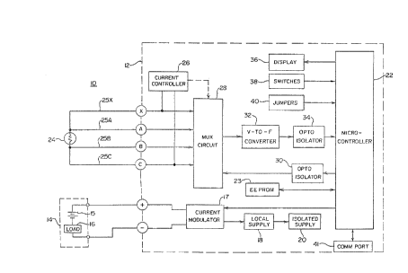
Figure 1 represents a general bloc~t diagram of the
preferred embodiment of the present invention. The
computerized remote resistance measurement system 10 of
the present invention includes a two-wire transmitter 12,
typically at a remote location, connected in series with
a power unit 14, typically at a central location. The
power unit 14 comprises a battery 15 connected in series
with a load 1&, both of which are connected in series
with a current modulator circuit 17 in the transmitter,
thus completing the two-wire current loop. The battery
15 is typically 24 volts DC, while the resistance of the
load 16 varies widely depending upon the application.
In the preferred embodiment, the current modulator
17 is configured to use the industry standard of 4-20 mA,
however, the former standard of 10-50 mA may also be
used. On the other hand, if the transmitter unit 12 is
centrally located, then the load 16 and the current
modulator 17 may be omitted such that the transmitter is
powered directly from the battery 15. Tn either case,
battery power is routed to a local power supply circuit
18, fram which power is routed to an isolated power
supply circuit 20. The local supply 18 provides power to
a microprocessor-based controller (microcontroller) 22,
' its associated electrically-erasable programmable read-
_a-
only memory (EEPROM) 23, and the associated display
circuitry, while the isolated supply 20 provides power to
the remaining transmitter circuitry. The local/isolated
supply arrangement will be described in more detail in
conjunction with Figure 5.
The transmitter 12 has four input sensor connection
terminals, X, A, B, and C, which are connected to an RTD
24 via connections wires 25X, 25A, 258, and 25C,
respectively, using a number of different sensor
configurations as will be seen below. One such input
configuration is shown in Figure 1, wherein a single
four-wire RTD 24 is connected 'to the transmitter 12. A
current controller circuit 26 powers the RTD 24 via the
current-carrying wires 25X and 25C connected to terminals
X and C, while terminals A and B are connected to measure
the voltage across the RTD 24 via 'the respective voltage
sensing wires 25A and 25B. In the general block diagram
of Figure 1, current would flow from the current
controller 26, out of the transmitter from terminal X,
through wire 25X and the RTD 24, and would return via
wire 25C to terminal C back to the current controller 26.
Although the invention is adapted to use a wide variety
of RTDs, i.e., having nominal resistances ranging from 10
ohms to 400D ohms, a typical RTD used with the present
invention is the widely available 10D ohm platinum bu7.b
type RTD. Moreover, many of the principles of the
present invention may also be used with other types of
condition sensors which vary their capacitance,
inductance, or magnetic fields in accordance with
temperature, position, liquid level, dielectric constant,
etc.
Each of the input terminals X, A, B, and C are also
connected to the inputs of a multiplexer circuit (MUX) 28
as shown. Since the voltage sensing terminals A and B
are connected to very high impedance inputs at the MUX,
practically ;no current flows into terminals A or B during
the measurement process. ~Ience, using the four-wire RTD
configuration shown, the voltage measured across
- 9 -
terminals A and B is the precise product of the
excitation current flowing from terminals X to C, and the
resistance of the RTD sensor 24. Hence, the resistance
of the current-carrying wires 25X and 25C connected to
terminals X and C do not enter into the resistance
equation. In this manner, lead-length compensation is
inherently being performed such that a much more accurate
resistance measurement can be obtained.
Multiplexing control signals are provided by the
microcontroller 22 to the MUX 2 8 via an optoisolator 30.
As will be explained in detail below, the multiplexer
circuit 28 provides the ability to individually select
any one of the RTD connection wires 25 in order to
measure, at the MUX output port, the voltage developed
from each of the input terminals X, A, B, and C to a
ground reference point. The output voltage signal of the
MUX 28 is connected to a voltage-to-frequency (V-to-F)
converter 32, which provides frequency output data to the
microcontroller 22 via another optoisolator 34. A
typical voltage-to-frequency converter, which could be
used as V-to-F converter 32, is disclosed in the 1990
Linear Applications Handbook, published by Linear
Technology, in Application Note 14, pg. 9.
Basically, the microcontroller performs the
functions of frequency-to-ohms conversion,
ohms-to-temperature conversion, and temperature-to-pulse-
width modulation (PWM) conversion to drive the current
modulator 17. The microcontroller 22 automatically
switches between a Measurement Mode, wherein the
resistance of the RTD is calculated and temperature
information is provided to the user, and a Test Mode,
wherein the microcontroller 22 directs the MUX 28 to
check if any of the wires 25 to RTD 24 are broken. In
the Measurement Mode, the MUX 28 provides voltage
information to the V-to-F converter 32, which, in turn,
provides frequency information to the microcontroller 22.
This frequency information, as well as information from
user-accessible mode switches 38 and a set of factory-
CA 02058591 1999-04-O1
- 10 -
programmed wire jumpers 40, is processed by the
microcontroller 22 to provide the temperature information
to the user via a visual display 36. The temperature
information is also transmitted over the two-wire link
via the current modulator 17. In the Test Mode, the
frequency information provided to the microcontroller 22
is used in conjunction with the addressing information
provided by the microcontroller 22 to the MUX 28 to check
for broken wires and to inform the user of precisely
which wire is broken via the display 36. A
communications test port 41 may also be connected to the
microcontroller 22 to allow for automated factory
calibration procedures. A Motorola 68HC05 is used as
microcontroller 22 in the preferred embodiment. The
EEPROM 23 is used to store calibration information used
in the system.
More specifically, in accordance with the operation
of the Test Mode, the microcontroller 22 directs the MUX
28 via optoisolator 30 to check whether any one of the
wires 25X, 25A, 25B, and 25C is broken, such that this
fault information is provided to the user via the display
36. As will be seen below, if wire 25X from the RTD 24
to terminal X is broken, or if wire 25C from the other
terminal of the RTD 24 to terminal C is broken, no
current will flow through the RTD. Even in the
Measurement Mode of operation, this condition will
immediately be noticed by the microcontroller 22 when it
receives either a zero frequency value or an over-range
frequency value from the optoisolator 34.
However, if one or more of the voltage sensing wires
25A or 25B from the RTD 24 to terminals A or B is broken,
current will still flow through the RTD device, and a
zero or over-range frequency value will not be detected
in the Measurement Mode. Moreover, since the input
terminal A or B would now be floating, one can not
predict what the voltage level out of the MUX will be.
If it remains within the approximate range of appropriate
voltage sensing values, the V-to-F converter 32 may
* Trade-Mark
~~~3~i~1
- 11 -
continue to output a nominal frequency value which
appears to be normal. Therefore, the present invention
implements the Test Mode to detect whether any of the RTD
connection wires, particularly the voltage sensing wires
25A and 25B) are faulty by connecting a known impedance
to the MUX output. Tf one of tale voltage sensing wires
25A or 25B is broken, the known impedance will load down
the outpwt of the MUX such that: either an over-range or
zero frequency value will be present at the input to the
microcontroller. Since the mic;rocontroller 22 is also
controlling the addressing to t:he MUX 28, the
microcontroller can determine exactly which wire is
broken and display this information to the user. The
following description provides a detailed explanation of
both the MUX circuitry involved and the saftware program
followed to perform this fault analysis.
Figure 2a is a simplified schematic diagram of one
embodiment of a multiplexing circuit/ 42 which serves as
the MUX 28 of Figure 1. The multiplexing circuit 42
includes a four-channel analog multiplexes 44, a current
source 46, a reference resistor RREF 48, and a known
impedance 52 switchably connected to the output Z of the
multiplexes 44 through a diode 50. In this embodiment,
three address lines, OPTO~, OPTO2, and OPT03, are provided
to the multiplexing circuit 42 from the microcontroller
22 via the optoisolator 30. As explained below, the
microcontroller 22 controls these address lines such that
the multiplexing circuit 42 connects any one of the four
input terminals X, A, B, or C to the multiplexes output
port Z, with and without switching in the known impedance
52.
As can be seen from Figure 2a, the current
controller 26 of Figure 1 basically comprises a constant
current source 46 and a reference resistor 48, labeled
RREF. The reference resistor RReF is used to precisely
determine the value of the current flowing through the
RTD sensor 24, labeled R~. Since the same current flows
~~~~~r~~
- 12 -
through the reference resistor 48 as through the RTD 24,
the current T through the RTD sensor R~ is:
{ 1 } I ' VR1IR1 ~ VREF~RREF
where VR~ is the voltage drop across R', and VREF is the
voltage drop across RREF ~ In the four-wire RTD
configuration shown, the voltage drop across R~ is equal
to the voltage measured at terminal A to ground minus the
voltage measured at terminal B to ground, i.e., VR~ = Vp-
Vg. Similarly, the voltage drop across RReF is equal to
the voltage measured at terminal C to ground, i.e.,
REF - Vc° Hence,
{2 } R9 '_' vRi~I ' vRl~ LVREF~RREF~ r ar
{3} R) _ ~Vp°Vg)~(Vc~RREF}, and finally
{4} R~ - L LVp°Vg~~VE~RREF°
If a two-wire RTD sensor were used such that there were
no connection wires from R~ to terminals A or B, then
{5} R~ - L ~Vx-V~~~V~~RREFr
although no lead-length compensation would be performed.
In other words, using a two-wire RTD sensor, the sensor
resistance is proportional to Vx-Vc. When using a faur
wire sensor, the sensor resistance is proportional to Vp-
Vg. If a three-wire RTD configuration were used, wherein
no connection wire exists from R1 to terminal B, the RTD
sensor resistance would be proportional to Vp-Vc~ and a
different calculation would be performed to compensate
for lead length. Tn any case, note that the excitation
current I provided by the current source 46 is na longer
part of the resistance equation, since the final
resistance equation is a function of ratios of voltage
values. As will be explained below, the microcantroller
22 utilizes these proportional voltage values to
calculate the resistance of the RTD sensor 24 in the
Measurement Mode. In the Test Mode, the known impedance
52 is switched in, such that the measured value of the
RTD sensor is now being affected by the resistance of the
known impedance connected in parallel.
Figure 2b illustrates representative waveforms for
the address lines OPTO~, OPTO2, and OPT03 from the
_ 13 _
optoisolator 30. Using these waveforms, the operation of
the multiplexing circuitry 42 of Figure 2a will now be
described. As illustrated in the waveform diagram, a
complete measurement cycle is comprised of a Measurement
Mode and a Test Mode. During the Measurement Mode, the
multiplexes address line OPTO3 always remains low, while
it remains high through much of the Test Mode. With a
low voltage from OPTO3 applied to the resistor 52, the
diode 50 is reversed biased, such that the known
impedance has no effect on the measurement of the output
voltage at Z.
At time ty, the microcontroller 22 places a high
voltage level on address line OPTO~, while OPTOz and OPT03
remain low. Since OPTO~ is connected to multiplexes
address port ao, and since OPTOZ is connected to address
port a~, a binary '01' is applied to the multiplexes 44
such that multiplexes data post d~ is connected to the
output port Z. Hence, at this time, the voltage level at
the output port Z of the multiplexes 44 represents the
voltage level apparent at input terminal B as measured
from ground. This is shown as Z = D at the bottom of
Figure 2b during the time interval t~~t2. At time tz, the
address line OPTOZ goes high, such that a binary °11' is
applied to the multiplexes 44. Accordingly, the
multiplexes selects its data port d3 such that the voltage
level at output post Z is equal to that of the input
terminal X, i.e., Z = X. At time t~, a binary '10° is
used to address multiplexes data port dz, such that Z = A.
Finally, at time t4, a binary '00' is used to address
multiplexes data port do such that Z = C. Accordingly,
all four input terminals X, A, B and C have been
individually selected during the Measurement Mode.
In the Test Mode at time t6, address line OPT03 goes
high, such that resistor 52 is now connected to the
output port Z at 45 through the forward-biased diode 50.
Note that the diode 50 is serving the purpase of a
switch, under the control of the address line OPT03, which
connects a known impedance, resistor 52, to the
~~a~~~~.
- 14 -
multiplexes output port Z. Since the resistor 52 is now
in the circuit, 'the voltage output at port Z is now
proportional to the resistance measurement a~t terminal B
made in parallel with the resi:>tance of the known
impedance 52. This is indicatE:d at the bottom of
Figure 2b as B+ (terminal B "plus" resistor 52) measured
during time interval tb-tT. Similarly, during time
interval t7 t8, X+ is being mea;aured. Resistance values
A+ and C+ are then measured during time intervals t~--t9,
and t9-too, respectively.
In the preferred embodiment, the value of resistor
52 is 1,000,000 ohms. This value is much higher than the
normal operating range of resistance values of the RTD,
nominally 100 ohms, while it is much lower than the
potentially infinite resistance value seen at the output
of the multiplexes 44 if a wire is broken on the selected
input port. In other words, in the Test Mode, the
presence of the known impedance 52 would not
significantly affect the voltage level at the output port
Z when all the wires are connected to a relatively low-
impedance RTD. However, if one of the wires is broken,
the presence of the known impedance 52 will cause the
output voltage level to drastically change, or rise in
this case, if one of the RTD input connection wires is
broken. Hence, if one of the connection wires 25 is
broken such that ane of the multiplexes inputs is open,
the measured resistance value for that selected terminal
will approximate that of resistor 52. Accordingly, if a
multiplexes input is open, the frequency output of the
V-to-F converter 32 will not be within a nominal RTD
range when that particular multiplexes channel is
addressed. Since the microcontroller 22 is controlling
the address lines OPTO~, OPTOz, and OPTO3, the
microcontrol:Ler knows exactly which multiplexes input
terminal X, A, B, or C is being addressed. Hen;.e, the
microcontrol:Ler can determine exactly which wire is
broken, and :indicate this information to the user via the
display 36.
~~~8~~~.
Figure 3a is an alternate embodiment of the
multiplexing circuitry of Figure 2a, which has been
modified to utilize only two address lines. In the
multiplexing circuit 54 of Figure 3a, the third address
5 line OPT03 has been eliminated through the addition of a
D-type flip-flop 56. Address line OPTO~ is connected to
the clock input, and address line OPTOZ is connected to
the D input, respectively, of 'the D-flip-flop 56. The
flip-flop output Q is connected to the resistor 52. If
10 the D input is high, the Q output will go high on the
next rising edge of the input clock waveform. Hence, the
phase relationship between address lines OPT01 and OPTOz
. are used to determine the state of 'the D-flip-flop output
Q, which now functions as the third address line OPTO3.
15 Referring now to Figure 3b, the operation of the
multiplexing circuitry 54 of Figure 3a will be described.
During the Measurement Mode, the multiplexer address line
OPTO~ always rises before the address line OPTOz such that
the Q output of the flip-flop 56 remains low. With a low
output Q, the diode 50 remains reversed biased, such that
the known impedance 52 has no effect on the measurement
of the voltage at output port Z. hence, as shown at the
bottom of Figure 3b, the output port Z represents the
resistance at terminals B, X, A and C, respectively.
However, note that the address line OPTOz remains
high at time t6, such that the Q output goes high upon the
rising edge of OPTO~. Therefore, during time interval tb-
t7, the parallel combination of the resistance seen at
input terminal X plus resistor 52, or X+, is being
measured. Similarly, during time intervals t~ ts, t$-t9,
and t9 too, resistance values B+, A+, and C+,
respectively, are measured in the Test Mode.
Figure 4a is another simplified schematic diagram
for the multiplexing circuit 28 of Figure 1, wherein an
additional multiplexed input, terminal D, is utilized to
more accurately determine the value of the reference
resistor RREF° Note that the input terminal D is internal
to the transmitter unit. Also note that an additional
16
address line is required to select the additional input
terminal D.
In multiplexing circuit 58, the reference resistor
62 is connected between input terminals C and D of the
multiplexer 60, and is not directly connected to ground
as before. Instead, a current return resistor RRer 64 z's
connected between input terminal D and ground as shown.
In this way, the current from i~he current source 46 flows
through the RTD 24, the reference resistor 62, and the
return resistor 64, to ground. Instead of measuring the
voltage V~ to ground in order to determine the value of
the reference resistor RR~F, two voltage measurements, V
to ground and Vp to ground, are made such that the value
of the reference resistor RREF iS proportional to V~-Vp.
The use of this fifth internal terminal D allows the
measurement of the reference resistor RReF t° be
completely differential, i.e., V~-Vp, such that voltage
offsets no longer affect the accuracy of the measurement.
Hence, operational amplifiers may be used in the current
source 46 which do not have a necessarily low offset
differential specification. Since input bias and offset
currents are no longer at issue, the circuit has
substantially no hero or Span error, except for the
temperature coefficient of the reference resistor 62.
The effect of any noise on the ground lines is also
significantly reduced. In other words, in using this
fifth input terminal configuration, a much more accurate
determination of the reference resistor R~~F can be
achieved.
In order to measure the voltage VD at the additional
input terminal D, an additional data port is required on
the multiplexer. As shown in Figure 4a, a five-channel
analog multiplexer 60 is controlled by three address
lines ao, a~, and a2, which are connected to OPTO~, OPTOZ,
and OPT03, respectively. A fourth address line OPT04 is
connected to the known impedance 52 as shown.
Referring now to Figure 4b, representative
addressing waveforms for the operation of the
~O~i~~~~.
- 17 -
multiplexing circuit 58 of Figure 4a are shown. In the
Measurement Mode, the fourth address line O:PTO~ remains
low, such that the other three address lines OPTO~, OPTOZ,
arid OPT03 control the selection of the input terminal
voltage which is applied to thsa output port Z. For
example, during time interval t~-t2, a binary °001' is
applied to the multiplexer 60, such that data port d~ is
selected, whereby the voltage at input terminal C is
connected to output port Z. Again, this is shown at the
bottom of Figure 4b as Z = G. During time interval tz-t3,
a binary '011' is used to select multiplexer data port d~,
such that Z = A. Similarly, input terminals B, D, and X
axe selected in accordance with the waveforms shown. At
time tl, the fourth address line OPT04 goes high in the
Test Mode such that the known impedance 52 is switched
into the circuit. Again, a binary '001' address is sent
by the microcontroller to select input terminal C, such
that Z = C+. A similar addressing scheme is used to
select A+, B+, D+, and X+ as shown.
Figure 5 is a detailed schematic diagram of 'the
preferred embodiment of the MUX 28 of Figure 1, wherein
five multiplexed inputs are controlled by only two
address lines. In multiplexing circuit 70, the four
external input terminals X, A, B and C, have been
reversed from the previous figures to more accurately
illustrate the operation of the current controller
circuitry and the isolated power supply circuitry. As
before, the two address lines OPTO1 and OPT02 from the
microcontroller 22 serve to control the four-channel
analog multiplexer 72 via the optoisolator 30, and this
circuitry operates substantially as explained above.
However, an additional two-channel analog multiplexer 74
is used to multiplex the internal input terminal D with
the output port Z, of the multiplexer 72, and thereby
provide the output port Z3 as the input to the
voltage-to-frequency converter 32 of Figure 1. Another
difference in Figure 5 from the previous circuit is that
another two-channel analog multiplexer 76 is used as an
- 18
electronic switch to perform the function of the diode
50, i.e., to control the switching of the known impedance
in the Test Mode. Finally, note that a D-type flip--flop
80 is again used to eliminate the need for the third
address line, and a diode-OR circuit is used to eliminate
the need for the fourth address line.
The circuitry in 'the upper-left portion of Figure 5
performs the function of the current controller 26 of
Figure 1. An operational amplifier 82, powered from a
split voltage supply V-~/V-, is used to sink current
returning into the transmitter input terminal X to supply
V- through a resistor 84. A resistor 86, which functions
_ as the reference resistor RREF, provides a sOUrce Of
current from V-~ at input terminal D to the RTD via. input
terminal C. A resistor 88, also connected to terminal D,
performs the function of the current return resistor RR~T.
Biasing resistor 90 and feedback capacitor 92 serve their
normal functions in the op-amp current source circuit.
In the preferred embodiment, two aptoisolators 94
and 96 are used to generate the two address lines OPTO~
and OPTO2, as shown in the bottom-left portion of
Figure 5. The output ports from the microcontroller 22
are isolated from the address lines such that the RTD
sensor can be connected to a ground reference point which
may be hundreds of volts different from the ground of the
two-wire transmitter, without the risk of a shock hazard
or a malfunction. In tine preferred embodiment, an
investor circuit, comprised of a resistor 98 and a
Schottky NAND gate 100, are used to improve the switching
waveform for the clock line to the flip-flop 80, since
the optoisolator has a slow turn-off time.
As described above ::m accordance with. Figure 3a, the
output ~ of the D-type flip-flop 80 is used as the third
address line, i.e., the Test Mode line, to address the
analog multiplexes 76 via its address part ax. The known
impedance, i.e., a resistor 102, is connected from 'the
output port Z1 of the multiplexes 72 to the output port Zz
of the multiplexes 76 as shown. When the Q output of the
- 19 -
flip-flop is low, a zero is applied to the ax address
port, such that the multiplexes data port do is selected.
This connects the outpwt Z1 of 'the multiplexes 72 to the
output ZZ of the multiplexes 76, effectively shorting-out
the resistor 102 such that the known impedance is not in
the circuit. In the Test Modes however, the Q output
goes high, such that the resistor 102 is connected to the
positive supply voltage V+ at multiplexes data port d~,
thus connecting the resistor 102 into the circuit.
In either case, the output ZT of the multiplexes 72
is connected to the data port d~ of the mul~tiplexer 74.
The internal input terminal D, which is used to measure
the voltage across the reference resistor 86, is
connected to the other multiplexes data port do. Still
another address line, aY, is used to switch between data
ports do and d~ to provide the output Z3 to the V-to-F
converter 32. The address line aY is controlled by a
combination of the address lines OPT01 and OPTOZ, and the
inverted-Q output of the flip-flop 80, all configured as
an OR gate through diodes 104, 106, and 108, and a pull-
down resistor 109, as shown. Hence, whenever OPTO~ or
OPT02 or inverted-Q is high, the address port aY will be
high, and the output port Z~ will be connected to the
output Z3 through the multiplexes 74. Switching waveforms
will be shown below for the various input configurations.
As shown in the bottom-right portion of Figure 5,
the isolated power supply circuit 20 of Figure 1 is
comprised of a transformer 110 and several other standard
components as shown. A DC-to-AC converter in the local
supply 18 provides AC to the transformer 110. The
isolated AC voltage is then rectified, filtered, and
split into two regulated supplies such that V+ is
approximately 2.5 volts DC above the ground reference
112, and V- is approximately 2.5 volts DC below the
ground reference 112. Numerous other isolated supply
configurations may also be used.
The following part numbers and values are
representative of those used in the preferred embodiment:
~0~~~~~.
- 20 -
Component T~ a Value
Multiplexes 7~ CD 4052
Multiplexers 74,76 CD 4053
D flap-flop 80 CD 4013
Op-amp 82 TLC27L7
RaeF 86 301 ohm, 1%, 5ppm/°C
RREr 88 100 ohm
R84 499 ohm
R90 lOK ohm
R98 100K ohm
8102 1 Meg ohm
8109 1 Meg ohm
~f couxse, other component types and values may be used
for different applicatians or other circuit
configurations.
Figure 6a is a schematic diagram illustrating the
input circuit configuration for the multiplexes of
Figure 5 when a two-wire RTD sensor is used without lead-
length compensation. The RTD 24 is connected via two
connection wires 25X, 25C, to the input terminals X, C,
of the multiplexes 72 of Figure 5. The excitation
current I flows from V+, through RRET 88 to terminal D,
through RREF 86, out of terminal C, through R1, into
terminal X, through current source 46, and back to V-.
Note that while the direction of the current source 46
and the polarity of the supply voltages V+, V-, remain
the same as that of Figure 5, resistor 90 and the op amp
82 have been omitted for purposes of simplification.
Also note that the input terminal X is connected to
multiplexes data port do as shown in Figure 5, as opposed
to being connected to the higher-order data ports d3 or d4
as was the case for the figures previous to Figure 5.
As will be explained in mare detail in the flowchart
below, the frequency values corresponding to the voltages
at input terminals A, B, C, D, and X are measured as
required for the particular input sensor configuration.
Each value is read for approximately 300 milliseconds
(ms). A table of the five most recent frequency values
is kept for each input terminal. The five values are
averaged, calibrated to correct the voltage-to-frequency
conversion, scaled to account for any voltage-to-
frequency converter drift, and then used in the
- 21 -
resistance formula for the particular input sensor
configuration. The resulting .resistance value is
corrected for calibration errors, converted to
temperature utilizing either a table of resistance-
temperature values or a polynomial equation, arid
linearized using the particular temperature coefficient
for the input sensor. The final 'temperature value is
then saved. If a multi-sensor configuration is used, the
various linearized temperature values may be combined to
form a differential temperature measurement.
In the two-wire single-sensor configuration
illustrated in Figure 5a, the resistance formula is:
° (6) R1 = C (~x-V~)/ (V~-Vp) I~REF~
and the value Vx is °termed the most acta.ve variable, since
its value changes more often than the other variables.
This is due to the fact that the current T through the
circuit is essentially constant, so that V~ and Vp change
very little. since R~ changes with temperature, VX also
changes with temperature. Accordingly, input terminal X,
which corresponds to the most active variable Vx, is
usually read by the microcontroller more often than the
other variables.
Now referring to Figure 6b, a waveform timing
diagram for the operation of the circuit of Figure 5 is
shown when used with the input configuration of
Figure 6a. The timing diagram illustrates the two
address lines OPTO~ and OPTOZ as seen at the address ports
ap and a1 of the multiplexes 72. Hence, OPTO~ and OPTOZ
control the multiplexing of the four input terminals X,
A, B, and C. The third waveform, labeled Q, represents
the voltage level at the output Q of the flip-flop 80,
which is connected to address port ax of the multiplexes
7C,. Therefore, the waveform Q represents the control
signal for the switch that connects °the resistor 102 into
the circuit for the Test Mode. The fourth waveform,
labeled ay, represents the logical OR of OPTO~, OPTOz and
the inverted-Q output of the flip-flop 80, as seen at the
address port aY of the multiplexes 74. Hence, this
- 22. -
address port aY effectively represents the third address
line for multiplexing the fifth input terminal D.
Finally, the designation Z3 at the bottom of Figure 6b
represents the output port of the multiplexes 74. The Z3
waveform illustrated which input terminal is being
individually selected by the multiplexing circuit 70 of
Figure 5 during particular time intervals. Note that in
using the two-wire RTD sensor configuration, there is no
Test Mode per se. If the connection wire 25X to input
terminal X was broken, the voltage at input terminal X
would approximate V-, such that the rnicrocontroller would
read the frequency output of the V-to-F converter to be
. an over-range value. Similarly, if the connection wire
25C to input terminal C was broken, the voltage at
terminal C would approximate that of V+, such that the
frequency output of the V-to-F converter would be zero,
or under-range.
At time t~ of Figure 6b, the microcontroller directs
address line OPTO~ to go high. Since OPTOy is connected
as the clock line of the flip-flop 80, and since OPTOZ is
low at this time, the flip-flop is cleared such that the
Q output remains low. Address line OPTO~ remains high for
approximately 150 microseconds (us) and goes low at time
t2. The microcontroller does not measure any parameters
during time interval t~-t2, so nothing is shown for the Z3
output.
During the time interval tz-t3, a binary °00' address
is applied to the multiplexes 72 such that data port do is
selected. Accordingly, the voltage value from input
terminal X to ground is seen at the multiplexes output Z~.
Since the flip-flop output Q is low, data port do of the
multiplexes 76 is selected such that resistor 102 is out
of the circuit. Finally, since the address line ay is
high during this tame interval, data port d' of the
multiplexes 74 is selected as the output Z3 to the V-to-F
converter 32. As can be seen at the bottom of Figure 6b,
the output Z3 represents the value of terminal X during
the time interval t2-t3. Tn the preferred embodiment,
~O~~~J1
- 23 _ z
this time interval t2-t3, used far reading input terminal
X, is appraximately 300 ms.
At time t3, OPTO~ goes high, and 150 ACS later at time
t4, OPTOZ goes high, such that a binary '11' is applied to
the multiplexes 72. The address line OPTO~ must go high
before OPTOZ in order to ensure: that the Q output of the
flip-flop remains low. During the time interval t4-ts,
the voltage at the input terminal C to ground is seen at
output Z3. Again, input terminal C is being read by the
microcomputer for approximately 30o ms.
At time t~, both OPTO~ and OPTOZ go low, such that
the input terminal X is again being read by the
microcomputer. As explained above, terminal X represents
the most active variable, and, accordingly, this value is
updated twice per measurement cycle.
At time t6, OPTOZ goes high, such that the Q output
of the flip-flop goes high caith the rising edge of OPTO~
at time t~. Again, the time interval needed to ensure
that the flip-flop is set, i.e., the time interval t6-t~,
is an the order of 150 ~,s. Once, the Q autput is latched
high, the address line OPTO~ can go low at time t8 such
that the address line aY can also go low. Accordingly,
during the time interval t8-t~, input terminal D is being
read as the output Z~ of the circuit. At time t~, OPTO~
is again set high such that the flip-flap is clocked with
OPTOZ low. Hence, the Q output is reset law, the address
line ay is reset high, and the next measurement cycle
begins.
Figure 7a is a schematic diagram illustrating the
input configuration for. the multiplexes of Figure 5 when
a four-wire RTD sensor is used. The four-wire sensor
configuration of Figure 7a differs fram the twa-wise
configuration of Figure 6b in that a third wire 25A and a
fourth wise 25B are used as voltage sensing wires
connected to the multiplexes 72. Using this foul-wire
RTD configuration, the resistance of the RTD is
calculated using the following ec{uation:
7 J R~ - L Wp'Vg ~ I ~ Ug-'Up ~ J RREF °
~~!~~ ~~1
In this configuration, V~ is 'the most active variable far
RTD measurement, since Ve, V~, and Vp change very slowly
if at all, while VA varies directly with the sensoros
resistance. Note that Vx is as active as Va, although it
is not used in the resistance equation. Hence, in the
preferred embodiment, input terminal A is updated
approximately three times per second, and input terminals
A and B are checked for broken wires approximately every
two seconds.
Note that only terminals A and B need to be checked
by the microcontroller for broken wires in the Test Mode,
since a break in any other wires will be detected in the
. normal Measurement Mode. In other words, if terminal X
is open, then the voltage Vx at terminal X will
approximate V-, while VA, V8, and V~ will all equal V+.
Accordingly, the microprocessor will sae an over--range
frequency value for X, while a zero frequency value for
A, B, and C. This condition indicates that terminal X is
open. Similarly, if terminal C is open, then Vx, VA, and
VB will all approximate V- and produce an over°range
frequency value, while V~ will be at V+ and therefore zero
Hertz. In the Test Mode, if the voltage sensing wire 25A
to terminal A is open, then VA will be at an unknown
voltage value at a high impedance, such that the voltage
for A+, i.e., the parallel combination of the A terminal
impedance and the known impedance connected to V+, will
be equal to V+. If terminal A were not open, then th-e
low impedance on terminal A would cause the parallel
combination to be within range or low. The same result
would occur for B+ if terminal B were open. Tn other
words, an open wire to terminals A or B will correspond
to zero frequency for A+ or B+.
Figure 7b illustrates the timing waveforms for the
four-wire RTD sensor configuration of Figure 7a. Note
that portions of the Test Mode are interleaved with
portions of the Measurement Mode in order to more
efficiently perform the functions of both modes. At time
t~, the rising edge of OPTO~, when OPTOZ is low, ensures
~~~c~W~.
_ 25
that the Q output remains low and the address line ay
remains high. During time interval t~--tz, a binary '01'
is applied to the multiplexes 72, such that 'the data port
d~ is connected to output post L~ for reading the voltage
at input terminal A. Since the Q output is low, the
multiplexes circuit 70 remains in the Measurement Mode,
and the resistor 102 is out of the circuit. During time
interval tz-t3, a ba.nary ' 10' is applied to the
multiplexes 72, such that input terminal B is being seed.
Each of the these time intervals is approximately 300 ms.
At time t3, OPT02 goes low to ensure 'that the rising
edge of OPTO~ at time t'~ does not set the Q output high.
Time interval t3-tG is approximately 4 ms, to prevent a
slow fall time on OPTO2, i.e., slower than the rise time
of OPTO~, from allowing the circuit to go into the Test
Mode. As a result, input terminal A, representing the
most active variable, is again read for approximately 300
ms during time interval t4-t5. Input terminal C is read
during time interval ts-tb, and input terminal A is again
lead during time interval ta-t7.
At time t~, OPTO~ goes high in order to latch the Q
output high with the rising edge of OPTO~ at time ta.
Time interval t~-ts, in the preferred embodiment, is
approximately 4 ms in length, which is sufficient time to
prevent a slow fall time on OPTO~ from improperly
affecting the operation of the circuit. Even though the
Q output is high during the time interval t~°t~o, the
address line ay is low, such that input terminal D is
being lead during the Measurement Mode. During time
interval ~t~o-t», the value of the A input terminal is
again updated. At time t9~, OPTOZ goes high such that the
Q output goes high 150 ACS later with the rising edge of
OPTO1 at time t~2.
At time t~3, OPT02 goes low, and the Test Mode is
entered in order to detect a broken wire at input
terminal A. As can be seen from the waveforms, a binary
'01' is applied to the multiplexes 72, such that the data
post d~ is connected to the output port Z~. Since the Q
~~ar3~~~.
-- 26 -
output is high, data port d~ of the multiplexer 76 is
connected to its output ZZ, such that 'the lower end of
resister 102 is connected to V+. Hence, terminal A, plus
the known impedance, is being read as the value at the
output port Z3, i.e., Z~ = A+.
At the end of the 4 ms tame interval t~4-tls, the Q
output is reset such that the input terminal A can be
again be measured in the Measurement Mode during time
interval t~s--tab. During tame intervals tab--t~8, the Q
output is again set high, and input terminal B is
selected such that the value of B-E can be measured in the
Test Mode during the time interval t1n-~t19. Finally, OQTOZ
goes low at time t~9 such that the Q output is reset at
time t~, and the measurement cycle is again restarted.
Figure 8a is a schematic diagram illustrating the
input configuration for the multaplexer of Figure 5 using
a three-wire RTD sensor configuration. As can be seen
from the figure, only one voltage sensing line 25A is
used an this embodiment. Accordingly, the RTD resistance
calculation formula as:
t87 R~ ' ~ ~ ~Vp-V~)"(Vx'VA) )~(V~-Vp) JRREF~ or
R~ _ ~ ~2vp-Vp-'~X~~t~C-vp~ ~RREF'
Again, A is the most active variable because C and D are
relatively stable, and x is as active as A. Note that
only terminal A needs to be checked during the Test Mode.
If terminal x is open, then the variable X will be over-
range and A and C will be zero Hertz. If terminal C is
open, then x and A will be over--range, and C will be zero
Hertz.
The taming waveforms for the three-wire sensor
configuration of Figure 8a are shown in Figure 8b. The
operation of the circuit of Figure 5 with the three-wire
RTD configuration is similar to that of the previous two
figures, except that the sequence of variables read into
the microcontroller are different, as shown at the bottom
of Figure 8b as Z3. Again, each Measurement Mode or Test
Mode input terminal reading period is approximately 300
ms, while time intervals tb tl, t1o-t~l, and tt3-tt are
- 27 -- _
approximately 4 ms. Time intervals t7-t8 and t~~-t12 are
apgroximately 150 ~.s.
Figure 9a is a schematic diagram illustrating the
input configuration for the multiplexer of Figure 5
having a three-wire dual-RTD ss:nsor configuration using
no lead-length compensation, Two RTDs are often used for
differential temperature measug~ements. However, in all
prior two-wire transmitter systems, a true differential
temperature measurement is not possible. Tn the
preferred embodiment, however, the resistance values of
each RTD sensor R~, RZ are individually calculated such
that a true differential temperature measurement can be
. made. Accordingly, the resistance formulas used with the
three-wire dual-RTD input configuration are as follows:
{10) R~ = L ~vX-vp)I(v~-vp) 7RREF~ and
{ 11 } RZ - ( ~ Vp-v~ ) ~ W~-Up ) J RRE F .
As before, only the input terminal A needs to be checked
in the Test Mode, since if the wire 25X to terminal X
were broken, the X frequency value would be over-range
and the A and C frequency values would be zero Hertz.
Similarly, if the wire 25C to terminal C were broken,
then the X and A frequency values would be over-range,
and the C frequency value would be zero Hertz.
Figure 9b illustrates the timing waveforms for the
input configuration of Figure 9a. From the waveforms, it
can be seen that terminals A, C, X, A, and X are first
measured in the Measurement Mode, then terminal A plus
the known resistance 102 is measured during time interval
t8 t9 in the Test Mode. Finally, terminal D is measured
in the Measurement Mode during time interval t9-t9.
Figure l0a is a schematic diagram illustrating the
input configuration for the multiplexer of Figure 5
having a five-wire dual-RTD sensor configuration
utilizing lead-length compensation. This five-wire dual-
RTD input configuration utilizes connection wire 25B to
compensate for the other lead lengths. The resistance
formulas, however, become rather complicated:
~~zi~ i~~.
2g
12 ) R~ - I C WX'"Vp~ -2 ~Vg°'~C~ J' ~V~-Vp~ JRREF~ and
13 } Rz - C C ~Vp-'Ug~ '_ tVg°UC~ ~ ~ ~V~°vp~ ~RREF'
Terminals X and A represent the most active variables.
Both terminals A and B are checked in the Test Made. If
wire 25X to terminal X or wire 25A?. to terminal A is
open, such that R~ is open, the microcontroller will
receive an over-range frequency value for X and a zero
frequency value for A, B, and C. If wire 25A2 to
terminal A is open, or R~ is open, then the controller
will receive an over-range frequency value when reading
terminals A and X, and a zero frequency value for
terminals B and C in the Measurement Mode. If wire 25B
to terminal B is open, a zero frequency value wil:1 be
received for B+ in the Test Mode. Finally, if wire 25C
is open, then terminals X, A, and B will be over-range
frequency values and terminal C will be a zero frec~.iency
value in the Measurement Mode.
From the timing waveform illustrated in Figure 10b,
it can be seen that the five-wire dual-sensor
configuration of Figure 10a only utilizes the Test Mode
during time intervals t~~-t~2 arid t~2-t~3. During the other
times, terminals A, B, C, D, and X are measured as shown.
Figure 11a is a schematic diagram illustrating the
input configuration for the multiplexer of Figure 5
having a three-RTD input configuration. No lead-length
compensation is being performed. The resistance formulas
are:
14 } R~ - ~ ~Vx°Vp~ ~ w~'-Vp~ ~RREF ~
15~ RZ - C Wp°Vg~ ~ ~~p-~p~ ~~EF' and
{is~ R3 - C LVg-~p~I ~V~-Vp~ ~RREF°
Terminals X, A, and B represent the most active
variables. If wire 25X is open, the frequency value for
X will be over-range, and that of A, B, and C will be
zero. If wire 25A is open, then A+ will be zero in the
Test Mode. Similarly, for wire 258, B+ will be zero in
the Test Mode. If wire 25C is open, then X, A, and B
will over-range and C will be zero in the Measurement
Mode.
~~~a~~~.
_ 2g _
As before, Figure 11b illustrates the corresponding
timing waveforms for the three-RTn input configuration
shown above. In the Measurement Mode, the variables A,
C, B, X, A, X, and B are read before A+ and B+ are
measured in the Test Mode. Finally, the D variable is
measured in the Measurement Mode. Note that the
multiplexing scheme of Figure 11a includes the ability to
independently measure the value of three different
temperature sensors, and to compute the average of the
three temperature sensors in the microcontroller.
However, no lead-length compensation is being performed.
Figure 12 is a flowchart illustrating the specific
sequence of operations performed by the microcontroller
of Figure 1, as used with the multiplexing circuitry 70
of Figure 5, in accordance with the practice of the
preferred embodiment of the present invention. Beginning
with the start step 510, the microcontroller 22 is
initialized at step S12 by a hardware reset or power-up
reset. The initialization step also includes diagnostic
tests, and hardware arid software setup, e.g., clearing
memory, initializing variables, etc. The interrupts are
initialized at step 514. As will be seen below, the
microcontroller utilizes a interrupt-driven programming
routine, wherein the main measurement cycle, comprised of
steps S16-528, are temporarily halted upon the occurrence
of an interrupt. Note that the interrupts can occur any
time during the main measurement cycle.
Referring momentarily to Figure 13, the various
interrupt operations per:~ormed by the microcontroller are
illustrated. At input capture interrupt step T10, the
input frequencies for the input terminals A, B, C, D, X,
A+, or B+ are captured. As explained above, the measured
voltage levels at these input terminals are multiplexed
by the MUX circuit 28 and are applied to the voltage-to-
frequency converter 32 'to convert the levels into digital
pulses. These frequency pulses are applied through the
optoisolator 34 to the microcontroller 22, wherein an
interrupt is generated for each pulse. The input capture
- 30 -
interrupt routine I10 increments the number of pulses
counted per cycle, (i.e., "counts"), saves 'the system
clock time for the first pulse of the cycle ("old
clock"), and updates the latest pulse time signature
("new clock") until a new cycle: is started at the end of
a 300 ms measurement cycle. A timing module saves the
accumulated clocks and counts as the measured input value
~A,B,X,A+,B+). For points C and D this value is the
latest of a set of eight readings for the measured value
of the C or D input variables.
Now referring back to step S16 of Figure 12, the RTD
resistance is computed using the information from the
. input capture interrupt routine I10. The clocks and
count information for each input terminal are selected
for the 300 ms measurement duration, whereby the next
input terminal in 'the sequence is measured. After 300 ms
of capturing time, the old and new clock values are
subtracted and saved with their number of accumulated
counts or pulses. The capture variables are then reset,
and the hardware is switched to measure the next input
terminal. The captured cloaks and counts are then limit
checked. If these values would correspondence to
frequencies greater than 850 Hertz or less then 10 Hertz,
a fault indication is provided to the user via the
display 36. Otherwise, the inputs for A, B, and X are
scaled to ohms. The eight most recent values for input
terminals C or D are averaged and scaled to form data
points representative of the resistances at the input
terminals. The data points are then combined using the
aforementioned resistance formulas described above. A
raw resistance value for each RTD sensor is then stored
in RAM.
In step 518, the raw resistance value is linearized
by applying factors from a linearization error table to
the raw resistance values for R~, RZ and/or,R3. The
linearization error table is comprised of empirically-
determined coefficients for linearizing the resistance-
verses-temperature curve of each RTD as a function of
1 ~~~~i~~~
measured voltage across the RTD. Linearization tables
are known in the art. Moreover, linearization may not
required for certain types of condition sensors.
Depending upon the input ;sensor configuration, the
linearized RTD values may then be combined and stored as
a combined result. Similarly, the linearized resistance
values may be subtracted and the difference between two
RTDs stored, or the average of two or three sensors may
be computed. In the prior art, the differential
IO resistance between RTDs would :be measured, assuming each
resistor temperature coefficient is linear. This is not
a correct assumption, particularly if a wide range of
temperatures are measured. Hence, the present invention
permits linearization in software for each RTD
independently of each other. Note that in the multi-RTD
sensor configurations shown in Figure 9a, 10a, and 11a,
each of the individual RTD sensors can be linearized
individually before being compared to the other RTD to
determine the differential or average temperature
measurement.
In step S20 the microcontroller tests for broken
wires, i.e., open connections at the input terminals.
For broken wire testing, only the latest result for the
measured values of X, A, B, C, D, A+, and B+ (as
required) is used. As explained above, the broken wire
test analysis is different for each of the input sensor
configurations described above. Table 1 provides a
summary of the broken wire analysis performed by the
microcontroller 22.
_-____________________.._TABLE
1-____________~____________
For 2-wire sensors (Figure 6a)
Condition: Error:
X = OVER-RANGE and C ZERO R~ = open
=
For 4-wire sensors (Figure 7a)
Condition: Error:
A & B & C = ZERO and = OVER-RANGE X = open
X
A+ = ZERO A = open
B+ = ZERO B = open
A & B & X = OVER~RANGE and C = ZERO C = open
- 32 -
For 3-wire sensors (Figure
Sa)
Condition: Error:
X OVER-RANGE and A & C = ZERO X = open
=
A+ = ZERO A = open
X A = OVER-RANGE and C - ZERO C = open
&
For dual sensors w/out compensation
(Figure 9a)
Condition: Error:
A C = ZERO and X = OVER-RANG1:.R~ = open
&
X A = OVER-RANGE and C = ZERO RZ = open
&
A+ = ZERO A = open
For dual sensors w/compensation(Figure l0a)
Condition: Error:
A B & C = ZERO and X = OVERIdANGER~ = open
&
X A = OVER-RANGE and B & C = RZ = open
& ZERO
A B & X = OVER-RANGE and C = C = open
& ZERO
A+ = ZERO A = open
B+ = ZERO B = open
For triple sensors (Figure
11a)
Conditian: Error:
A B & C = ZERO and X = OVER-RANGER~ = open
&
X A = OVER-RANGE and B & C = Rz = open
& ZERO
A B & X = OVER-RANGE and C = R3 = open
& ZERO
A+ = ZERO A = open
B+ = ZERO B = open
___ ___________________________________________-__________
In step S22 of Figure 12, the microcontroller
processes the duty cycle information, i.e., it converts
the linearized RTD values into duty cycle information.
Every 300 ms, the linearized RTD values are converted
into a desired duty cycle parameter for pulse-width
modulation of the current modulator 17 shown in Figure ~..
The duty cycle is expressed as a percentage of on-time
verses off-time. The duty cycle is calculated from the
linearized RTD values by applying a combination of
calibration, ranging, and trim factors in accordance with
the following formula:
{17} DTON = CT4 + {[(RTDLIN ° RZERO)/2]/RSPAN}TONSP
wherein DTON is a desired on-time value, CT4 is a joint
trimming and calibration adjustment factor for a 4 mA
current loop, RTDLIN is the linearized RTD value, RZERO
is a selected zera range table value, RSPAN is a selected
full-to-zero range table value, and TONSP is a joint
trimming and calibration adjustment factor for the on-
time span calibration. The resulting desired on-time
33 -
value DTON is clamped to a 15% minimum and 90% maximum
duty cycle.
Every 16 ms the desired duty cycle DTON is filtered
using a predefined filter constant to create an on-time
and off-time ratio count per cycle. The duty cycle is
controlled via the microcontroller°s outpwt hardware.
The hardware is alternatively set for on-time and off-
time. At the completion of each on or off cycle, the
hardware issues an interrupt and switches the output to
the opposite state. The system clock value at the
interrupt is added to the on-time or off-time value to be
stored in the output compare register to time the next
output pulse.
The output compare interrupt routine is shown in
Figure 13 at step I12. When the output compare interrupt
occurs, the pulse-width modulation signal is output to
the current modulator 17 after output filtering is
performed. Output filtering performs a calculation on
the transition from the on-time to the off-time. The
output filtering formula is:
{18) TON = DTON+FC*(previous TON-DTON)
where TON is the next time-out value, FC is the output
filter constant, and DTON is the desired TON. The off-
time TOFF is then calculated as 4096-TON. The preferred
embodiment of a 4-20 mA transmitter would have duty cycle
and TON values in accordance with Table 2s
___________...____________TABLE 2----°_-___________________
Percentage On Current TON
100.0% 24.0 mA 4096
990.0% 21.6 mA 3686
83.3% 20.0 mA 3413
16.7% 4.0 mA 682
15.0% 3.6 mA 614
In step S24 of Figure 12, the results of these
calculations is displayed to the user via the display 36.
Every 400 ms, the display is updated to the present
(signed) temperature reading in either degrees C or F, or
a resistance reading in ohms, or a differential
resistance reading in ohms, depending upon the system
configuration determined by the jumpers 40. The
- 34 -
linearized RTD values must be display-filtered using a
display filter constant, and then scaled for the type and
configuration of output. For example, the display
temperature may be calculated according to the formula:
X19) DSPTMP = [(DSLIN*TPSLP)-TPOFF]/16
wherein DSTMP is the display temperature, DSLIN is the
display-filtered linearized RTD resistance value, TPSLP
is the temperature conversion slope, TPOFF is the
temperature conversion offset, and the value 16 is for
internal math unit conversion. Of course, if a fault has
occurred, the display update is not performed and an
error code or message is displayed.
In step 526, the switch information from 'the user-
accessible switches 38 is processed. In the preferred
embodiment, four panel buttons are monitored every 200
ms, and their functions are dependent upon the particular
jumper configuration. For example, the switches may be
configured as momentary 0-up, 0-down, span-up, and span-
down adjustments. Numerous other user-adjustable
parameters may also be included.
In step S28, the system configuration is processed
by reading information from the jumpers 40. Minor jumper
settings, e.g., degrees C or F or ohms, etc., are checked
every 200 ms, and the system is adjusted to respond to
any changes. Major jumper changes, e.g., the type of
sensor configuration, the functions of the switches,
etc., are checked only when a switch is depressed. As
shown in step I14 of Figure 13, a reset interrupt, either
from a manual reset or from a power-up, causes a re-
initialization of the microcontroller such that all of
the jumpers are again checked)
Finally, step I16 of Figure 13 illustrates that the
factory test interrupt will cause the microcontroller to
directly communicate with an external personal computer
(PC). ~3hen a PC is connected to the microcontroller 22
via the communication port 41 of Figure 1, communication
messages may be received as character interrupts.
number of different automated factory test and
-
calibration operations may be performed when the
microcontroller 22 communicates with the external PC.
While specific embodiments of the present invention
have been shown and described herein, further
5 modifications and improvements may be made by those
skilled in the art. For example, various other
multiplexing and/or converting schemes may be used to
provide the same input terminal information to the
microcontroller. Moreover, the particular three-arid
la four-wire RTD configurations disclosed above could
readily be modified to fit various other condition-
measuring applications. Further modifications and
r improvements may be made by those skilled in the art.
All such modifications which retain the basic underlying
principles disclosed and claimed herein are within the
scope of this invention.
What is claimed is: