Note: Descriptions are shown in the official language in which they were submitted.
~ ~s ~
90-3-822
SINGLE SIDEBAND OPTICAL MODULATOR FOR
LIGHTWAVE SYSTEMS
. .
This invention relates to optical communication
systems wherein two or more modulated optical carriers are
transmitted over a single optical fiber and, more
particularly, to a single sideband optical phase modulator
and to optical communication systems utilizing the single
sideband modulator.
Optical fiber transmission systems are being
extensively used in the telephone network for long distance
and interoffice trunk lines because of their wide
bandwidth, small size and insensitivity to electrical
interference. Conventional long distance optical
transmission systems utilize time division multiplexed
digital transmission. The maximum data rate available in
commercial lightwave systems was for many years limited to
565 megabits per second, and has only recently been
increased to 1.7 gigabits per second. A 565 megabits per
second optical trunk line carrying 8000 voice channels is
very cost effective for voice transmission.
Recently, efforts have been made in the
telecommunications industry to utilize optical transmission
systems in the local, or subscriber, loop between the
central office and individual subscribers. The goal is to
provide not only voice, but also data and video
transmission over the optical fiber to every home and
business. The video services are expected to include not
only broadcast services but also switched video services
- which will enable each subscriber to select programming and
movies from video libraries. An uncompressed digital video
signal requires a data rate of about 100 megabits per
second, and analog EM video requires a bandwidth of about
30 MHz. The 565 megabits per second system can carry only
a few video channels.
: , ~ . . .
;i~3~r.~ ~? 3 ,~
90-3-822 -2-
Increased transmission bandwidth can be realized with
coherent optical systems using multiple modulated optical
carriers which are closely spaced in frequency. Coherent
systems with multiple optical carriers have been disclosed
by Shikada in "Multiplex Transmitting Method for Optical
Heterodyne/Homodyne Detection Wavelength", Japanese patent
publication No. 62-43231, 1987. In the Shikada system, one
information channel is transmitted on each optical carrier,
but N optical carriers can be utilized.
Subcarrier multiplexed (SCM) optical communication
systems have also been proposed as a means for providing
increased transmission bandwidth. A wideband signal
composed of many frequency multiplexed carriers at either
RF or microwave frequencies is used to modulate an optical
carrier. The optical signal is transmitted through a
conventional single mode optical fiber to a remote
location. The optical signal received at the remote
location is detected with a high speed photodiode, and the
transmitted signals are recovered with a conventional RF or
microwave receiver. The RF or microwave carriers can be
modulated by either analog or digital signals and can be
used to carry voice, data, video, digital audio and high
definition video, in almost any combination o services.
Transmission of 60 frequency modulated video channels
over 18 kilometers of optical fiber is described by R.
Olshansky, et al. in "60-Channel FM Video Subcarrier
Multiplexed Optical Communication System", Electronics
Letters, Vol. 23, No. 22, pages 1196-1198, October 1987. A
coherent subcarrier multiplexed optical communication
30 system i5 disclosed in U.S. Patent 4,989,200 issued January
29, 1991. In the disclosed coherent SCM system, M
information channels can be transmitted on an optical
carrier by using M subcarriers, each individually modulated
with a separate information signal. By combining the above
techniques, M information channels can be carried on each
;-
~ : ' ' .: , . ':
90-3-822 ~3~
of M optical carriers for a total of M x N information
channels.
A drawback of an SCM system with multi.ple
optical carriers is that each modulated optical
carrier has upper and lower sidebands and also
contains second order intermodulation products which
fall outside the upper and lower sidebands. To
prevent interference between adjacent optical
channels, it is necessary to provide a fre~uency
separation between optical carriers of 3fmax~
where fmax is the maximum subcarrier frequency
used to modulate the optical carrier. In order to
maximize the transmission bandwidth, it is desirable
to achieve close spacing between optical carriers,
while minimizing interference.
According to the present invention, these and
other objects and advantages are achieved in a
single sideband optical phase modulator comprising a
first intermod-cancelling optical phase modulator
having an input for receiving an optical carrier and
an output for providing a first modulated optical
carrier, a second intermod-cancelling optical phase
modulator having an input for receiving an optical
carrier and an output for providing a second
modulated optical carrier, an input optical divider
for coherently coupling an input optical carrier to
the first and second intermod-cancelling optical
phase modulators, an output optical combiner for
coherently combining the first and second modulated
optical carriers and providing an output optical
signal, and modulation means for providing a first
modulation signal vs(t) to the first
intermod-cancelling optical phase modulator and for
providing a second modulation signal vc(t) to the
second intermod-cancelling optical phase modulator,
,,
"~ -
.
90-3-822 ~4~
the first modulation signal and the second
modulation signal being selected such that the
output optical signal has only a single sideband.
Each intermod-cancelling optical phase modulator
comprises first and second optical waveguides, first
and second electrodes for phase modulating
lightwaves carried in the first and second optical
waveguides, respectively, an optical divider for
coherently coupling the optical carrier to the first
and second optical waveguides, an optical combiner
for coherently combining optical signals from the
first and second optical waveguides and providing a
modulated optical signal, and a signal conditioner
responsive to the modulation signal for providing
first and second electrode signals to the first and
second electrodes, respectively.
The first modulation signal is typically of the
form
vs(t) = ~i sin (~it ~i)
where ~i = amplitude of the ith subcarrier,
Wi = frequency of the ith subcarrier, and
~ i = phase of the ith subcarrier, and the
second modulation signal is typically of the form
vc(t) = ~ ~i cos (~it + ~i) ~ v~/2
where v~/2 = voltage required to produce a phase
shift of ~/2 at the optical carrier frequency.
The amplitude ~i' the frequency ~i or the
phase ~i of each subcarrier can be modulated
with an information signal. One of the sidebands
and second-order intermodulation products are
cancelled in the output of the single sideband
, . '
, ~ .
: ' .~ ~ ,
90-3-822 -5-
optical phase modulator. As a result, optical
channels can be spaced by a frequency fmax, where
fmax represents the maximum modulation frequency.
According to another aspect of the invention, an
optical transmitter comprises a plurality of optical
signal sources for generating optical signals
comprising modulated optical carriers at different
optical carrier frequencies. Each of the optical
signal sources comprises a laser for generating an
optical carrier, a single sideband optical phase
modulator coupled to the output of the laser, and
modulation means for providing first and second
modulation signals to the single sideband modulator
for modulating the optical carrier, the first and
second modulation signals being selected such that
an output optical signal from the single sideband
modulator has only a single sideband. The optical
transmitter further includes means for coupling the
output optical signals from the optical signal
sources to an optical waveguide for transmission,
each optical signal having only a single sideband so
that the optical carrier frequencies can be closely
spaced. Each single sideband optical phase
modulator is constructed as described above.
According to yet another aspect of the
invention, a single sideband optical intensity
modulator comprises a single sideband optical phase
modulator having an input for receiving an optical
carrier and an output for providing a modulated
optical carrier, an optical waveguide section, an
input optical divider for coherently coupling an
input optical carrier to the single sideband optical
phase modulator and to an input of the optical
waveguide section, an output optical combiner for
coherently combining the output of the single
sideband optical phase modulator and the output of
3 1 5
90-3-822 -6-
the optical waveguide section and providing an
output optical signal, and modulation means for
providing first and second modulation signals to the
single sideband optical phase modulator, the first
and second modulation signals being selected such
that the modulated optical carrier has only a single
sideband. The single sideband optical phase
modulator is constructed as described above.
According to a further aspect of the invention,
a single sideband optical phase modulator comprises
first and second optical waveguides, first and
second electrodes positioned for a phase modulating
lightwaves carried in the first and second optical
waveguides, respectively, an optical divider for
coherently coupling an optical carrier to the first
and second optical waveguides, an optical combiner
for coherently combining modulated optical carriers
from the first and second optical waveguides and
providing an output optical signal, and modulation
means for providing a first modulation signal
vs(t) to the first electrode and for providing a
second modulation signal vc(t) to the second
electrode, the first and second modulation signals
being selected such that the output optical signal
has only a single sideband. The modulation signals
vs(t) and vc(t) are typically of the form
discussed above. In this embodiment of the single
sideband optical phase modulator, the output optical
signal contains second-order intermodulation products.
Therefore, this embodiment is useful when second-order
intermodulation products are relatively small.
Some embodiments of the invention will now be
described, by way of example, with reference to the
accompanying drawings in which:
FIG. 1 is a spectral diagram of an optical
,: ; : .
. ~ :: , ,~
90-3-822 -7-
carrier that is modulated with multiple subcarriers;
FIG. 2 is a spectral diagram which shows the
minimum spacing between optical carriers that are
modulated with multiple subcarriers in accordance
with the prior art;
FIG. 3 is a block diagram of an optical
transmitter in accordance with the invention,
wherein second order intermodulation products are
cancelled;
FIG. 4 is a block diagram of an electrical
transmitter used in the optical transmitter of EIG.
3;
FIG. 5 is a schematic diagram of a
lumped-element intermod-cancelling optical phase
modulator that can be used in the optical
transmitter of FIG. 3;
FIG. 5A is a schematic diagram of a traveling
wave intermod-cancelling optical phase modulator
that can be used in the optical transmitter of FIG.
3;
FIG. 6 is a partial cross-sectional view of the
intermod-cancelling optical phase modulator shown in
FIG. 5;
FIG. 6A is a block diagram of the signal
conditioner shown in FIGS. 5 and 5A;
FIG. 7 is a block diagram of a coherent optical
receiver suitable for use with the optical
transmitter of FIG. 3;
FIG. 8 is a spectral diagram which shows the
minimum spacing between optical channels in the
optical transmitter of FIG. 3;
FIG. 9 is a block diagram of an optical
transmitter in accordance with the invention,
wherein one sideband of each optical channel and
second order intermodulation products are cancelled;
FIG. 10 is a block diagram of a single sideband
."; -::
: , ,:
- , .. .
'
.
90-3-822 -8-
optical phase modulator used in the optical
transmitter of FIG. 9;
FIG. 11 is a block diagram of an electrical
transmitter used in the optical transmitter of FIG.
9;
FIG. 12 is a spectral diagram which shows the
minimum channel between optical channels in the
optical transmitter of FIG. 9;
FIG. 13 is a block diagram of a direct detection
optical receiver suitable for receiving phase
modulated optical signals as generated by the
optical transmitters of FIGS. 3 and 9;
FIG. 14 is a schematic diagram of a single -~
sideband optical intensity modulator in accordance
with the invention;
FIG. 15 is a bloc~ diagram of a direct detection
optical receiver suitable for receiving intensity
modulated optical signals as generated by the
modulator of FIG. 14; and
FIG. 16 is a schematic diagram of an
intermod-cancelling optical phase modulator used as
a single sideband optical phase modulator.
A spectral diagram of a subcarrier multiplexed
ISCM) system is shown in FIG. 1. Spectral intensity
is plotted as a function of frequency. An optical
carrier at a frequency fol i.s modulated with
multiple subcarriers. The modulation voltage v(t)
is given by
v(t) = E ~i cos (~it ~i) (1)
where ~i = amplitude of the ith subcarrier, ~i = frequency
of the ith subcarrier, and ~i = phase of the ith
subcarrier. The information signal can be contained in a
,
.
-
90-3-822 ~9~
time-varying amplitude ~i' a time-varying frequency wi or a
time-varying phase ~i of each subcarrier. The spectrum as
shown in FIG. l includes an upper sideband 10 and a lower
sideband 12 equally spaced from the optical carrier. In
addition, the spectrum includes four bands containing
second order intermodulation products (IMP's). Band 20
includes second order IMP's at frequencies fol -(fi ~ fj)i
band 22 contains second order IMP's at frequencies fO
-(fi ~ fj); band 24 contains second order IMP's at
fOl (fi ~ fj)i and band 26 contains second
order IMP's at frequencies fol +(fi j) i i
represent different subcarrier frequencies.
As shown in FIG. 1, band 26 extends higher in
frequency than upper sideband 10, and band 20 extends lower
in frequency than lower sideband 12. As a result, in
optical communication systems utilizing two or more
subcarrier multiplexed optical carriers, it has heretofore
been necessary to space optical carriers as shown in FIG. 2
to avoid interference from second order IMP's. A spectral
diagram of a system including two modulated optical
carriers is shown in FIG. 2. A first optical channel
includes an upper sideband 30 and a lower sideband 32. A
second optical channel includes an upper sideband 34 and a
lower sideband 36. In order to prevent second order IMF's
from the first optical channel from interfering with lower
sideband 36, and to prevent second order IMP's from the
second optical channel from interfering with upper sideband
30, it is necessary to space upper sideband 30 from lower
sideband 36 by a frequency fmax where fmax is the maximum
modulation frequency. Therefore, the minimum spacing
between optical carriers is 3fmax. This spacing between
optical channels does not provide an efficient utilization
of the available spectrum.
A block diagram OI an optical transmitter
wherein second order IMP's are cancelled is shown in
FIG. 3. By cancelling second order I~P's, closer
~ ''
,
9o-3-822 -lo-
spacing between optical carriers can be utilized as
described hereinafter. A first laser 40 directs an
optical carrier at a first frequency fl to an
intermod-cancelling (IC) optical phase modulator
42. A second laser 44 directs an optical carrier at
a second optical frequency f2 to an IC optical
phase modulator 46. An Nth laser 48 directs an
optical carrier at an Nth optical frequency fN to '
an IC optical phase modulator 50. The number N of
lasers and IC modulators in the system depends on
the number of modulated optical carriers to be
transmitted. The outputs of modulators 42, 46---50
are connected to an optical fiber 52 for
transmission of a composite optical signal to one or
more remote locations. An electrical transmitter 54
provides a modulation signal to modulator 42; an
electrical transmitter 56 provides a modulation
signal to modulator 46; and an electrical
transmitter 58 provides a modulation signal to
mOdulator 50
The lasers 40, 44---48 can, for example, be
distributed feedback semiconductor lasers as
described by H. Soda et al in "Stability in Single
Longitudinal Mode Operation in GaInAsP/InP
Phase-Adjusted DFB Lasers", IEEE J. Ouantum
Electronics, Vol. QE-23, June 1987, pages 804-814.
A laser control 60 provides to the lasers 40,
44---48 signals which control the optical
frequencies of each laser so as to permit close
optical carrier frequency spacing.
A block diagram of an electrical transmitter
representative of transmitters 54, 56---58 is shown
in FIG. 4. A first information carrying signal Sl
~modulates a voltage controlled oscillator (VCO) 70.
A second information carrying signal S2 modulates
a VCO 72 and an Nth information carrying signal SN
.
..
,
:-
90-3-822 -11-
moclulates a VCO 74. The signals Sl, S2---SN
can be any signal to be transmitted, such as a
digital signal, a voice signal, an audio signal or a
video signal. The signals S1, S2---SN produce
frequency modulation of the subcarriers generated by
the VCO's 70, 72---74. The VCO's 70, 72---74 have
different requencies in the electrical frequency
spectrum, typically in the range from about O to 20
GHz. The maximum modulation frequency fmax is
determined by the 3dB bandwidth of the IC optical
phase modulators. The outputs of VCO's 70, 72---74
are connected to the inputs of an electrical power
combiner 76. The output of combiner 76, which has
the form of the modulation signal of equation (1),
is connected to the modulation input of one of the
modulators 42, 46---50 shown in FIG. 3. The
electrical transmitter utilized in the optical
transmitter of FIG. 3 can have different
configurations within the scope of the present
invention. For example, the VCO's shown in FIG. 4
can be replaced ~ith fixed frequency oscillators and
modulators which receive the information carrying
signals. This configuration produces phase
modulation of the subcarriers.
The details of an optical phase modulator
representative of modulators 42, 46---50 are shown
in FIGS. 5 and 6. Since the optical modulator shown
in FIG. 5 cancels second-order intermodulation
products, it is referred to herein as an
"intermod-cancelling" optical phase modulator. The
modulator of the present invention is a variation of
a Mach-~ehnder modulator, or Y-branch
interferometric modulator, as disclosed by Alferness
in "Guided-Wave Devices for Optical Communication",
IEEE Journal of puantum Electronics, Vol. QE-17, No.
6, June 1981, pages 946-959. The modulator includes
~ .
.
,. .
': ' .: ~
90-3-822 -12-
an optical waveguide 80 formed on a substrate 82.
Typi.cally, the substrate 82 is lithium niobate, and
the waveguide 80 is titanium. However, other
substrate and waveguide materials are included
within the scope of the present invention. The
optical waveguide 80 includes an input section 84,
an optical divider 86, a first modulation section
88, a second modulation section 90, an optical
combiner 92 and an output section 94. The optical
divider 86 divides the optlcal carrier received on
input section 84 and coherently couples
approximately 50% of the optical carrier power to
one end of each of the modulation sections 88 and
90. The other ends of the modulation sections 88
and 90 are connected to the optical combiner 92.
The optical combiner 92 coherently combines the
optical signals from modulation sections 88 and 90
in equal proportions and provides an output optical
signal on output section 94.
The modulation sections 88 and 90 are typically
elongated, parallel, spaced-apart waveguide
sections. An electrode 96 is positioned along one
side of modulation section 88, and an electrode 100
is positioned along one side of modulation section
90. A common electrode 98 is positioned along the
other side of each of modulation sections 88 and
90. As shown in FIG. 6, the electrodes 96, 98 and
100 can be metallizations on the surface of
substrate 82.
The common electrode 98 is typically connected
to ground, and modulation signal voltages are
applied to electrodes 96 and 100. A modulation
voltage applied between electrode 96 and electrode
98 produces an electric field in optical waveguide
modulation section 88. A modulation voltage applied
between electrode 100 and electrode 98 produces an
., : , . :
1, 3, ~
.
90-3-822 -13-
electric field in optical waveguide modulation
section 90. The electric fields in -turn modulate
the refractive indices of the optical waveguide
modulation sections 88 and 90 and phase modulate the
lightwaves carried therein.
The optical phase modulator shown in FIG. 5
utilizes lumped-element electrodes 96 and 100. The
bandwidth of lumped-element modulators is limited to
several GHz, while traveliny wave modulators can
have bandwidths of 10-40 G~z. An intermod-cancelling
optical phase modulator with traveling wave electrodes iB
shown in FIG. 5A. Corresponding elements in FIGS. 5 and 5A
have the same reference numerals. A traveling wave
electrode 104 is positioned along one side of modulation
section 88, and a traveling wave electrode 105 is
positioned along one side of modulation section 90. The
electrodes 104 and 105 each have a 50 ohm termination 106.
The electrodes 104 and 105 are designed as transmission
lines matched to the input cable, and the modulation
signals v1~t) and v2(t) are fed colinearly with the
propagating optical waves. Traveling wave optical phase
modulators are described in the aforemelltioned Alferness
paper.
The modulation signal v(t) as glven by equation
(1) and generated by the RF transmitter shown in
FIG. 4 is applied to a signal conditioner 102. The
signal conditioner 102 generates a first signal
v1(t) which is applied to electrode 96 (FIG. 5) or
electrode 104 (FIG. 5A) and a second signal v2(t)
which is applied to electrode 100 (FIG. S) or
electrode 105 (FIG. 5A). The modulation signals
vl(t) and v2(t) are given as follows:
vl (t) = E ~i cos (~it + ~ (2
v2(t) = ~~ ~i co~ t + ~i)
: ::
::
. .:
:,
.: - .
:., , : :
- , . ~ -~; , :
~' :
.
~ ' . `'
90-3-822 -14-
where v~ = a voltage which produces a phase
shift of ~ at the optical carrier frequency. The
signal conditioner 102 can comprise a 3dB splitter
107 followed by a voltage inverter 108 on the branch
that supplies v2(t) and an adder 109 for adding a
DC bias of v~ on the branch that supplies
vl(t), as shown in FIG. 6A.
The optical carrier applied to input section 84
is given by:
E(t) = Eo cos (~ot) (4
where Eo = amplitude of the optical carrier and
= fre~uency of the optical carrier. The
optical signal on output section 94 after modulation
of the optical carrier by modulation signals v
and v2 is given by:
e(t) = ~2 Eo sin (~ot) sin ~ (5)
where ~ = ~v(t)/v~. The optical signal
given by equation (5) is free of second order
intermodulation products.
A coherent optical receiver suitable for
receiving the optical signal transmitted on optical
fiber 52 by the optical transmitter shown in FIG. 3
and described above, is shown in FIG. 7. The
received signal on optical fiber 52 is connected to
one input of an optical fiber coupler llO. The
output of a tunable local oscillator laser 112 is
connected to another input of fiber coupler 110.
The received signal and the output of local
oscillator laser 112 are combined by fiber coupler
110, and the combined signal is applied to a
wideband photodetector 114, which can be a PIN
photodiode. The output of photodetector 114 is
.~
.~ . .................................... ..
.
..
f~,~3
90-3-822 -15-
connected to the input of an electrical receiver
116. Further details regarding a coherent
subcarrier multiplexed optical communication
receiver are disclosed in U.S. Patent No.
4,989,200 which issued January 29, 1991.
In operation, the frequency of the local
oscillator 112 laser is tuned to select a desired
optical carrier. The intermediate frequency output
of photodetector 114 is processed by receiver 116 to
select a desired channel from the SCM channels
carried on the optical carrier.
The spectral spacing that can be achieved with
the optical transmitter in FIG. 3 is illustrated
in FIG. 8. A first optical channel includes a lower
sideband 120 and an upper sideband 122. A second
optical channel includes a lower sideband 124 and an
upper sideband 126. The optical carriers are
represented by frequencies fOl and fo2. The
second order IMP's have been cancelled using the
intermod-cancelling optical phase modulator shown in
FIG. 5 or 5A and described above. Thus, adjacent
optical channels can be spaced such that the upper
sideband 122 of the first optical channel abuts the
lower sideband 124 of the second optical channel.
This is achieved by a spacing between optical
carriers of 2f x' where fmax is the maximum
modulation frequency. In practice, it is desirable
to provide a slightly greater channel spacing than
2fmaX to allow for nonideal filter
characteristics. Nonetheless, the optical
transmitter shown in FIGS. 3-6 and described above
permits the channel spacing on the order of 2fmaX,
whereas prior systems required a channel spacing of
at least 3fmax.
An optical transmitter which permits a further
reduction in optical channel spacing is shown in
. .
- .: . . :,
.
.:
'
~ 3
90-3-822 -16-
FIG. 9. A first laser 130 supplies an optical
carrier at a first optical frequency fl to a first
single sideband optical phase modulator 132. A
second laser 134 supplies an optical carrier at a
second optical frequency f2 to a second single
sideband optical phase modulator 136. An Nth laser
138 supplies an optical carrier at an Nth optical
frequency fN to an Nth single sideband optical
phase modulator 140. The outputs of modulators 132,
136---140 are connected to an optical fiber 142
which transmits the output of the optical
transmitter to one or more remote locations. The
modulator 132 receives modulation signals v5 and
Vc from an electrical transmitter 144; the
modulator 136 receives modulation signals v5 and
Vc from an electrical transmitter 146; and the
modulator 140 receives modulation signals vs and
vc from an electrical transmitter 148. A laser
frequency control 150 supplies control signals to
lasers 130, 134---138 for controlling the optical
carrier frequencies generated by each of the
lasers. The optical transmitter of FIG. 9 includes
a laser, a single sideband modulator and an
electrical transmitter for each optical carrier.
Any desired number N of modulated optical carriers
can be transmitted.
A block diagram of a single sideband optical
phase modulator representative of the modulators
132, 136---140 is shown in FIG. lO. An input
optical waveguide 160 is connected through an
optical divider 162 which coherently couples 50% of
an input optical carrier to each of its outputs.
One output of optical divider 162 is connected to
the input of an intermod-cancelling optical phase
modulator 164. The other output of optical divider
162 is connected to the input of an
, . . .
,; :
: .
~ 3~ 3 ~
90-3-822 -17-
intermod-cancelling optical phase modulator 166.
The outputs of intermod-cancelling modulators 164
and 166 are connected by optical waveguides to the
respective inputs of an optical combiner 168 which
coherently combines the input signals in equal
proportions. The optical combiner 168 is connected
to an output optical waveguide 170. The
intermod-cancelling modulator 164 receives a
modulation signal vS~ and the intermod-cancelling
modulator 166 receives a modulation signal vc.
The intermod-cancelling optical phase modulators
164 and 166 are fabricated as shown in FIG. 5 or 5A
and described above. That is, each
intermod-cancelling modulator 164 and 166 includes a
Mach-Zehnder type structure with electrodes 96, 98,
10~ (FIG. 5) or electrodes 104, 105, 98 (FIG. 5A)
and a signal conditioner 102 (FIG. 6A) for providing
modulation signals to the electrodes. In a first
embodiment of the invention, the intermod-cancelling
modulators 164 and 166 are fabricated on separate
substrates, and the interconnecting waveguides
comprise optical fibers. The optical divider 162
and the optical combiner 168 comprise optical fiber
couplers. In a second embodiment, the
intermod-cancelling modulators 164 and 166 are
fabricated on a single substrate, and the
interconnecting waveguides are fabricated on the
same substrate. Thus, for example, optical
waveguides 160 and 167, optical divider 162 and
optical combiner 168 can comprise titanium regions
formed in a lithium niobate substrate.
A modulation voltage v5(t) applied to
modulator 164 is given as follows:
v (t) = ~ ~i sin (wit + ~i) (6)
.-
. . . :
. ~
90-3-822 -18-
A modulation voltage vc(t) applied to modulator 166 is
given as follows:
v (t) = ~ ~i cos (~it + ~ /2
where v~/2 = a voltage which produces a phase
shift of ~/2 at the optical carrier frequency.
The optical signal output E1(t) of modulator 164 is
given by:
El(t) = Eo sin (~ot) sin { Bi sin (~it + ~i) } (8)
The optical output signal E2(t) of modulator 166 is given
by:
E2(t) = -Eo cos (~ot) sin { Bi cos (wit + ~i) } ( )
The outputs of modulators 164 and 166 as given by
equations (8) and (9), respectively, are added
coherently in optical combiner 168 to give, to the lowest
order in 8, the output optical signal E3(t) of the single
sideband optical phase modulator:
E3tt) = Eo ~i {cos (~ot) cos (~it i)
-sin (~ot) sin (~it+ ~i) } (10)
The expression given by equation (10) can be reduced to:
E3(t) = Eo~ ~i cos (~ot) ~it i) (ll)
where 0(~3) represents third-order intermodulation -
products. In the output of the single sideband
phase modulator as given by equation (11), the lower
sideband and the second order IMP's are cancelled.
-
., ~ : ,
90 3-822 -19-
A block diagram of an electrical transmitter
representative of transmitters 144, 146---148 of
FIG. 9 is shown in FIG. 11. A source 180 provides a
subcarrier at a frequency fl to a first electrical
modulator 182. An Nth source 184 provides a
subcarrier at a frequency fN to an Nth electrical
modulator 186. The modulators 182---186 receive
information-carrying signals Sl---SN, which may
be digital or analog. The outputs of modulators
182---186 are connected to 90 couplers 188---190,
respectively. An output 192 of coupler 188 and an
output 194 of coupler 190 are connected to the
inputs of a power combiner 196. The output
vs(t) of combiner 196, as given by equation (6),
is connected to one input of the corresponding
single sideband phase modulator in the transmitter
of FIG. 9. The inputs to combiner 196 on lines 192
and 194 are given by:
v5i(t) = 3i sin (~it+ ~i) (12)
An output 200 of coupler 188 and an output 202 of
coupler 190 are connected to the inputs of a power
combiner 204. The output vc(t) of combiner 204,
as given by equation (7), is connected to the other
input of the corresponding single sideband phase
modulator in the optical transmitter of FIG. 9. The
inputs to combiner 204 on lines 200 and 202 are
given by:
3~
vci(t) = ~i cos (~it+ ~i) (13)
While two electrical channels are illustrated in
FIG. ll, it will be understood that the transmitter
can have any desired number N of channels within the
available bandwidth of the single sideband phase
~:
. ~
?
90-3 -822 -20-
modulator.
The spacing of optical channels that can be
achieved in the optical transmitter of FIG. 9 is
illustrated in FIG. 12. A first optical channel has
an upper sideband 220, a second optical channel has
an upper sideband 222 ~ and a third optical channel
has an upper sideband 224. The corresponding
optical carriers are indicated at fol~ fo2 and
fo3, respectively. Since the lower sideband and
the second order IMP's have been cancelled in each
optical channel, the optical carriers can be spaced
as close as f . In practice, a slightly greater
spacing than fmax is utilized to allow for
nonideal filter characteristics. However, the
optical transmitter of FIG. 9 provides very high
spectral efficiency in SCM optical communication
systems utilizing multiple optical carriers.
In the optical transmitter of FIG. 9, the lasers
130, 134---138 can each be a distributed feedback
semiconductor laser, a diode-pumped YAG laser, an
e~ternal cavity semiconductor laser or any other
type of coherent optical signal source.
In the single sideband phase modulator
illustrated in FIG. 10, the optical divider 162 for
dividing the optical beam can be a polarization
preserving 3dB splitter such as a planar waveguide
splitter or a biconic fiber coupler made to preserve
polarization. The outputs of the
intermod-cancelling modulators 164 and 166 must be
coupled together by a polarization preserving
coupler in order to match the polarizations of the
two beams that are being combined. The optical
phase must be controlled to insure that the outputs
of modulators 164 and 166 are combined with phases
as required by equations (8)-(10). As indicated
above, the modulators 164 and 166, the optical
.
-
'' ' ~ '
90-3-822 -21-
divider 162 and the optical combiner 168 can be
monolithically integrated on a single substrate.
The optical transmitter of FIG. 9 wherein one of
the sidebands and the second order IMP's are
cancelled has been described in connection with a
subcarrier multiplexed optical system in which the
subcarriers are typically in the microwave range.
However, the single sideband phase modulator
described herein is not limited to microwave
modulation of the optical carrier. The single
sideband phase modulator can be used for any
modulation frequency range, within the 3dB bandwidth
of the modulator, which does not include a DC
component. Thus, the single sid~band modulator can
be applied to baseband systems, provided a line
coding technique such as Manchester encoding, 5B6B
encoding or the like, which eliminates the DC
component of the signal spectrum, is utilized.
Furthermore, the single sideband phase modulator
described above can be used to cancel either the
upper sideband or the lower sideband.
A direct detection optical receiver suitable for
receiving a single sideband phase modulated optical
signal is shown in FIG. 13. The optical signal
received on optical fiber 230 passes through a
tunable optical filter 232 to a tunable optical
discriminator 234.. The output of discriminator 234
is connected to a photodetector 236, and the
detected signal is connected to an electrical
receiver 240. The photodetector 236 corresponds to
the photodetector 114 shown in FIG. 7, and the
receiver 240 corresponds to receiver 116. The
optical filter 232 and the optical discriminator 234
can each be implemented as a tunable Mach-Zehnder as
disclosed by N. Takato et al in "Silica-Based
integrated Optic Mach-Zehnder Multi-Demultiplexer
:
'~
,"~ 3
90-3-822 -22-
Family With Channel Spacing of 0.01-250 nm", IEEE
Journal of Selected Areas of Communication, Vol. 8,
pages 1120-1127 (1990) or as a tunable Fabry-Perot
filter as disclosed by J. Stone, et al. in "Pigtailed
High Finesse Tunable Fiber Fabry-Perot
Interferometers With Large, Medium and Small Free
Spectral Ranges", Electronics Letters, Vol. 23,
pages 781-783 (1987). The optical filter 232 is
used to select one of the optical carriers
transmitted on fiber 230. The peak of the filter
232 passband is set to the desired optical carrier
fre~uency. The optical discriminator 234 is tuned
such that a linearly increasing or decreasing
portion of its frequency response corresponds to the
desired sideband. The optical discriminator 234
converts a phase modulated optical carrier to an
intensity modulated optical carrier.
The single sideband modulator shown in FIG. 10
and described above provides phase modulation of the
optical carrier. A single sideband optical
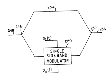
intensity moclulator is shown in FIG. 14. An input
optical wave~lide 246 is connected to an optical
divider 248 which provides 3dB phase coherent power
division. One output of optical divider 248 is
connected through an optical waveguide to a single
sideband optical phase modulator 250. The output of
phase modulator 250 is connected to one input of an
optical combiner 252. The other output of optical
divider 248 is connected to one end of an optical
waveguide section 254. The other end of waveguide
section 254 is connected to the other input of
optical combiner 252. The optical combiner 252 adds
its inputs in a phase coherent manner and provides
an output on an optical waveguide 256. The single
sideband phase modulator 250 is fabricated as shown
in FIG. 10 and described hereinabove. The
., ~
,
c~
90-3-822 -23-
modulation inputs v5(t) and vc(t) are provided
by a transmitter of the type shown in FIG. 11 and
described above. The output of the single sideband
intensity modulator on optical waveguide 256 is an
intensity modulated optical carrier.
A direct detection receiver suitable for
receiving multiple intensity modulated optical
carriers is shown in FIG. 15. The optical signal
received on an optical fiber 260 is connected
through a tunable optical filter 262 to a
photodetector 264. The detected signal is connected
to a an electrical receiver 266. The optical
receiver shown in FIG. 15 is similar to the receiver
shown in FIG. 13 and described above except that the
optical discriminator of FIG. 13 is omitted. The
tunable optical filter 262 is used to select one of
the optical carriers transmitted on optical fiber
260. The intensity modulated optical carrier
selected by filter 262 is detected, and the detected
signal is provided to receiver 266.
For some applications, it may not be necessary
to cancel second-order intermodulation products. In
this case, a single sideband optical phase modulator
similar to the intermod-cancelling optical phase
modulator shown and described above can be used. A
schematic diagram of an intermod-cancelling optical
modulator modified for use as a single sideband
optical modulator is shown in FIG~ 16. The optical
modulator shown in FIG. 16 corresponds to the
optical modulator of FIG. 5, except that the signal
conditioner 102 is omitted, and different modulation
signals are applied to the electrodes. A modulation
voltage vs(t) as given by equation (6) is applied
to electrode 96, and a modulation voltage vc(t) as
given by equation (7) is applied to electrode 100.
Alternatively, the traveling wave
.
:
: . .
90-3-822 -24-
intermod-cancelling optical modulator of FIG. 5A can
be modified and utilized in the same manner. The
output of the single sideband optical modulator
shown in FIG. 16 is given by:
( ) o{coS(~Ot) cos (~S) + sin(~Ot) cos (~ )
+ ~ J~i C09 (Wot + (I)it + ~Si) + 0(~3 )} (14)
where ~5(t) = ~ vs(t)/v~, and
~C(t) = 1~ vc(t)/v~
The first two terms of equation (14) represent
second-order (and other even order) intermodulation .
products. The third term of equation (14) is the
desired upper sideband. Thus, a single sideband
optical modulator with second-order IMP's present in
the output is shown in FIG. 16. This configuration
is useful in situations where second-order IMP's are
relatively small.
While there have been shown and described what
are at present considered the preferred embodiments :-
of the present invention, it will be obvious to
those skilled in the art that various changes and
modifications may be made therein without departing
from the scope of the invention as defined by the
appended claims.
.
:
- .. . .
- ~ ..
, :