Note: Descriptions are shown in the official language in which they were submitted.
I~ f~ S,.n !'~ '~ /~
~~'JJ~) ?;1 .~-,7 :1, .~
ELECTRICAL INTERCONNECT CONTACT SYSTEM
Technical rield
The present invention deals broadly with the field of
electrical interconnect systems. More narrowly, 'however, the
invention is related to technology, for example, for
interconnecting the leads of an integrated circuit device with
corresponding terminals on a printed circuit board interfacing
with a tester intended to effect test analysis of the
integrated circuit device. The preferred embodiment of the
invention is directed to contacts and means for mounting the
contacts for effecting such interconnection.
Laakc~round of the Invention
A plethora of applications exist for effecting electrical
contact between two conductors. One significant application is
effecting interconnection between the leads of an integrated
circuit device and conductive pads or terminals on a printed
circuit board which serves to effect an interfacing between the
integrated circuit device and a tester apparatus. Such
apparatus serve to evaluate performance of. integrated circuit
devices.
Numerpus considerations bear upon the structure employed to
interconnect the IC and the printed circuit board. These
factors bath include electrical and mechanical considerations.
One prior art structure which seeks to accomplish the purpose '
of the present invention 3s known as the Yamaichi contact.
This type of contact~includes an inverted L-shaped support
having a cantilevered contacting portion mounted at the distal
end of the generally~horizontal leg of the inverted, L-shaped
support, and extending generally parallel to that leg. The
distal end of the contacting portion is upwardly turned so that
a point thereof is engageable by a lead of an integrated
circuit device to be contacted. The support, in turn, is
engaged in some manner with or through a pad or terminal
portion of a printed circuit board.
' : . ' . o
.
-2-
One of the mechanical considerations to be taken into
account in designing an interconnect system is that a wiping
action should be accomplished between the contact itself and
the lead of the IC by which the contact is engaged. The wiping
action functions to effect maximization of effee~ive contact in
view of oxide build-up which can occur. In effect, the wiping
action enables a good interlace to be accomplished between the
contact and the lead of the IC.
Tn view of the fact that the cantilevered portion of the
Yamaichi contact has some measure of flexibility, a wiping
action can be accomplished. ~nothar mechanical consideration
that must be taken into account, however, is the desire to
deter bending of a lead on the IC. The Yamaichi contact does
not fully accomplish this goal.
Finally with respect to mechanical considerations, it is
desirable that wiping action~can be accomplished at the
interface between the second end pf the contact and the printed
circuit board. In view of the.construetion of the Yamaichi
contact, it is precluded from allowing such wiping action at
the lower end of the contact.
Further, the Yamichi device does not sufficiently consider
the electrical dictates for an interconnecting contact system.
An interconnecting contact should be a high speed, short path
device. Derivatively, such a contact should have a low
inductance without having a controlled impedance requirement.'
Because of the construction of the Yamaiehi contact. it does
not adequately satisfy these requirements.
United States Patent No. 4,445,735 which issued on May l,
1984 illustrates another type of electrical connection device.
The device of that patent serves to establish an'electrical
connection between contacts of a circuit network on a substrate
and contact pads of a conductor network on a printed oircuit
board. This device is an improvement over the Yamaichi contact
in that it is higher in speed and lower in inductance than the
Yamaichi devic~. It has elastomeric means fox mounting one or
more contacts in a housing. The elastomeric biasing and
mounting enables wiping action to be effected at both upper and
lower ends of the contact. That is, both the end which engages
_3_
an IC lead and the end which engages a printed circuit board
contact pad can be wiped across the surfaces intended to be
contacted.
The device o~ the '735 patent, however, retsina some
limitations, While some wiping action is afforded at both
upper and lower ends of the contact, the amount of such wiping
action is relative limited because of the elastomeric elements
being used generally for effecting biasing rather than free
floating suspension of the contacts. As a result of the
mounting means incorporated in the '735 patent, there will be a
primary tendency for some retraction of the contact point in a
generally vertical direction, but there will be only a small
component of lateral movement to effect wiping. Additionally,
because of the lack of any significant free floating effect,
lead bending on an integrated circuit being tested can occur.
It is to these dictates and shortcomings of the prior art
that the present invention is directed. It is an improved
electrical interconnecting system which addresses the dictates
of the prior art and resolves prablems thereof.
Summarv of the Invention
The present invention is an assembly which functions to
electrically interconnect a lead of an integrated circuit
device to a terminal, for example, of a printed circuit board,,
spaced at a distance from the corresponding lead of the
integrated circuit. The assembly includes a housing which is
interposed between the lead of the integrated circuit and the
corresponding spaced terminal. The housing is provided with at
least one slot, extending therethrough from a first surface to
an oppositely facing second surface. The one or more slots
extend substantially parallel to an axis along which
corresponding integrated circuit lead and spaced terminal are
aligned. The first surface of the housing has, formed thexein,
a trough proximate the location of the integrated circuit lead,
and the second surface of the housing has, formed therein, a
similar trough, the trough in the second surface being disposed
proximate the spaced terminal corresponding ~to an integrated
circuit lead. A rigid first element is received in the trough
formed in the first surface and extends across any slots in
which one or more contacts are received. An elastomeric second
element is received in the trough formed in the second surface
of the housing and extends across the one or more slots in
which contacts axe received. The elastomeric second element is
provided with a measure of compressibility and tensile
extendibility. A generally planar contact is received within
one or more of the slots, each contact having a protrusion
extending outward from the first surface of the housing to be
engaged by an integrated circuit lead. Each contact also lice a
nub normally extending outward from the housing toward the
second surface of the housing to engage a corresponding spaced
terminal. I'urther, each contact has a hook portion proximate
the nub o~ the contact, the hook portion encircling the
elastomeric second element to hold the contact to the
elastomeric second element. Each contact has formed therein an
elongated channel to receive the rigid first element therein
for relative movement of that element along the channel.
Relative movement results as the protrusion of the contact is
engaged by, and urged inwardly into the housing by, an
integrated circuit lead. The assembly functions, as a result
of the rigid first element moving relatively along the channel
formed in the contact, wherein the protrusion of the contact
moves across the integrated circuit lead by which it has been
z
engaged, and the nub of the contact moves across the
corresponding spaced terminal of the printed circuit board.
In one embodiment of the invention wherein the trough
formed in the first surface of the housing is substantially
symmetrical with respect to a plane normal to the first
surface, an axis of elongation of the channel formed in each of
the contacts is at an angle relative to such a plane.
Typically in this embodiment, the trough formed in the second
surface of the housing is laterally offset from that formed in
the first surface. As a particular lead of an~integrated
circuit device engages the protrusion of a corresponding
~5-
contact and exerts downward pressure upon the protrusion, the
channel in the contact will move relatively to the rigid first
element received therein, and the contact will, effectively, be
made to rotate to some extent as a result of the rigid first
element moving, relative to the contact. more deeply into the
channel formed in the contact. The downward.force exerted by
the lead of the integrated circuit upon the contact will have
components along both X and Y axes, and these components will
effect the apparent rotation of the contact. 1~s a result, the
protrusion will move laterally to some degree across the
surface of the integrated circuit lead by which it is engaged,
and the nub of the contact will move laterally across the
integrated circuit board terminal with which it is in contact.
In another embodiment of the invention, a plurality of
slots, each receiving a contact, are provided. Typically, a
multiplicity of contacts are emplayed. one for each integrated
circuit lead. In such an embodiment, the printed circuit board
is provided with a plurality of terminals, each being in
engagement with one of the ganged contacts.
In such a multiple contact embodiment, an additional
elastomeric second element can be provided. The additional
elastomeric second element being disposed in a second trough
formed in the second surface of the housing and being
symmetrical, with respect to the initial elastomeric second i
element, relative to the rigid first element. Contacts in '
immediately adjacent slots can be staggered (that is,
alternately hooked to the initial elastomeric second element
and the additional elastomeric second element). By providing
such a structure twice the contacting density per unit length
can be provided.
In this embodiment, a trough need not be provided to
receive the rigid element. Since there are at least two
oppositely-acting, cooperating contacts, the rigid element will
be maintained within the channels o~ the contacts. Since the
channels are angled in opposite directions, they will cot as
jaws to hold the rigid element in place.
~~~<~~:~.~'~
Another embodiment employs an elastomeric elongated element
in the trough formed in the first surface of the housing rather
khan a rigid element. This embodiment would employ a hook
member proximate the protrusion of the contact at the upper end
thereof rather than an elongated channel as in the
first-described embodiment. The contact would, therefore,
latch onto the upper elastomeric element as it does onto the
lower elastomeric element. In this embodiment, the contact is
more free-floating than in the previously described
embodiment. '
The present invention is thus an electrical contact
interconnecting system improved over systems of the prior art.
More specific features and advantages obtained in view of those
features will become apparent with reference to the DETAILED
DESCRIPTION OF THE INVENTION, appended claims, and accompanying
drawing figures.
flrief Description of the Drawings
A
Figure 1 is an enlarged fragmentary perspective view of one
embodiment of the present invention illustrating plural
contacts;
Figure 2 is a perspective view of an individual contact o~
the embodiment of Figure 1:
Figure 3 is a fragmentary functional diagram showing the
embodiment of the invention of Figure 1 sectioned vertically "
and at rest;
Figure ~4 is a view similar to Figure 3 showing the contact
engaged by an integrated circuit device lead;
Figure 5 is a view similar to Figure 3 showing the contact
being manipulated in order to effect connection or
disconnection to the rigid and elastomerie members;
Figure 6 is a fragmentary side elevational view of anothex
embodiment of the invention with some parts cut awayt
Figure 7 is an enlarged view similar to Figure 6 showing
articulation of a contact in dashed lines;
Figure 8 is a fragmentary side elevational view with some
parts cut away showing an embodiment of the invention in signal
mode contact configuration;
Figure 9 is a view similar to Figure 8 showing the
embodiment in a decoupling mode contact configuration:
Figure 10 is a fragmentary side elevational view with some
parts cut away showing another embodiment of the invention; and
Figure 11 is a fragmentary top view of the embodiment of
Figure 10.
Detailed Description of the Invention'
Referring now to the drawings wherein like reference
numerals denote like elements throughout the several views,
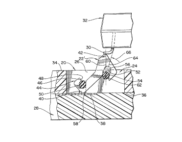
Figure 1 illustrates a housing 20 suspending a plurality of
contacts 22 in accordance with the present invention. The
housing 20 shown in Figure 1 is representative of a housing
usable in virtually all embodiments of the invention, although,
in some embodiments, some variations, generally unrelated to
contact mounting, could Toe incorporated.
Some portions of the housing 20 are broken away in Figure
1, but one viewing the figure can count at least seven slots 2~.
formed through the housing 20. The rightmost of the slots 24
is sectioned so that only one side wall 26 of the slot 2A is
able to be seen.
L4hile seven slots 24 are illustrated, only four contacts
22are shown as being disposed in slots 24. It will be
understood, however, that, typically, a contact 22 would be
suspended within the housing 20 in each slot 29 provided,
although this would not be essential. Additionally, it will be
understood that any number of slots 24 could be provided, and
the slats 29 could be organized in multiple arrays. For
example, tour arrays of slots 2~ defining a quadrilateral form
could be employed. Such a configuration would be employed when
the housing 20 in accordance with the present invention is
intended to interconnect a printed circuit board 28,
interfacing with a tester mechanism (not shown), to the leads
30 of, for example, a leadless chip carrier integrated circuit
device 32. Figure 1, therefore, is merely illustrative o~ a
rudimentary 7iouaing 20 in accordance with the invention.
?~~~:~:~'~
_Q_
As seen in Figure l, the rightmost slot 24 is shown as
extending fully through the vertical dimension of the housing
20 from a first, upwardly Facing surface 34 of the housing 20,
to a second downwardly~facing surface 36 of the housing 20.
The same is true of each slot 24..
The second surface 36 of the housing 20 is shown as being
in engagement with a printed circuit board 28 having at least
one pad or terminal 38 traced'thexeon. Such a pad 38 is
intended to be engaged by a nub 40 at the lower end of the
contact 22 as will be discussed hereinafter. In view of the
fact that the nub 40 is biased to extend outwardly at least to
the second surface 36 of the housing 20, when the printed
circuit board 28 is held in position in engagement with the
second surface 36 of the housing 20, the nub 40 of the contact
will, in fast, engage the pad 38 if the pad 38 is properly
positioned spatially.
Figures 6 and 7, to which further reference will be made in
describing the embodiment thereof, shave a contact 22' suspended
in a housing 20 in a manner discussed hereinafter. fihe contact
22' has a small measure of elongation and has a protrusion 42
at its upper end, the protrusion 42 functioning to be engaged
by a lead 30 from an integrated circuit device 32 intended to
be interconnected to the printed circuit board 28. As seen in
.x
Figures 6 and 7, when the conta~t 22' is suspended by the
housing 20, the protrusion 42 extends upwardly beyond the fiist
surface 34 of the housing 20.
As previously discussed. the contact 22° has, at its lower
end, a nub 40. The nub 40 is, of course, intended to engage
the terminal or pad 3B on the printed circuit board 28 which
corresponds to a particular integrated circuit lead 30 engaged
by the protrusion 42 of the respective contact 22'.
Proximate the~nub 40 is a hook portion 44 of the contact
22'. The hook portion 44 defines a generally circular aperture
46 which is pinched at the entry thereto, as at 48, so that,
when the hook portion 44 is urged over an elastomeric element
50 as defined 'hereinafter, the contact 22' will be maintained
in a position suspended with respect to the elastomeric element
S0.
_g_
The contact 22', proximate its upper protrusion end, is
provided with an elongated channel 52. This channel 52 is
intended to receive a rigid element 54 as defined hereinafter.
Referring now again to Figure 1 which illustrates a
representative housing 20, the first surface 3~ of the housing
20 is provided with a trough 56, that trough 56 extending
across, and generally transverse to, the plurality of slots
24. In a like manner, the second surface 36 of t'he housing 20
also has a trough 58 formed therein. This trough 58 also
extends across the various slots 2~ and is illustrated as being
generally transverse to the direction bf orientation of the
slots 24. Each trough 56, 58 is shown as being generally
symmetrical with respect to an imaginary plans 60 that would be
perpendicular to the respective surface in which the trough 56,
s~
58 is formed. It will also be noted that the troughs 56, 58
are laterz~lly offset from one another fox a purpose that will
become apparent in view of subsequent discussion.
The trough 56 formed in the first surface 3A is intended t~o
accept the rigid element 54 in the case of the embodiment of
Figures 6 and 7. The element 54 is shown as extending, fully
across the array of slots 24 across which the trough 56 in
which the element 5~1 is received extends.
In that embodiment, the trough 58 formed in the second
surface 36 of the housing 20 is intended to accept a
compressible, tensiley extendable, elastomeric element 50
therein. In the case of the rigid element 54 received in the
trough 56 Formed in the first surface 3A of the housing 20, the
elastomeric element 50 received in the trough 58 formed in the
second surface 36 of the housing 20 is intended to extend fully
across the array of slots 24 across which the trough 58 in
which the elastomeric element 50 is received extends.
Mounting, or suspension, of individual contacts 22' in the
embodiment of Figures 6 and 7 can be affected in any
appropriate manner. One simple manual way of effecting
suspension would be to insert the contact 22' downwardly
through the slot 24 within which it is to be received by urging
the nub ~l0 end between the rigid element 54 and the elastomeric
-10-
element 50, those two members having been received within their
respective troughs 56, 58. Once the hook portion 44 has been
inserted to a point at which it has achieved a location below
the elastomeric element 50, the hook portion 44 can be moved
laterally to "catch" the elastomeric element 50 tharewithin.
After such "catching" has occurred, the contact 22° would be '
withdrawn upwardly to a point at which the entrance to the
elongated channel 52 in the contact 22' is above the upper edgy
of the rigid element 54. The protrusion end of the contact 22'
can then be moved in a direction to the right, as viewed in
Figures 6 and 7, until the entrance 62 to the channel 52 is
above the rigid element 54. xt will be understood that, as the
contact 22' is withdrawn upwardly, the elastomeric element 50
will come under tension when the contact 22' is in a
disposition wherein the entrance 62 to the channel 52 is above
the rigid element 54. When the contact 22' is in such a
disposition, the contact 22' can be eased downwardly so that
the rigid element 54 enters the channel 52. The tension on the
elastomeric element 50 will, thereby, bs released, and the
contact 22' will be in its "rest" position. This procedure can
be performed for multiply contacts 22' when a gang or array of
contacts 22' is employed.
The "rest" position of a contact 22' is represented in
solid line in Figure 7. The center-line axis 64 of the channel
52 is angled slightly to the right of a plane of symmetry 60.of
the trough 56 within which the rigid clement 54 is received.
That plane of symmetry 60 is generally normal to the first
surface 34 of the housing 20 and is represented by a dashed
line. The center-line axis 64 of the channel 52 formed in the
contact 22' is represented by an additional Tine 64 in Figure 7
at a slight angle with respect to the line representing the
plane of symmetry 60 of the trough 56: An angle representation
66 indicates the angle at which the channel 52 is tilted ~rom
the plane of symmetry 60 of the trough 56. This angles 66 can
be, in the "rest" position of the contact 22' , quite small and
probably, it is anticipated. of a magnitude of between about 3'
and. 30' .
~11-
Figure 7 also illustrates the movement of a contact 22' as
the grotrusion 42 of the contact 22' is engaged by a lead~30 of
an integrated circuit device 32, As the integrated circuit .
device 32 is brought into engagement with the protrusion
engagement point and downward pressure continues, the rigid
element 54 rides upwardly, relative to the elongated channel 52
in the contact 22', and the angle of offset 66 of the axis 64
of the channel 52 becomes more exaggerated. As this occurs,
the engagement point of the protrusion 42 is moved downwardly
and to the right. The rightward movement of the engagement '
point of the protrusion 42 will permit relative movement of the
engagement goint across the surface of the integrated circuit
load 30. This wiping action will provide for a better
electrical flow path between the integrated circuit lead 30 and
the protrusion 42 of the contact 22'.
One of the reasons why the apparent rotation of the contact
22' will occur is that the nub end of the contact 22' will be
precluded from downward movement by the terminal or pad 38 of
the printed circuit board 28. As previously discussed, in the
embodiment illustrated in Figures 6 and 7, the printed circuit
board 28 is substantially in engagement with the second surface
36 of the housing 22'. The vertical location of the deegest
part of the trough 58 formed in the second surface 36 0~ the
housing 20 relative to the dimensions of the lower portion of
the contact 22' will provide for biasing of the nub 40 of the'.
contact 22' into engagement with the printed circuit board pad
38. As the integrated circuit 32 urges the protrusion 42 of
the contact 22' dotunwardly, therefore, the nub 40 will be
driven in a direction to the left as viewed in Figure 7.
Wiping action will, thereby, occur, and the electrical flow
path between the nub 40 of the contact 22' and the printed
circuit board terminal 38 will be optimized.
Figures 8 and 9 show contacts and contact suspension means
as illustrated in Figures 6 and 7 to illustrate signal and
decoupling modes of the housing 20. Figure 8 illustrates the
invention embodiment in a signal mode configuration. This view
shows the contacts 22' configured to interface signal terminals
or lands 68 on the printed circuit board 28.
-lz-
Figure 9 illustrates a decoupling mode. In the decoupling
mode, the integrated circuit device 32 has multiple ground and,
sometimes, multiple power leads which need to be connected by a
capacitor 70 to'allow current response when outputs of the
integrated circuit devise 32 are switched. In the prior art,
the customer is assisted in meeting needs for specific device
configurations of ground and power locations. These locations
are virtually always located near the center of tire sides,
since the internal lead inductance is the smallest. The
housing 20 is designed to permit center contacts to be mirrored
to allow ground and power leads to directly contact one of
multiple decoupling planes 72. Rach decoupling plane 72 used
is designated as either a ground or power plane so that, when a
chip capacitor 70 is soldered across these planes 72, a
deccupling circuit will be formed.
Doth the signal terminals or lands 68 and the decoupling
planes 72 are connected to external customer circuits. The
contacts 22' are shown as mirrored to allow for direct
integrated circuit electrical connection to the decoupling
planes 72. The decoupling planes 72 are decoupled by a chip
capacitor 70.
The contacts 22 illustrated in Figures 1-5 are different
than those illustrated in Figures 6-7. Figure 2 illustrates an
alternative form contact 22 isolated from a slot 24 within the
housing 20. The primary difference between this contact 22 and
that previously described is that the contact 22 does not have
an elongated channel 52 proximate the upper protrusion
portion. Rather, the contact 22 of Figures 1-5 is provided
with a hook portion 74 similar to the hook portion 44 proximate
the nub 40 of the contact embodiment previously described.
When the contact 22 illustrated in Figures 1-5 is employed,
a different type of element 76 would be seated in the trough S6
formed in the first, or upper, surface 34 of the housing 20.
Rather than providing a rigid element 54, the element 76 which
would be received in the trough 56 in the first surface 34 of
the housing 20 in this embodiment would be elastomeric in
nature and similar to the element 50 in the trough 58 formed in
the second surface 36 of the housing 20. Hoth elements would,
-13-
therefore, have a measure o~ compressibility and tensile
extendability rather than only one element having such
compressibility and tensile extendability, as is the case with
the embodiment of Figures 6 and 7.
With both elements being elastomeric in nature, movement of
both the protrusion 42 and nub 40 of the contact 22 would still
be able to occur along twa mutually-perpendicular axes. That
is, both the protrusion 42 and the nub 40 of the contact 22
could move generally horizontally and vertically in view of the
compressibility of the two elements. The embodiment of Figures
1-5, therefore, would also achieve the desired wiping action.
At the same time, integrated circuit lead damage would be
minimized, since the contact 22 is substantially free-floating
in its suspension within the housfng 20.
It will be understood that the response of the system can
be controlled by varying the durometer rating of the element 76
received within the trough 56 formed within the upper surface
34 of the housing 20. The harder that the element 76 is, the
more resistant it will be to lateral motion of the contact
protrusion 42, and wiping action of protrusion 42 across the
lead 30 of an integrated circuit 32 will be reduced. A typical
durometer range is between 30 and 90,Shore D.
Figure 3 illustrates the contact 22 of the embodiment of
Figures 1-5 in its normal "rest" position. In this position,
both elastomeric elements 50, 76 extend substantially
linearly.
Figure 5 illustrates the manner in which the elastomeric
elements 50, 76 could be manipulated in order to effect
mounting. Figure 5 shows a contact 22 having been inserted
upwardly through the bottom, second surface 36 of the housing
20 so that the protrusion 42 of the contact 22 passes between
the two elastomeric elements 50, 76 and the hook portion 74
proximate the protrusion 42 of the contact 22 is positioned
above the elastomeric element 76 received within the trough 56
formed within the first surface 34 of the housing 20. The
upper hook portion 74 then is brought downwardly to "catch" the
elastomeric element 76 received in the trough 56 formed in the
first surface 34 of the housing 20. .Figure 5 illustrates the
contact 22 with such attachment to the elastomeric element 76
received in the trough 56'formed in the first surface 34 of the
,,
-14-
housing 20 being drawn downwardly to deform that element 76 so
that the lower hook portion 44 can be brought into a
disposition at which it can '°catch" the elastomeric element 50
received in the trough 58 formed in the second surface 36 of
the housing 20. When the lower hook portion 44 is brought into
such a position, the contact 22 can be gradually released to
effect catching of the elastomeric element 50 received in the
trough 58 formed in the second surface 36 of the housing 20.
After his occurs, the contact 22 and the elastomeric elements
50, 76 assume the positions illustrated in Figure 3.
Figure 4 illustrates the response of the assembly when the
lead 30 of an integrated circuit 32 is brought into engagement
with the protrusion 42 of the contact 22. As can be seen, the
elastomeric elemont 76 received in the trough 56 formed in the
first surface 34 of the housing 20 is deformed downwardly as it
undergoes compression and tensile extension.
With the nub 40 of the contact 22 in engagement with the
terminal 38 on the printed circuit board 28, there will be a
deformation of the elaetomeric element 50 received in the
trough 58 formed in the second surface 36 of the housing 20.
Aa seen in Figure 4, this deformation will have an apparent
upward movement.
In the embodiment illustrated in Figures 1-5, the printed
circuit board 28 might, initially, be spaced ~rom the second
surface 36 of the housing 20. As the lead 30 0~ the integrated
circuit device 32 is brought into engagement with the
protrusion 42 0~ the contact 22 to urge the protrusion 42
downwardly, the lower extremity of the contact 22 (that is, the
nub 40) will come into engagement with the terminal 38 of the
printed circuit board 28. As continued downward movement of
the protrusion 42 of the contact 22 occurs, co-related upward
movement of the nub 40 will result. This movement of the
contact 22 will function to accomplish wiping and protection of
the integrated circuit lead 30.
Figures 10 and 11 illustrate an embodiment akin, in some
reepecta, to the embodiment of Figures 6 and 7. In this
embodiment, a rigid element is employed and is received in the
elongated channel 52 of each of a plurality of contacts 22'.
~~r~~~):~~.'~
-15-
In this embodiment, however, contacts 22' in adjacent slots 24
are staggered. That is, while one contact 22' extends to the
left as seen in Figure 10, the next contact 22' extends to the
right.
It will be understood, and it is illustrated in Figures 10
and 11, that an additional elastomeric element 78 is provided,
since hook portions 44 of the various contacts 22' in the array
extend on two sides of the central, rigid element 54. In order
to accommodate the additional elastomeric element 78, a second
trough 80 is formed in the second surface 36 og the housing
20. The trough 80 would be spaced laterally from an intended
location of the rigid element 54 substantially the same
distance that the initial elastomeric element 50 is spaced in
an opposite direction. As a result, the contact array will
appear symmetrical. This arrangement is best seen in Figure
10.
In the embodiment of Figures 10 and 11, a trough need not
be provided in the first surface 34 of the housing 20 to
receive the rigid element 54. Because of the oppositely
coacting contacts, the rigid element 54 can be received in
various elongated channels 52 in the contacts 22', and the
reciprocal cooperation of the contact channels 52 will result
in a jaw effect whereby the rigid element 54 is held in the
channels 52.
Since a trough need not be provided for receipt of the
rigid element, material need not be expended in forming the
housing 20 at the location where the rigid element 54 is
disposed. As seen in Figure 10 then, a generally V-shaped
recess 82 can be formed in the housing 20 with a central wall
84 extending upwardly from the second surface 36 of the housing
20 to separate left and right slots 24 . Material from which
the housing 20 is formed can, theroby, be conserved.
As seen in Figure 11, the slots 2~1, typically, have an
axial dimension greater than that of the respective contacts
22'. Consequently, there can be some play with the contacts
22° not being maintained in continuously defined planes. Since
the contacts 22' are conductive in nature, insulative washers
B6 can be disposed between adjacent contaets~22' along the
-16-
rigid element 54. The axial dimension o~ the washers 86 can be
such that play among the contacts 22' can be minimized.
Figure 10 illustrates an integrated circuit device 32 with
its leads 30 being brought into engagement with the protrusions
42 of the various contacts 22'. Figure 10 illustrates those
leads 30 as being spaced laterally in order to conform to the
positions of the protrusion 42 of the contacts 22'. an fact,
it will be understood that the slots 24 and respective contacts
22' received therein can be constructed in a manner so as to
accommodate integrated circuits 32 structured in any particular
fashion.
Regardless of the embodiment of the invention, the housing
20 is substantially the same, varying only based upon the
intended location of the contacts 22'. The housing 20 can be
fabricated by forming the slots 24 with either laser machining
(typically, for prototyping and sm~l1 production quantities) or
injection molding of the overall housing 20 with slots 24
formed therein (typically, for economic production
quantities). Contacts 22, 22' can be suspended in a manner
previously discussed. As one will perceive, contacts 22, 22'
are individually replaaeable~.
The contacts 22, 22' are~designed to provide very short
electrical paths. Typically, the overall length of a contact
would not exceed.0,14 inches. In contacts in accordance with
the present invention, such a length translates into a 2.0
nanohenries inductance between surfaces. As a result, very
high digital signals (typically greater than 100 megahertz) can
be transmitted without any significant loss of fidelity. Since
the areas of the contacts 22, 22' which actually engage
integrated circuit device leads 30 and printed circuit board
terminals 38 is minimal, the amount of cross-talk between
signal lines will also be minimal. This will provide for
higher isolation of transmitted analog signals.
Numerous characteristics and advantages of the invention
have been set forth in the foregoing description. It will be
understood, of course, that this disclosure is, in many
respects, only illustrative. Changes can be made in details,
particularly in matters of shape, size, and arrangement of
'. w '
a
-17-
parts without exceeding the scope of the invent3.on. The
invention's scope is defined in the language in which the
appended claims are expressed. ,
r