Note: Descriptions are shown in the official language in which they were submitted.
2 ~
~AVBG~DE ~AN~T~ON ~OR ~L~ P~B ~N~NA
BA~RGRO~ND OF T~B INVE~IO~
The present invention is another o~ a series of
improvements s~emming from an initial development by the
assignee of ~his application, in the area o~ flat an-
tennae. That initial development, disclosed and claimed
in U.S.PO 4,761,654, relates to a ~lat plate or printed
circuit antenna in which all of the elements, including
the ground plane, feedline, ~eeding patches, and radia-
ting patches, are capacitively coupled to each other.
The inventive structure enables either linear or circu
lar polarization. A continuation-in-part of that appli-
cation, application No~ 06/930,187, now ~.S.P.
5,005,019, discloses and claims slot~shaped elements.
The disclosures of these patents are hereby incorporated
herein by reference.
Previously, in such flat plate antennae, it has
been known to provide input power to the array at a
sinyle feedpoint, and then to use a printed line, such
as stripline, to carry power through a power divider
network (PDN) to the various elements of the arrayO
However, for large arrays, such as those which are
perhaps one meter wide, using a printed distribution
line results in unacceptably high losses. It would be
desirable to minimize these losses.
Another copending, co~monly assigned application,
No. 07/210,433, disclose~ two improvements, including
the incorporation of a low noise block (LNB) down con-
verter into the power divider structure, at a sacrifice
of array elements. Another improvement disclosed there-
in is the use of coplanar waveguide technology to pro~
vide a power connection to the feedpoint of ~he array.
The remainder of the feeding to the elements o~ the
array is done in stripline, or another type of techno~
logy such as microstrip, finline, or ~lotline. ~he
2~3~
disclosur~ of ~hat c:opending apl?lication also is
incorporated herein by reference.
The limi~ed use of the waveguida structure, and the
resulting extensive use of etched power distribution
lines in the antenna results in undesirably high 105S.
811~Y OP'_T~ INV13~1TIVN
In view of the foregoing, it is a primary object of
the invention to provide a feed s~ructure for a flat
plate antenna which results in lower loss and thus in
improved performance.
To achieve the foregoing and other objects and ad-
vantages, the invention disclosed herein provides a Plat
plate antenna with a feed structure partially implemen
ted in waveguide, rather than using cnly a printed
distribution line. The array is ~ed at a single point,
using a coaxial connection through the ground plane.
Waveguide structure is attached to the back of the
ground plane, using the ground plane itself as a top
wall for the waveguide.
For arrays of relatively small size, the waveguide
structure is incorporated to provide feeding to a limit-
ed number of points in the array, whereupon a printed
distribution line is used. However, for larger arrays,
where losses hecome greater because of the greatly
increased amount of printed distribution line which
would be necessary, a more extensive waveguide structure
is provided, with a plurality of transition points in
different quadrants of the array.
Because the invention is directed solely to the
power feed structure for a flat plate antenna, implemen-
tation of the invention need not be restricted to a
particular type of radiating element. Rather, radiating
elements such as those disclosed in U.S.P. 4~761,654 and
5,005,019 may be used. Further, the invention is
applicable not only to single-polarization
. .
.
2 ~
implementations such as those just mentioned, but also
is applicable to a dual~polarization structure, such as
that disclosed in U.S~R. 07/165,332, now UOS.P.
4,929,959, and U.S.P. 07/192,100, now U.S.P. 4,926,189.
This last U.S. patent also discloses another type of
radiating element, which also may be used with the
present invention. The disclosures of these patents
also are incorporated herein by re~erence.
Further, implementation o~ the invention would not
be hindered if structure such as that shown in copandiny
application No. 07/210,433 were to be used. Thus, it
can be seen that the invention has wide applicability to
a number o~ structures and technologi2s in the ~lat
plate antenna area.
B~ DE8C~IPTIO~ O~ T~E DR~IN~,8
The ~oregoing and other features and advantages of
the invention will be more readily apparent from the
ollowing description taken in conjunction with the
accompanying drawings, in which:
Figure 1 shows a plan view of feed structure
incorporating the invention;
Figures 2A and 2B show transverse cross-sectional
views of the structure of Figure 1 in a flat antenna/
and Figure 2C shows an alternative implementation o~ the
transition structure of Figure l;
Figure 3 shows an implementation o~ the structure
of Figure 1 in a multi-quadrant implementation, ~rom the
underside o~ tha antenna;
Figure 4 shows a cross-sectional view o~ a dual~
polarization antenna showing the inventive waveguide
~eed structure; and
Figures 5-9 show graphs of results attained with
the inventive structure, in a single-quadrant and multi-
quadrant implementation.
.
20~3~4
D~TAI~E~ DB8C~IPTIQN 0~ ~B P~F~RBD ~MBOD~BN~
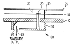
As seen in Figure 1, power divider network layar lS
of a flat plate antenna is fed Yia a central feeding
location 20 which, in the disclosed embodiment, is a
waveguide input to a waveguide-~-plane bend. The E-
plane bend structure is shown in greater detail in
Figures 2B and 2c, and will be discussed below. In the
present emhodiment, a coaxial probe transition is
provided. The connection 20 feeds the layer 15 at a
~ingle ~eedpoint, through a hole drilled in the ground
plane 10. The single feedpoint implementation is
essentially the same as that described in copending
application No. 07/210,433. The coaxial connection 20
feeds a quarter~wave transition portion 40A, to
printed distribution n~twork 40~ on power divider
network layer 15.
The probe 20 itself is optimized in length, and
tuned to a desired frequency. At the fs~dpoint there is
a quarter wave transformation 40A to stripline 40B.
Mode suppression walls 30, parallel to each other and
provided on opposite ~ides of the coaxial feed 20, are
providad ~or impedance matching purposes, and to
facilitate the transition ~rom waveguida to stripline~
One wall o~ tha waveguide 100 ~Figure~ 2A, 2B, and
3) is Pormed by the ground plane lo itself~ The other
three walls of the waveguide 100 may be either a cast
metal piece or metallized pl~stic, attached to the back
of the ground plane lo. The waveguide it~elf is a well~
known type of rectanqulax waveguide, so that the inner
dimension is rectangular.
In Figure 2A, a wedge or metal plate 120 is
provided at an opposite ~nd of the waveguide from the
probe 20~ at a 45 angle to the direction of propagatisn
of the waveguide output, and opposite a waveguide
.
' ' ' ' ~:
,
opening 125. The purpos~ o~ the wedge is to bend, at a
90 angla, the propagatiarl path of the waveguide output.
As ment.ioned above, the lenyth of the probe is
optimized 50 as to be tunable to the desired frequency.
Also, the match into the waveguide can be tuned by pro-
viding the end wall 110 of the waveguide 100 an approp-
riate di~tance d from the probe. Thus, the probe
~unction is optimized by tuning in this fashion, and
also by providing the mode suppression walls 30 in a
vertical plane at the initial connection poink and
running along the power divider network of the array, to
suppre~s the unwanted parallel plate mode. Without the
mode suppression walls 30, energy can propagate out the
sides, and provide inefficient coupling into the power
divider. These vertical walls run the fuLl height
between the stripline and the ground plane, pxoviding a
type of suspended substrate at the initial kransition
point, and thus effectively provide four walls that com-
pletely surround the connection. Preferably, the mode
suppression walls 30 are a distance on the order of ~/4
from the coaxial probe 20, and axe on the order of ~/2
long, where ~ is the wavelength of the radiation of
interast.
The quartsr wave transformation me~tioned above
matches the waveguide into the power divider nPtwork~
For example, in the presently known impl~mentation, the
coaxial feed is approximately 50 ohms, and is matched
into a 70 ohm impedance.
An alternative feed structure, u~ing a direct
waveguide/stripline transition, is shown in Figure 2C.
In this implementation, a second wedge or metal plate
130 is pravided in lieu of the probe 20. The waveguide
extends through the ground plane 10, the power divider
network layer 15, and the radiating elsment layer 25, as
hown, directly to the stripline. Because of the two
2~93~
wedges 120, 130, there are two E plane bends in the
propagation path, as sho~n by the arrow. Tuning of this
structure is effected by adjusting the extent of wave-
guide penetration through the ground plane, and also by
adjusting the distance that the stripline extends into
the waveguide.
For a large structure, as shown in Yigure 3~ the
array may be divided into four quadrants, with a feed-
point 20A-20D in the center of each quadrant, and the
central feeding location 2Q as shown in Figure 1. At
each feedpoint 20A-20D, mode suppression walls 30 and
quarterwave transition~ 40A to stripline 40B ~re
provided. A waveguide network 100 is provided on the
back of the array, beneath the ground plane 10, the
ground plane 10 itself acting as a top wall for the
waveguide, as mentioned earlier. Because of the low
loss of the waveguide structure, the overall efficiency
of the array is substantially better than that of an
array usiny only a printed power distribution line.
Figures 8 and 9, for example, show comparative results
between an antenna using the inventive feeding technique
(Figure 8~ and an antenna using a conventional feeding
technique (Figure 9)~ The inventive antenna i5 1 . 5 to
2.0 dB better across the bandwidth of interest.
Naturally, there is some trade-o~f between the cost
o implementing waveguide and the gain in e~ficiency.
This is why for a larger array, which would require a
correspondingly larger power distribution network and
thus correspondingly larger losses, it is ~esirable to
have waveguide implemented more extensively on the back
of the ground plane. Larger arrays es~entially are
divided into quadrants, with the waveguide being
provided as a feed to each of the quadrants.
Losses in the power distribution network degrade
the signal in two different ways. First, the gain or
: `
'
.
3 ~ ~
~he pow~r of the s.ignal is decrea5ed, thus lowering the
signal to noise (S/N) ratioO In addition to attenuating
the signal level, thz loss adds random noise to the
signal, thus increa~ing the denominator of the SJN
ratio.
The implications may be c~nsidered as ~ollows. For
example, for these types of antennae, th~ distance from
the central ~eeding location to the outer elements is
approxi~ately equal to the length of one side of the
array. Thus, for an antenna that is one foot square,
the distance from the output to a particular element i5
approximately one foot. For dis~ances o~ this length,
the lo~s is not appreciable, bu~ ~or di~tances as large
as a meter (i.e., for arrays khat are one meter square),
the loss does ~ecome signi~icant, there~y making it
advisable to provide the waveguide transition.
By substituting the higher-loss printed line with
the waveguide, especially ~or larger arrays, total loss
being a function o~ the total length from the output to
the element, both of the aspects of degr~dation of the
S/N ratio discussed above ara compensated.
The single-fePd structure for a smaller array
yields a single feed confi~urationl as seen ~or example
in Figure 1, and Figures 2A and 2B. For a multi-
quadrant structure such as shown in Figure 3, essen-
tially there are three TS. At tha ends of the last two
Ts, thère axe feeds and trànsitions frum waveguide to
stripline~
Figures 2A and 2B show a cross-sectional view of
the flat plate antenna for a single-polarization
structure, including a radiating element layer 25. It
should be noted, as discussed in the above~mentioned
patents, that the radiating elements in lay~r 25 are
impedance matched with the feedlines in power divider
2~3~
network layer 15. Those feedlines may have any o~ the
shapes disclosed in the above-mention2d pa~entsO
The preferred height of the mode suppression walls
~o is equal to the full height between the ground plane
10 and the radiating element layer 25, extending through
the power divider network layer 15.
A dual-polarization structure also is possible, as
shown in Figure 4. Such a structure includes an addi-
tional power divider network 35 overlying the radiating
element layer 25, and an additional radiating element
layer 45 overlying the top power divider networX 35.
The radiating element layer 25 acts as a ground plane
for the overlaid structure. The elements in layer 25
are disposed orthogonally with respect to those in layer
45. Thera are two waveguide structures 100 and 100l,
also disposed orthogonally with respect to each other,
and two coax probes 20, 20'. Mode suppression walls 30
extend between qround plane 10 and radiating element
layer 25, and mode suppression walls 30' extend between
the layer 25 and the upper radiating element layer 45.
Comparative results showing the perfo~mance o~ the
array using waveguide relative to results attained using
conventional stripline are shown in Figures 5-9.
Figures 5 and 6 show return loss and gain results ~or a
single quadrant (256~element) implementation. As can be
seen from tha~e Figure~, single-probe feeding provides
very good input return loss with a corresponding high
aperture e~iciency (~5-90%) for small apertures (on the
order of 10~ to 15~).
Waveguide integration is amployed ~o maintain the
single-probe effi~iency for larger apertures ~20~ to
30~). Figures 7 and 8 show results for a multi-quadrant
(1024-element) implementation. As can b~ seen, the
input return lo~s is of the same order as for the
single-probe implementation, and the swept gain is very
'
.
`
~93~
near th~ ideal 6 dB incrPase, corresponding to an
aperkure efficiency o~ 80-85%.
The results in Figures 7 and 8 may be contrasted
with ~hose o~ Figure g, for a conventional 1024-element
structure that employs an all-stripline pcwer distribu-
tion network. Figure 9 shows swept gain 1.5 to 2.0 dB
lower than that o~ the inventive antenna, corresponding
to only a 50~60% aperture ef~iciency.
As mentioned above, the power feed structure of the
lo invention is applicable to flat plate antennas using a
variety of types of radiating elements, such as those
shown in the just-mentioned u.S. patents and copending
applications. Thus, the inventive ~eed technique finds
application not only in single~ and dual-polari~ation
implementations, but also to both lineax and circular
polarization implementations are contemplated. Still
urther, while striplin~ is the presently-pre~erred
implementation of the power distribution network for
receiving the transition ~rom wave~uide, other struc-
tures, including finline, slotline, and microstrip arewithin the contemplation of the invention.
~ hile the invention has been described in detail
above with referencQ to a preferred embodiment, various
modifications within the scope and spirit of the inven-
tion will be apparent to people of working skill in thistechnological field. Thus, the invention should be
considered as limited only by the scope of the appended
claims.
.. . . .