Note: Descriptions are shown in the official language in which they were submitted.
2053396
COMPACT DBVICB FOR ~KlNG A HBADBR BRROR
IN A~ KuNOUS TRANSFBR MODB CBLLS
Backqround of the Invent lon:
Thls lnvention relates to a devlce for monltorlng
ATM ~asynchronous transfer mode) cells used ln an STM
(synchronous transfer mode) slgnal and to a header error check
(HEC) device for checking a header error in the ATM cells.
The ATM cells are transmitted in a synchronous
transfer mode as the STM signal. The synchronous transfer
mode is used on various levels. When transmitted ln the
synchronous transfer mode of a level M, where M represents a
prescrlbed natural number, the STM signal is called an STM-M
signal. An STM-l slgnal ls transmltted at a blt rate of
155.52 Mblts/s and comprlses 2,016 telephone channels. An
STM-4 signal is transmitted at a higher blt rate of 622.08
Mblts/s and comprlses 8,064 telephone channels. An STM-16
slgnal ls transmitted at a still higher bit rate of 2,488.32
Mbits/s and comprlses 32,256 telephone channels.
- 64768-260
2 2059396
In the manner which will later be described more
in detail, various header error check devices are already
known. Such a header error check device has a data input
terminal for receiving the STM signal comprising a header
part. The header error check device is for checking a
header error in the header part. The header part
comprises first through P-th header blocks and a header
error check block, where P represents a first
predetermined natural number. Each of the header blocks
comprises first through N-th ATM cell header units, where
N represents a second predetermined natural number. The
header error check block comprises first through N-th ATM
cell header error check units. The first ATM cell header
units of the first through the P-th header blocks and the
first ATM cell header error check unit constitute a
header of a first ATM cell. Likewise, the N-th ATM cell
header units of the first through the P-th header blocks
and the N-th ATM cell header error check unit constitute
a header of an N-th ATM cell. Each of the first through
the N-th ATM cell header units and the first through the
N-th ATM cell header error check units comprises a third
predetermined natural number of bits at a predetermined
bit interval.
The header error check device includes a control
. 25 signal producing section, such as an SDH (synchronous
digital hierarchy) terminator or terminating circuit,
connected to the data input terminal for producing a
collective control signal. In conventional header error
3 205~396
check devices, the collective control signal comprises
first through N-th control signals. An n-th control
signal is for indicating successively the bits of an n-th
ATM cell header unit in each of the header blocks and the
bits of an n-th header error check unit, where n is
variable between 1 and N, both inclusive.
In one of the conventional header check devices,
an n-th serial-parallel converter is controlled by the
n-th control signal to convert each of the n-th ATM cell
header units in first through the P-th header blocks and
of the n-th header error check unit to an n-th
bit-parallel signal. An n-th cyclic redundancy check
circuit carries out cyclic redundancy check on the n-th
bit-parallel signal to check the header error in the n-th
ATM cell header units of the header blocks.
In another of the conventional header check
devices, an n-th cyclic redundancy check circuit is
controlled by the n-th control signal to carry out cyclic
redundancy check on each n-th ATM cell header unit of the
STM signal. The n-th cyclic redundancy check circuit
thereby checks the header error in the n-th ATM cell
header units of the header blocks.
It is now understood that such a conventional
header error check device comprises first through N-th
cyclic redundancy check circuits. As a consequence, the
conventional header error check devices are bulky and
expensive.
4 205939~
Inasmuch as the conventional header error check
device can check the header error in the headers of the
first through the N-th ATM cells by checking the header
error in the header part of the STM signal by the use of
s the first through the N-th ATM header error check units,
it is understood that the header error check device is a
device for monitoring the ATM cells. However, the
conventional header error check device can not check an
information error in an information field of the ATM cell
that constitutes the ATM cell together with the header of
the ATM cell.
Summary of the Invention:
It is therefore an object of this invention to
provide a header error check device which is compact.
It is another object of this invention to provide
a header error check device of the type described, which
device is inexpensive.
It is a specific object of this invention to
provide an ATM cell monitoring device which can check not
only a header error in a header of an ATM cell but also
an information error in an information field of the ATM
cell.
Other objects of this invention will become clear
as the description proceeds.
On setting forth the gist of an aspect of this
invention, it is possible to understand that a header
error check device has a data input terminal for
receiving an STM signal comprising a header part. The
2059396
header error check device is for checking a header error
in the header part. The header part comprises first
through P-th header blocks and a header error check
block, where P represents a first predetermined natural
number. Each of the header blocks comprises first
through N-th ATM cell header units, where N represents a
second predetermined natural number. The header error
check block comprises first through N-th ATM cell header
error check units. The header error check device
includes a control signal producing section connected to
the data input terminal for producing a collective
control signal for indicating successively the first
through the N-th ATM cell header units of the first
through the P-th header blocks and subsequently
successively the first through the N-th ATM cell header
error check units.
According to the aspect of this invention, the
above-understood header error check device comprises: a
sole error checking section connected to the data input
terminal and to the control signal producing section for
checking the header error in connection with an n-th ATM
cell header unit of a p-th header block and an n-th ATM
cell header error check unit, where n is variable between
1 and N, both inclusive, p being variable between 1 and
P, both inclusive, when the collective control signal
indicates the n-th ATM cell header unit of the p-th
header block and the n-th ATM cell header error check
unit.
6 20~939~
On setting forth the gist of another aspect of
this invention, it is possible to understand that an ATM
cell monitoring device is for use in combination with an
ATM cell transmission system having system input and
system output terminals. The system input terminal is
for receiving a system input ATM cell. The ATM cell
transmission system is for transmitting the system input
ATM cell to the system output terminal to produce the
system input ATM cell as a system output ATM cell. The
ATM cell monitoring device is for monitoring the ATM cell
transmission system to check an error in the system
output ATM cell.
According to this aspect of this invention, the
above-understood ATM cell monitoring device comprises: a
first format converter supplied with an original ATM cell
of a preselected number of bytes for converting the
original ATM cell into a first converted ATM cell of the
preselected number of bytes plus an empty byte; a first
error checking circuit connected to the format converter
for checking a first error in the preselected number of
bytes in the first converted ATM cell to produce a first
error correcting code; a combiner connected to the system
input terminal of the ATM cell transmission system, the
format converter, and the first error checking circuit
for producing a full ATM cell by placing the first error
correcting code in the empty byte of the first converted
ATM cell, the combiner delivering the full ATM cell to
the system input terminal as the system input ATM cell; a
7 205939~
second error checking circuit connected to the system
output terminal of the ATM cell transmission system for
checking a second error in the preselected number of
bytes in the system output ATM cell to produce a second
error correcting code; and a comparator connected to the
system output terminal of the ATM cell transmission
system and the second error checking circuit for carrying
out a comparing operation of comparing the first error
correcting code of the system output ATM cell with the
second error correcting code to produce a result of the
comparing operation.
Brief Description of the Drawing:
Fig. 1 is a block diagram of a conventional
header error check device;
15Fig. 2 is a time chart for use in describing
operation of the device illustrated in Fig. l;
Fig. 3 is a diagram for use in describing a
structure of an ATM cell in general;
Fig. 4 is a block diagram of another conventional
header error check device;
Fig. 5 is a time chart for use in describing
operation of the device illustrated in Fig. 4;
Fig. 6 is a block diagram of a header error check
device according to a first embodiment of this invention;
25Fig. 7 is a time chart for use in describing
operation of the device illustrated in Fig. 6;
Fig. 8 is a block diagram of a header error check
device according to a second embodiment of this
8 2059396
invention;
Fig. 9 is a time chart for use in describing
operation of the device illustrated in Fig. 8; and
Fig. 10 is a block diagram of an ATM cell
monitoring device according to a third embodiment of this
invention.
Description of the Preferred Embodiments:
Referring to Fig. 1, a conventional header error
check ~HEC) device will first be described for a better
understanding of this invention. The header error check
device has a data input terminal 12 for receiving an STM
(synchronous transfer mode) signal S of a level M, where
M represents a prescribed natural number. Examples of
the level M are described heretobefore.
The header error check device further has first
through N-th result output terminals 13(1), 13(2), ....
and 13(N). When taken into consideration altogether, the
result output terminals will be designated by the
reference numeral 13 with suffixes omitted. When
attention is directed to a particular one of the result
output terminals 13, that result output terminal will be
called an n-th result output terminal and designated by
13(n), where n is variable between 1 and N, both
inclusive. This applies to other reference numerals and
symbols which are used throughout the instant
specification.
Turning to Fig. 2, the STM signal S comprises a
section overhead SOH and a virtual container VC as
9 2059396
depicted along a first line labelled (S). The section
overhead SOH is known in the art. The virtual container
VC comprises a path overhead POH and a payload which
comprises a header part HP and an information part IP.
The path overhead POH follows the section overhead SOH in
the STM signal S and is also known in the art. The
header part HP follows the path overhead POH in the STM
signal S and is followed by the information part IP which
comprises first through J-th information blocks (not
herein shown), where J represents a prescribed positive
integer. Each of the information blocks comprises first
through N-th ATM information units (not shown). The
header error check device of Fig. 1 is for checking a
header error in the header part HP.
AS depicted along a second line in Fig. 2 in
detail, the header part HP comprises first through P-th
header blocks and a header error check (HEC) block, where
P represents a first predetermined natural number. Each
of the header blocks comprises first through N-th ATM
(asynchronous transfer mode) cell header units, where N
represents a second predetermined natural number. The
first through the N-th ATM cell header units are
indicated at "first through N-th header units" with names
thereof compressed. The header error check block
comprises first through N-th ATM cell header error check
units which are indicated at "first through N-th HEC
units" with names thereof abbreviated. Each of the first
through the N-th ATM cell header units and the first
205g396
through the N-th ATM cell header error check units
comprises a third predetermined natural number Q of bits
at a predetermined bit interval.
It will be assumed that the first predetermined
natural number P is equal to four and that the second
predetermined natural number N has not a specific value
for the time being. In general, the third predetermined
natural number Q is typically equal to eight. That is,
each of the ATM cell header units and the ATM cell header
error check units has a unit length (a header unit or
header error check unit length) of one byte or eight
bits.
More specifically, the bits of the first ATM cell
header unit in the first header block are illustrated at
A(l), A(2), ..., and A(8). In the second header block,
the bits of the first ATM cell header unit are indicated
by A(9), ..., and A(16). In this manner, the first ATM
cell header units of the third through the fourth header
blocks have the bits represented by A(17) and so forth.
Similarly, the bits of the second ATM cell header units
of the first header block are represented by B(l), ....
and B(8).
Supposing that the second predetermined natural
number N is equal to four, the bits of the N-th ATM cell
header unit of the P-th header block are indicated by
N(25), ..., and N(32). The bits of the first ATM cell
header error check unit are depicted at AH(l), AH(2),
..., and AH(8). The bits of the second ATM cell header
11 2059396
error check unit are indicated at BH(l), ..., and BH(8).
The bits of the N-th ATM cell header error check unit end
at NH(8).
Further turning to Fig. 3, one of first through
N-th ATM cells comprises first through fifty-third bytes
or octets in the manner indicated along the ordinate. As
illustrated along the abscissa, each byte consists of
first through eighth bits which are more in general first
through Q-th bits. The illustrated ATM cell will be
ln called an n-th ATM cell, where n is variable between 1
and N, both inclusive as described above.
The first through the fifth bytes are
collectively called a header of the n-th ATM cell and the
sixth through the fifty-third bytes, an information field
of the n-th ATM cell. In the illustrated information
field, the prescribed positive integer J is equal to
forty-eight.
Fig. 2 will additionally be referred to. The
first through the fourth bytes are representative of n-th
ATM cell header units in first through fourth header
blocks or more in general, the first through the P-th
header blocks. In other words, an n-th ATM cell header
unit is depicted as a p-th byte, where p is variable
between 1 and P, both inclusive. More particularly, a
p-th header block consists of the first through the N-th
ATM cell header units at the p-th bytes of the first
through the N-th ATM cells. In the example being
illustrated, the fifth byte is the n-th ATM cell header
12 205939~
error check unit. It is now understood that the header
part HP comprises the headers of the first through the
N-th ATM cells.
In Fig. 2, attention will be directed to n-th ATM
cell header units of the first through the P-th header
blocks. It is possible to refer to such ATM cell header
units as (1, n)-th, (2, n)-th, ..., and (P, n)-th ATM
cell header units. In a p-th block of the first through
the P-th header blocks, the n-th ATM cell header unit is
called a (p, n)-th ATM cell header unit.
Turning back to Fig. 1 with reference to Fig. 2
continued, the header error check device comprises an SDH
(synchronous digital hierarchy) terminator or terminating
circuit 15 connected to the data input terminal 12. In
response to the section overhead SOH and the path
overhead POH, the SDH terminator 15 produces first
through N-th bit and unit control signals C(l), C(2),
..., and C(N). In the manner illustrated in Fig. 2 along
third and fourth lines labelled C(l) and C(2) in
connection with only the first and the second bit and
unit control signals, an n-th bit and unit control signal
C(n) indicates the bits of the n-th ATM cell header units
in the first through the P-th header blocks and the bits
of an n-th ATM cell header error check unit.
First through N-th serial-parallel (S/P)
converters 17(1), 17(2), ..., and 17(N) are connected to
the data input terminal 12 and have clock terminals CK
supplied with the first through the N-th bit and unit
13 2059396
control signals C (suffixes omitted) from the SDH
terminator 15. An n-th serial-parallel converter 17(n)
of the first through the N-th serial-parallel converters
17 (suffixes omitted) converts the header part HP of the
STM signal S to an n-th bit-parallel signal. In the
manner depicted in Fig. 2 along a fifth line labelled
(17) in connection with the first bit-parallel signal
with four assumed as the second predetermined number, the
bits A(l) through A(32) of the first ATM cell header
units of the first through the P-th or fourth header
blocks and the bits AH(l) through AH(8) of the first ATM
cell header error check unit appear until the first bit
and unit control signal C(l) comes to an end.
First through N-th cyclic redundancy check (CRC)
circuits 19(1), 19(2), ... , and l9(N) are supplied with
the first through the N-th bit-parallel signals from the
first through the N-th serial-parallel converters 17
(suffixes omitted). Carrying out cyclic redundancy check
on the n-th bit-parallel signal, an n-th cyclic
redundancy check circuit l9(n) of the first through the
N-th cyclic redundancy check circuits 19 (suffixes
omitted) produces an n-th check result signal
representative of an n-th check result by high and low
levels when the header error is and is not found in the
n-th ATM cell header units of the first through the P-th
header blocks. In the manner illustrated in Fig. 2 along
a sixth line labelled (19) in connection with the first
check result signal, the n-th check result signal has the
-
14 2059396
low level without loss of generality when no header error
is checked in the n-th ATM cell header units of the first
through the P-th header blocks. In this manner, the
first through the N-th cyclic redundancy check circuits
19 produce the first through the N-th check result
signals for delivery to the first through the N-th result
output terminals 13.
Turning to Figs. 4 and 5, another conventional
header error check device will be described. In the
header error check device being illustrated, similar
parts are designated by like reference numerals.
The data input terminal 12 is supplied with the
header part HP of the STM signal S. Although not shown
in Fig. 4, the SDH terminator 15 produces the first
through the N-th bit and unit control signals C.
Furthermore, the SDH terminator 15 selectively produces
first through N-th ATM cell header error check unit
signals T(l), T(2), ..., and T(N). Alternatively, the
first through the N-th ATM cell header error check unit
signals T (suffixes omitted) are called first through
N-th selection signals. In correspondence, the first
through the N-th bit and unit control signals C will
simply be called first through N-th control signals.
The first through the N-th control signals C are
supplied to first through N-th control input terminals
21(1), 21(2), ..., and 21(N) or 21. The first through
the N-th selection signals T are delivered to first
through N-th selection input terminals 23(1), 23(2), ....
2059396
23(N) or 23.
In Fig. 5, the header part HP of the STM signal S
is illustrated along a first or top row labelled (S). It
will be observed that the header part HP is not different
from that described in conjunction with Figs. 1 and 2.
In the manner which is depicted along second and third
rows labelled (C(l)) and (C(2)) in connection with the
first and the second control signals and which is
described in connection with Figs. 1 and 2, the n-th
control signal C(n) indicates the bits of the n-th ATM
cell header units of the first through the P-th header
blocks and the bits of the n-th ATM cell header error
check unit. As illustrated along a fourth row labelled
(T(l)) in connection with the first selection signal
alone, an n-th selection signal T(n) selectively
indicates the n-th ATM cell header error check unit.
The first through the N-th cyclic redundancy
check (CRC) circuits 19 are connected to the data input
terminal 12 directly rather than through the first
through the N-th serial-parallel (S/P) converters 17
described in conjunction with Fig. 1. The n-th cyclic
redundancy check circuit l9(n) is connected furthermore
to an n-th control input terminal 21(n). The n-th
control signal C(n) is supplied to the n-th control input
terminal 21(n).
Carrying out the cyclic redundancy check on the
n-th ATM cell header units of the first through the P-th
header blocks which header units are selected by the n-th
16 2059396
control signal C(n) from the STM signal S, the n-th
cyclic redundancy check circuit l9(n) produces an n-th
result signal representative of an n-th result among
first through N-th results represented by first through
N-th result signals. Although similarly named, the n-th
result signal does not have the high or the low level at
a time but represents an n-th updated ATM cell header
error check unit consisting of a plurality of updated
bits, equal in number to the third predetermined natural
number. The updated bits of the n-th updated ATM cell
header error check unit typically represent, as an error
correcting code, a residue given by dividing the n-th ATM
cell header units of the first through the P-th header
blocks by a generation polynomial.
In the manner exemplified in Fig. 5 along a fifth
row labelled (19(1)) in connection with the first result
signal, the first updated ATM cell header error check
unit consists of updated bits Ah(l), Ah(2), ..., and
Ah(8). In contrast to such updated ATM cell header error
check units and such updated bits, the ATM cell header
error check units included in the STM signal S received
at the data input terminal 12 will now be called original
ATM cell header error check units and the bits of each
original ATM cell header error check unit will be called
original bits.
First through N-th selectors or switches 25(1),
25(2), ..., and 25(N) are connected in cascade, with the
first selector 25(1) connected to the data input terminal
17 2 059396
12 and with the N-th selector 25(N) connected to a data
output terminal 27. An n-th selector 25(n) is supplied
with the n-th result signal from the n-th cyclic
redundancy check circuit l9(n). Controlled by the n-th
selection signal supplied from an n-th selection input
terminal 23(n), the n-th selector 25(n) substitutes the
n-th updated ATM cell header error check unit for the
n-th original ATM cell header error check unit in the STM
signal S which is supplied from the data input terminal
12 through preceding at least one, if any, of the first
through the N-th selectors 25 (suffixes omitted) with
each original ATM cell header error check unit changed to
an updated ATM cell header error check unit. The N-th
selector 25(N) therefore supplies the data output
terminal 27 with a rebuilt STM signal as a data output
6ignal in which the header error check block i6 rebuilt
into an updated header error check block in the manner
depicted in Fig. 5 along a sixth or bottom row labelled
(27).
Reviewing Figs. 1, 2, 4, and 5, the conventional
header error check device comprises a great number of
cyclic redundancy check circuits 19 when the second
predetermined natural number N is great. The second
predetermined natural number N represents a multiplicity
of the STM signal S. In Fig. 1, the conventional header
error check device moreover comprises a great number of
serial-parallel converters 17. In Fig. 4, wherein an
original synchronous transfer mode signal S is rebuilt
18 205939C
into a rebuilt synchronous transfer mode signal, the
conventional device additionally comprises a great number
of selectors 25. As a consequence, the conventional
devices are bulky and expensive.
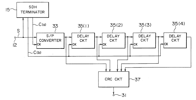
Referring now to Fig. 6 and 7, the description
will proceed to a header error check device according to
a first embodiment of this invention. In Fig. 6, similar
parts are designated by like reference symbols. Like in
Figs. l and 4, the data input terminal 12 is supplied
with an original STM signal S. The illustrated header
error check device has a single data output terminal 31.
Supplied with the path overhead and the section
overhead which are indicated by the original STM signal S
received from the data input terminal 12, the SDH
terminator or terminating circuit 15 produces a bit
control signal C(a) and a unit control signal C(b).
In the manner illustrated in Fig. 7 along a first
or top row labelled (S), the original ATM signal is not
different from that described in conjunction with Figs. l
through 5. As depicted along a second row labelled
(C(a)), the bit control signal indicates the bits of the
first through the N-th ATM cell header units of the first
through the P-th header blocks and the bits of the first
through the N-th ATM cell header error check units. In
the manner exemplified along a third row labelled (C(b))
by pulses, the unit control signal indicates successively
the first through the N-th ATM cell header units in the
first through the P-th header blocks and subsequently
19 20~9396
successively the first through the N-th ATM cell header
error check units.
A serial-parallel (S/P) converter 33 is supplied
with the original ATM signal S from the data input
terminal 12 and controlled by the bit and the unit
control signals C(a) and C(b) supplied from the SDH
terminator 15. Controlled by the bit control signal C(a)
when the unit control signal C(b) indicates the (p, n)-th
ATM cell header unit, namely, the n-th ATM cell header
unit in the p-th header block, the serial-parallel
converter 33 produces a zeroth bit-parallel signal which
represents in bit parallel the (p, n)-th ATM cell header
unit and subsequently the n-th ATM cell header error
check unit when the unit control signal C(b) indicates
the n-th ATM cell header error check unit.
First through P-th delay circuits 35(1), 35(2),
..., and 35(P) are connected in cascade to the
serial-parallel converter 33. The first through the P-th
delay circuits 35 (suffixes omitted) are for producing
first through N-th bit-parallel signals with each delay
circuit supplied with the unit control signal C(b) from
the SDH terminator 15. In this manner, a p-th delay
circuit 35(p) produces a p-th bit-parallel signal by
giving a (p-l)-th bit-parallel signal a delay which is
equal to NQ bit intervals, namely, to N times a plurality
of bit intervals, equal in number to the third
predetermined natural number Q. When p is equal to
unity, the (p-l)-th bit-parallel signal is the zeroth
-
2059396
bit-parallel signal.
When the unit control signal C(b) eventually
indicates the n-th ATM cell header error check unit, the
first through the P-th bit-parallel signals represent the
n-th ATM cell header units of the first through the P-th
header blocks in bit parallel. At this moment of time,
the zeroth bit-parallel signal represents the n-th ATM
cell header error check unit in bit parallel.
In Figs. 6 and 7, it is presumed that the first
ln predetermined natural number P is equal to four. The
delay circuits 35 are consequently designated by the
reference numerals 35(1), 35(2), 35(3), and 35(4). In
the manner exemplified in Fig. 7 along fourth through
sixth rows labelled (35(4)), (35(3)), and (33), the
fourth bit-parallel signal represents the bits A(l)
through A(8) of the first ATM cell header unit of the
first header block at a time instant after the unit
control signal C(b) indicates the first ATM cell header
error check unit. The third bit-parallel signal
represents the bits A(9) through A(16) of the first ATM
cell header unit of the second header block at the time
instant under consideration. In a like manner, the
second and the first bit-parallel signals represent the
bits A(17) through A(32) of the first ATM cell header
units of the third and the fourth header blocks. The
zeroth bit-parallel signal represents the bits AH(l)
through AH(8) of the first ATM cell header error check
unit at the time instant in question. It is now
21 2059396
understood in general that the p-th bit-parallel signal
represents the bits of the n-th ATM cell header unit in a
(P-(p-l))-th header block when the unit control signal
indicates the n-th ATM cell header error check unit.
In Fig. 6, a single cyclic redundancy (CRC)
circuit 37 is supplied with the zeroth through the P-th
bit-parallel signals from the serial-parallel converter
33 and from the first through the P-th delay circuits 35.
Carrying out the cyclic redundancy check on the zeroth
through the P-th bit-parallel signals related to the n-th
ATM cell header units of the first through the P-th
header blocks and to the n-th ATM cell header error check
unit, the cyclic redundancy check circuit 37 produces an
n-th check result signal representative of an n-th check
result among first through N-th check results which are
successively represented by first through N-th check
result signals when the unit control signal C(b)
indicates the first through the N-th ATM cell header
error check units in succession.
In the manner exemplified in Fig. 7 along a
seventh or bottom row labelled (37), the first check
result signal has high and low levels like that described
in conjunction with Figs. 1 and 2. When no header error
is found in the n-th ATM cell header units of the first
through the P-th header blocks, the n-th check result
signal is given the low level without loss of generality.
More particularly, the cyclic redundancy check
circuit 37 divides a combination of the n-th ATM cell
22 2 OS g 396
header units of the first through the P-th header blocks
and the n-th ATM cell header error check unit by the
generation polynomial and produces the n-th check result
signal which has the low and the high levels when a
residue is and is not equal to zero, respectively. In
other words, the cyclic redundancy check circuit 37
produces the n-th check result signal which has the low
and the high levels when the residue is absent and
present, respectively.
Referring to Figs. 8 and 9, attention will be
directed to a header error check device according to a
second embodiment of this invention. In Fig. 8, similar
parts are designated again by like reference numerals.
The data input terminal 12 is for receiving the original
STM signal S. The header error check device is for
supplying the data output terminal 27 with a rebuilt STM
signal of the type described in connection with Figs. 4
and 5 as the data output signal.
In Fig. 8, the SDH terminator 15 (Figs. 1 and 6)
is supplied with the original STM signal S from the data
input terminal 12. Controlled by the section overhead
and the path overhead, the SDH terminator 15 produces a
bit control signal C and a unit selection signal T. The
bit control signal is not different from that described
in conjunction with Figs. 6 and 7. The unit selection
signal will presently be described.
In the manner illustrated in Fig. 9 along a first
or top row labelled (S), the STM signal is not different
23 2059396
from that hitherto described. In the manner depicted
along a second row labelled (C), the bit control signal
indicates the bits of the first through the N-th ATM cell
header units of the first through the P-th header blocks
and the bits of the first through the N-th ATM cell
header error check units. As exemplified along a third
row labelled (T) in connection with the first ATM cell
header error check unit alone, the unit selection signal
selectively indicates the first through the N-th ATM cell
header error check units by a logic zero level.
In the header error check device being
illustrated, a clock counter 41 is supplied with the bit
control signal C from the SDH terminator 15. Counting
the bits which are indicated by the bit control signal C,
the clock counter 41 counts up a clock count one by one
from an initial value of zero whenever the bits are
counted to the third predetermined natural number Q. The
clock count is reset to the initial value as soon as the
clock count of (N - 1) is reached. The clock counter 41
thereby produces a count signal representing such clock
counts as (0, l)-th through (0, N)-th, (1, l)-th through
(1, N)-th, ..., (p, l)-th through (p, N)-th, ..., and (P,
l)-th through (P, N)-th clock counts. Each of (p, n)-th
clock counts is represented in bit parallel by the count
signal which is an equivalent of the unit control signal
C(b) described in connection with Figs. 6 and 7.
The clock counter 41 additionally produces a
write pulse sequence of negative-going write pulses
24 2059396
indicative of write-in in the manner which will shortly
be described. In the write pulse sequence, the write
pulses appear to indicate (0, l)-th through (0, N)-th,
..., (p, l)-th through (p, N)-th, ..., and (P, l)-th
through (P, N)-th write-in instants which are numbered in
correspondence to the clock counts. Each write pulse is
produced when the count signal ceases to indicate a
correspondingly numbered clock count.
In the manner illustrated in Fig. 9 along a
fourth row labelled (41-1), the count signal represents
zero through (N - 1) repeatedly as the (p, l)-th through
the (p, N)-th clock counts with the number p indicative
of successive header blocks incremented one by one at
each repetition. The write pulse sequence is depicted
without the numbers of the write-in instants along a
fifth row labelled (41-2).
In Fig. 8, a single cyclic redundancy check (CRC)
circuit 43 is supplied with the original STM signal S
directly from the data input terminal 12 and with the bit
control signal C from the SDH terminator 15. In the
manner which will presently be described, the cyclic
redundancy check circuit 43 is supplied furthermore with
a (p, n)-th previous result signal which represents at a
current time instant defined by the (p, n)-th write-in
instant a previous result obtained at a previous time
instant defined by a (p-l, n)-th write-in instant,
namely, at N times the third predetermined natural number
Q of bit intervals prior to the (p, n)-th write-in
2059396
instant.
Using the previous result signal, the cyclic
redundancy check signal 43 selects the (p, n)-th ATM cell
header unit from the original STM signals and carries out
the cyclic redundancy check on the (p, n)-th ATM cell
header unit to produce the (p, n)-th result signal of the
type described in connection with Figs. 4 and 5. More
particularly, the (p, n)-th result signal serves as a
(p, n)-th intermediate result signal representative of a
(p, n)-th updated ATM cell header error check unit as the
(p, n)-th result in bit parallel.
An AND gate 45 is supplied with the (p, n)-th
intermediate result signal from the cyclic redundancy
check circuit 43. Supplied additionally with the unit
selection signal T from the SDH terminator 15, the AND
gate 45 allow the (p, n)-th intermediate result signal to
pass therethrough as a (p, n)-th output result signal
insofar as the unit selection signal T is given a high
level depicted in Fig. 9 along the third row (T).
A random access memory (RAM) 47 is supplied with
the (p, n)-th output result signal from the AND gate 45
and has first through N-th memory cells which are
symbolically depicted at 49(1), 49(2), ..., and 49(N) and
are accessible by the (p, l)-th through the (p, N)-th
clock counts represented by the count signal supplied
from the clock counter 41. In response to the count
signal and the write pulse sequence supplied from the
clock counter 41 to indicate the (p, n)-th clock count
26 20S9396
for accessing to an n-th memory cell 49(n) and to
indicate the correspondingly numbered write-in instant,
the (p, n)-th output result signal is stored in the n-th
memory cell 49(n) as a (p, n)-th memorized result signal.
While supplied only with the count signal representatlve
of the (p, n)-th clock count, the random access memory 47
produces a (p-l, n)-th memorized result signal from the
n-th memory cell 49(n) as the (p, n)-th previous result
signal.
In the meantime, the count signal represents the
(P, n-l)-th clock count and immediately subsequently the
(P, n)-th clock count. At this instant of time, the
(P, n)-th output result signal is stored in the n-th
memory cell 49(n) as an n-th final result signal. When
the count signal represents a (P, n)-th clock count, the
random access memory 47 produces the (P, n)-th final
result signal as the n-th result signal representative of
the n-th result of the type described in connection with
Figs. 4 and 5.
It is now understood in connection with Figs. 8
and 9 that a combination of the AND gate 45 and the
random access memory 47 serves as a memory section
connected to the cyclic redundancy check circuit 43 and
controlled by the write pulse sequence which serves as
the unit control signal. When the unit control signal
indicates successively the (p, n)-th ATM cell header
units, the memory section (45, 47) memorizes the (p,
n)-th intermediate result signals as the (p, n)-th
27 2059396
memorized result signals and supplies the cyclic
redundancy check circuit 43 with the (p-l, n)-th
memorized result signals as the (p, n)-th previous result
signals to produce, when the unit control signal
eventually indicates the n-th ATM cell header error check
unit, the (P, n)-th memorized result signal as an n-th
result representative of the error correcting code
(namely, the residue) in connection with the (p, n)-th
ATM cell header units.
Briefly stated with reference to Figs. 8 and 9,
the cyclic redundancy check circuit 43 is connected to
the data input terminal 12 and to the SDH terminator 15
and is for carrying out the cyclic redundancy check, when
the unit control signal indicates successively the n-th
ATM cell header units in the first through the P-th
header blocks, on the (p, n)-th ATM cell header units and
the (p, n)-th previous result signals. The cyclic
redundancy check circuit 43 thereby produces results of
the cyclic redundancy check as the (p, n)-th intermediate
result signals with each (p, n)-th intermediate result
signal produced in bit parallel in accordance with the
bit control signal C.
Another combination of the SDH terminator 15 and
the clock counter 41 serves as a control signal producing
section. Connected to the data input terminal 12, the
control signal producing section (15, 41) produces the
bit control signal C and the unit control signal
collectively as the afore-described collective control
28 2059396
signal.
Reviewing Figs. 6 and 7 and the description so
far made with reference to Figs. 8 and 9, the header
error check device has the data input terminal 12 for
receiving the STM signal S and includes either the SDH
terminator 15 or the combination of the SDH terminator 15
and the clock counter 41 as a control signal producing
section for producing the collective control signal.
Either a combination of the serial-parallel converter 33,
the delay circuits 35, and the cyclic redundancy check
circuit 37 or another combination of the single cyclic
redundancy check circuit 43 and the memory section (45,
47) serves as a sole error checking section. Connected
to the data input terminal 12 and to the control signal
producing section (15 or 15, 41), the sole error checking
section (33, 35, 37 or 43, 45, 47) checks the header
error in connection with the n-th ATM cell header unit of
the p-th header block and the n-th ATM cell header error
check unit when the collective control signal indicates
the n-th ATM cell header unit of the p-th header block
and subsequently the n-th ATM cell header error check
unit.
Referring more particularly to Figs. 8 and 9, the
header error check device comprises a parallel-serial
(P/S) converter 51 supplied with the bit control signal C
from the SDH terminator 15 and with the n-th final result
signal from the random access memory 47 when the count
signal represents the (P, n)-th ATM cell header unit.
29 2059396
Controlled by the bit control signal, the parallel-serial
converter 51 converts the n-th final result signal to an
n-th updated ATM cell header error check unit of first
through N-th updated ATM cell header error check units.
In the manner exemplified in Fig. 9 along a sixth row
labelled (51), the first updated ATM cell header error
check unit consists of first through N-th or eighth
updated bits Ah(l), Ah(2), ..., and Ah(8).
A single selector or switch 53 is connected to
the data input terminal 12, the SDH terminator 15, the
data output terminal 27, and the parallel-serial
converter 51. When controlled by the unit selection
signal T indicative of the n-th ATM cell header error
check unit, the selector 53 substitutes the n-th updated
ATM cell header error check unit for the n-th original
ATM cell header error check unit. The selector 53
eventually supplies the data output terminal 27 with a
rebuilt STM signal in which the first through the N-th
original ATM cell header error check units are
selectively changed to the first through the N-th updated
ATM cell header error check units. In Fig. 9, the
rebuilt STM signal is depicted along a seventh or bottom
row labelled (27).
The unit selection signal T has the low level on
indicating the n-th ATM cell header error check unit. In
this event, the AND gate 45 produces a zero signal
instead of the (p, n)-th output result signal.
2059396
Referring now to Fig. 10, an ATM cell monitoring
device is an error check device according to a third
embodiment of this invention and is for use in
combination with an ATM cell transmission system 60
having system input and system output terminals 61 and
62. The system input terminal 61 is for receiving a
system input ATM cell. The ATM cell transmission system
60 is for transmitting the system input ATM cell to the
system output terminal 62 as it is. The ATM cell
transmission system thereby produces the system input ATM
cell as a system output ATM cell. The ATM cell
transmission system 60 is, for example, a
cross-connection network known in the art.
The ATM cell monitoring device is for monitoring
the ATM cell transmission system 60 to check an error in
the system output ATM cell. The ATM cell monitoring
device comprises a first format converter 71 supplied
with an original ATM cell of a preselected number of
bytes which cell typically consists of fifty-three bytes
in the manner described in conjunction with Fig. 3.
The original ATM cell is included in another
virtual container VC-4(NC) carried by another STM signal.
As is known in the art, the virtual container VC-4(NC)
comprises a path overhead POH and a succession of ATM
cells following the path overhead POH in the other STM
signal. When attention is directed to one of the
succession of ATM cells, this one of the succession of
ATM cells is referred to as the original ATM cell.
31 2059396
Controlled by another SDH terminator which is similar to
the SDH terminator 15 illustrated in Fig. 1 and is not
herein depicted, the original ATM cell is supplied to the
first format converter 71.
The first format converter 71 converts the
original ATM cell into a first converted ATM cell of the
preselected number of bytes plus an empty byte which is
illustrated in Fig. 3 as an area partly enclosed with a
dash-dot line.
Connected to the first format converter 71, a
first error checking circuit 72 checks a first error in
the preselected number of bytes of the first converted
ATM cell to produce a first error correcting code. The
first error checking circuit is typically a first cyclic
redundancy check (CRC) circuit. In this case, the first
error correcting code is a first residue given by
dividing by a generation polynomial the preselected
number of bytes of the original ATM cell included in the
first converted ATM cell.
A combiner 73 is connected to the system input
terminal 61 of the ATM cell transmission system 60, the
first format converter 71, and the first error checking
circuit 72. The combiner 73 produces a full ATM cell by
placing the first error correcting code in the empty byte
of the first converted ATM cell. The combiner 73
delivers the full ATM cell to the system input terminal
61 as the system input ATM cell.
32 2059396
A second error checking circuit 74 is connected
to the system output terminal 62 of the ATM cell
transmission system 60. The second error checking
circuit 74 checks a second error in the preselected
number of bytes of the original ATM cell included in the
system output ATM cell to produce a second error
correcting code. The second error checking circuit is
typically a second cyclic redundancy check (CRC) circuit.
In this case, the second error correcting code is a
second residue given by dividing the preselected number
of bytes in the system output ATM cell by the generation
polynomial.
Connected to the system output terminal 62 of the
ATM cell transmission system 60 and the second error
checking circuit 74, a comparator 75 carries out a
comparing operation of comparing the first error
correcting code in the system output ATM cell with the
second error correcting code to produce a result of the
comparing operation. More specifically, the comparator
75 produces, as the result of the comparing operation,
coincidence and non-coincidence signals representing
coincidence and non-coincidence between the first error
correcting code and the second error correcting codes.
Connected to the system output terminal 62 of the
ATM cell transmission system 60, a second format
converter 76 converts the system output ATM cell of the
preselected number of bytes plus the first error
correcting code into a second converted ATM cell
33 2059396
consisting of the preselected number of bytes. When the
coincidence signal is produced by the comparator 75, the
original ATM cell is correctly transmitted as the second
converted ATM cell by the ATM cell transmission system
60. When the non-coincident signal is produced by the
comparator 75, the original ATM cell is incorrectly
transmitted as the second converted ATM cell by the ATM
cell transmission system 60.
Thus, the ATM cell monitoring device can check an
error in the header and in the information field
following the header in the ATM cell.