Note: Descriptions are shown in the official language in which they were submitted.
2fl594~1
1
METHOD FOR MINIMIZING THE SWITCHING
LOSS IN A POWER SWITCH
Backgroundl of the invention
The invention relates to power switches such as power
transistors and diodes and in particular to a method
for reducing switching loss in a power switch, e.g. a
pulse-width-modulated power switch.
The switching losses constitute the major limitation
to the use of power switches at high switching fre-
quencies such as those which are required for instance
in a power converter in order to reduce the mass of
magnetic and capacitive components.
Several sn.ubber circuits have been proposed so far for
solving this important problem and among other patents
relating t:o the subject is U.S. Pat. No. 4,669,023.
However, all prior art snubber circuits have the dis-
advantage that they only have a low efficiency so that
any power loss saving of the power switch was paid for
by the inefficiency of the snubber circuit itself
resulting in little total power gain. The reasons for
the low efficiency of the state-of-the-art snubber
circuits are the following.
Generally the object of the snubber circuit was tc
relieve t:he main power switch of the voltage and cur-
rent stress associated with power switching and many
of the =~nubber circuits use very inefficient tech-
niques re~~ulting in a total decrease in efficiency.
In most prior art snubber circuits, the power switch
CA 02059457 2000-12-12
2
is used for providing the energy to the circuit, which
has a double consequence . 1) an additional stress is
put on the power switch, and 2) the power switch is
chosen with a low resistance, but this constitutes a
handicap for the switching part of its working cycle
because a low resistance is normally incompatible with
a high switching speed.
In other arrangements, the energy used by the circuit
is taken from the power supply and is returned to the
input. Hence a low total efficiency is achieved. An
example of zero voltage switching converter of this
kind is disclosed in U.S. Pat. No. 4,959,764.
Summary of the invention
It is the object of the present invention to minimize
the switching loss in power switches, with a higher
efficiency than the prior art.
In accordance with the first aspect of the invention
there is provided a method for minimizing a method for
minimizing the switching loss in at least one controlled
power switch connected in an electric circuit having an
input connected across an input voltage source and
having an output,
the method comprising the step of connecting
switching converter in parallel with the at least one
controlled power switch so that the switching converter
means is allowed to operate from the input voltage and
transfer energy from input to output of the controlled
power switch during the turn-on periods of the
controlled power switch, the step of connecting
switching converter means including:
CA 02059457 2000-12-12
3
providing transformer means having a primary
winding and a secondary winding, the primary winding
being connected in series with the switching converter
means across the input voltage,
connecting the secondary winding in series with
unidirectional switch means,
connecting the secondary winding and the
unidirectional switch means across the output of the at
least one controlled power switch,
providing capacitor means connected in parallel
with the at least one controlled power switch, and
allowing the controlled power switch to turn ON
after the switching converter means is turned ON,
whereby the controlled power switch is allowed to
turn ON with a near-to-zero voltage across it.
According to another aspect of the invention there is
provided a method for minimizing the switching loss in
at least one controlled power switch connected in an
electric circuit having an input connected across an
input voltage source and having an output,
the method comprising the step of connecting
switching converter in parallel with the at least one
controlled power switch so that the switching converter
means is allowed to operate from the input voltage and
transfer energy from input to output of the controlled
power switch during the turn-on periods of the
controlled power switch, the step of connecting
switching converter means including:
providing transformer means having a primary
winding and a secondary winding, the primary winding
being connected in series with the switching converter
means across the controlled power switch,
connecting the secondary winding in series with
unidirectional switch means,
connecting the secondary winding and the
unidirectional switch means across the output of the at
CA 02059457 2000-12-12
3a
least one controlled power switch,
providing capacitor means connected in parallel
with the at least one controlled power switch, and
allowing the controlled power switch to turn ON
after the switching converter means is turned ON,
whereby the controlled power switch is allowed to
turn ON with a near-to-zero voltage across it.
The invention may be used in numerous different con-
verter or regulator topologies, e.g. boost or buck
converter, forward converter, push-pull converter,
etc.
In the invention, the switching DC-to-DC converter is
acting as an active power switch stress relieving
means which results in minimizing the switching loss
in the snubbed power switch while providing the energy
for operation of the snubbed power switch in a very
efficient way. Further, all the energy is coupled from
input to output in a very efficient way, thereby
achieving a high total efficiency.
In addition, the invention allows pulse-width-modulat-
-, 2059457 ' ,
4
ed (PWM) converters to operate at very high frequency
and/or ei:ficiency, resulting in low-mass power sys-
tems. Also, by making the switching edges of the power
switch slower, transmission of unwanted electromagnet-
s is switch:~ng noise is reduced.
The invention will be more readily understood by ref-
erence to the accompanying drawings and the descrip-
tion to follow.
Brief description of the drawings
Figure 1 illustrates a prior art buck current regula-
tor.
Figure 2 illustrates the regulator of Figure 1 with
the invention incorporated therein.
Figures 3 to 8 illustrate the operation of the appara-
tus repre;~ented in Figure 2.
Figures 9, 10 and 11 illustrate the application of the
invention to three other typical exemplary converters.
Description of exemplary embodiments of the invention
The invention will be described when used in a conven-
tional buck current regulator as represented in Figure
1. Such a regulator comprises a pulse width modulated
(PWM) power switch S1 that controls the magnitude of
the current flowing through the inductor Lo according
to the required output voltage Vo across the output
port or according to the required output current Io.
Switch Sl is shown by way of example by a transistor
fed by a voltage source Vs connected across the input
port of the apparatus. The unidirectional switch D1
.._ ~p~~:~~7
(e.g. a diode) provides a path for the current in
inductor L,o when switch S1 is OFF. Power switch S1 is
turned ON or OFF in response to control pulses applied
to its control electrode or gate.
5
Switch Sl. has finite turn-off and turn-on times and
diode D1 causes a reverse recovery current to flow
through it when turned OFF. The result of these non-
ideal conditions during the switching transitions of
switch Sl_ is that the current through it and the
voltage across it exist simultaneously, which causes a
loss in the switch. This switching loss is proportion-
al to the frequency and is thus a major limitation to
high frequency operation.
The exemplary circuit described herein above is modi-
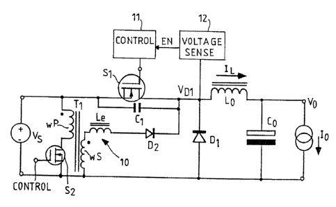
fied according to the invention as shown in Figure 2.
The modij=ication consists in connecting a low power
switching DC-to-DC converter 10 in parallel arrange-
ment with the controlled power switch S1 so that it is
allowed to operate from the input voltage and transfer
energy from input to output during the switching pe-
riods of -the controlled power switch Sl. The purpose
of the :witching converter 10 is to set the voltage
across the power switch S1 to be near to zero during
its turn-on (rise of current) and turn-off (fall of
current) periods, thereby significantly reducing the
switching loss.
In the exemplary embodiment of Figure 2, the switching
converter 10 comprises a transformer T1, the primary
winding wP of which is arranged in series connection
with a controlled switching device S2 (here shown as a
transistor) across the input voltage Vs. The secondary
winding wS of transformer T1 is arranged in series
6
2059457
connection. with a unidirectional switch D2 (here shown
as a diode:). Also included is a capacitor C1 connected
across po~~er switch S1.
The operation of switching converter 10 is illustrated
by Figures 3 to 8 . Figure 3 shows typical waveforms
in the arrangement of Figure 2 and Figures 4 to 8 show
the current paths being set in the arrangement during
five successive time periods.
Period to-~_tl (Figure 4)
It will be considered that main switch S1 is OFF and
the inductor current ID1 is flowing through diode Dl.
Before sw~_tch S1 is turned ON, switch S2 is turned ON
at time to. A current Iws flows through the secondary
winding of transformer T1 and through diode D2. Be-
cause of the equivalent inductance Le of transformer
T1, that current builds up in a linear way starting
from zero at a rate of nVs/Le (where n is the ratio of
numbers of secondary to primary turns of T1) until it
equals the value IL of the current flowing in the
inductancE~ Lo at time tl.
Period tl~-_t2 (Figure 5)
The secondary winding of transformer T1 provides all
the current IL, the current through diode D1 becomes
zero and D1 turns OFF, thereby allowing the voltage
VD1 acro:~s its terminals to rise. Since the current
Iws builds up at a controlled rate, the turn-off of
diode D1 is made soft, i.e. the reverse recovery
current is near to zero. Because switch S2 is still
ON, the ~~urrent Iws continues to flow and the voltage
across caypacitor C1 decreases to zero at time t2. The
discharge of C1 is sinusoidal in nature due to the
resonance of C1 and Le. At time t2, if the current Iws
X059457
is still greater than IL, the excess current will try
to raise the voltage but this cannot happen because
the anti-x>arallel intrinsic diode of switch S1 clamps
this voltage to the input voltage Vs.
Period t2-~t3 (Figure 6)
At time t:2, with near zero voltage across S1, this
switch can be turned ON with a very low switching
loss. Between times t2 and t3, the current Iws falls
to zero and at time t3, switch S2 is turned OFF with
only a smell current through it. Since both the turn-
on and turn-off of switch S2 occur with low values of
conducted current its switching loss can be made very
low. The sum of the currents Iws and Isl equals the
instantaneous value of current IL, the current Isl
through snitch S1 builds up from zero at a rate equal
to the fall of current Iws.
Period t3-t4 (Figure 7)
Between times t3 and t4, the current in the secondary
winding of T1 is zero and switch S1 conducts the cur-
rent IL.
Period t4-t5 (Figure 8)
At time t4, switch S1 is turned OFF. The current IL is
then provided by capacitor C1. The voltage Vsl across
the switch Sl falls from the value Vs to zero at time
t5 when diode D1 turns ON. During the turn-off of
switch S1., capacitor C1 provides most of the current
IL, so that the loss during the turn-off of S1 is kept
very low.
It is apparent from the foregoing description of oper-
ation that the power switch S1 should be allowed to
switch only when the voltage across it is near to
_ 2059457
8
zero, which happens if the voltage across diode D1
equals the value of the input voltage Vs. Referring
again to Figure 2, the switch S1 is thus controlled by
suitable control means 11 arranged to generate a con-
s trol pulsE: in response to an enabling pulse EN. Said
enable pulse is produced by a voltage sense device 12
connected for measuring the voltage VDl across diode
D1 and f:or producing said enabling pulse when the
voltage VD1 has reached the input voltage value Vs.
Figure 3 shows that switch S2 is turned ON first and
when the voltage across main switch S1 is near to
zero, sw~_tch S1 is allowed to turn ON in a lossless
way.
An advani=age in using a switching current converter
according to the invention resides in that all the
power of 1_he converter is being coupled from the input
to the oui=put, thereby to result in achieving a high
total efficiency.
In addition, the current converter provides protection
of the voltage source Vs automatically in case of
failure of diode D1. As a matter of fact, when the
diode D1 ~~auses a short circuit of the voltage source,
the outp~st voltage VDl is zero and the voltage sense
device 12 inhibits switch Sl to turn ON as explained
hereabove. Thus, no short circuit of the supply volt-
age Vs can occur as it happens in the prior art ar-
rangements, wherein it is the usual practice to ar-
range two redundant diodes D1 in series for more
failure tolerant operation. Deleting the extra diode,
in accor3ance with this invention, also provides an
increase in efficiency.
2059451
9
The embodiments described above are intended to be
exemplary and it is to be noted that the invention may
be applied to numerous other converter topologies,
e.g. boost converter, forward converter, push-pull
converter. For example, Figure 9 shows the circuit of
a typical boost converter comprising the invention.
The switching converter 10 therein operates in a simi-
lar way to that for the buck converter of Figure 2
except t'nat now it is the input current of converter
10 that forces the voltage across main switch S1 to be
zero just before it is turned ON. The waveforms are
similar to those shown in Figure 3. Figure 10 shows
the circuit of a typical forward converter comprising
the invention. Figure 11 shows the typical circuit
(known pe:r se) of a PWM push-pull converter comprising
the invent=ion. This arrangement comprises a transform-
er T2 and two power switches S1 and S1'. According to
the invention, in parallel with each power switch
there is arranged a switching converter 10, 10' as
shown in Figure 9. Each active switching converter
controls the corresponding power switch as described
hereabove and serves as a stress relieving means for
that power switch.
In view of: the above disclosure, modifications, varia-
tions and equivalent arrangements will be obvious to
one havincl ordinary skill in the art without departing
from the ~~cope of the invention.