Note: Descriptions are shown in the official language in which they were submitted.
20594S4
The present invention relates to a serial data receiving
apparatus which is appropriate to receiving serial data
having an inferior SN ratio as in a radio data communication
through weak radio waves.
As a conventional example of such a serial data
receiving apparatus, an asynchronous system receiver has been
known. The asynchronous system is arranged so that as shown
in Fig. 9, a trailing edge of a signal (point P) is assumed
as a signal start point, and an sampling signal is input at
10 the centers (C1, C2, C3, ) of the bits where predetermined
lag times (tl, t2, t3, ...) respectively have passed from the
signal start point. The P point means a point where the bit
synchronization is established.
In the conventional arrangement of the serial data
receiving apparatus, however, it is impractical to establish
the bit synchronization in the condition that the SN ratio of
the data is so inferior as often bringing about noise on the
data, because it is impossible to determine the actual
trailing edge of the signal from the trailing portion
resulting from the noise. Furthermore, though the use of a
kind of means
205946~
1 may establish the bit synchronization, the erroneous
data inputting cannot be prevented if noise is located
at the input point of the sampling signal.
For the conventional means for overcoming such
a shortcoming, a noise filter has been often used. The
filter serves to separate the noise from the signal in
light of the frequency. It means that the ideal noise
filter is arranged to enter the frequency components of
the data itself and block the other frequency
components. However, even such an ideal noise filter is
~ncapable of preventing the noise having the same
frequency components as the data. Hence, the use of the
noise filter is not so effective in overcoming the
shortcoming resulting from the noise.
As another method, there has been proposed a
method for separating the signal from the noise by
- overlapping signals on time. In the field of satellite
communication, there has been practically employed the
method where a satellite transmits a signal again and
again and a receiving apparatus on the earth adds the
same signals transmitted from the satellite again and
again and computes an average value of the added
signals. The use of this method makes it possible to
practically eliminate the adverse effect of the random
noise components and restore a vivid signal.
To realize this method, a large-volume memory
is required for temporarily storing the data transmitted
from the satellite. Further, a high-speed processor is
205946~
1 required for adding and averaging these data signals.
In case that the budget disallows the use of an
expensive high-speed processor, it takes a long time to
do the computation. Hence, it is impractical to apply
this technique to domestic equipment in light of the
` cost~and this technique cannot realize a real-time
signal-transmitting facility like a remote control unit
provided in the domestic equipment. The additional
disadvantage of this technique is that since the same
data signal is fired to the same space again and again
for transmitting one piece of data, the transmitted data
occupies the space during the signal-transmitting time
and no other data is allowed to be transmitted. Fig. 10
is a sketch illustrating a remote control system of a
spontaneous gas water heater to which the present
invention applies. A gas water heater 101 is normally
installed outside of wall or in a machine chamber. In
the gas water heater 101, the gas supplied from the gas
supply pipe 102 is combusted for heating the water
supplied from a water pipe 103. The hot water is
supplied through a hot water pipe 104 to a shower 107
located in a bathroom 105 or a faucet 108 provided in a
kitchen 106. The bathroom 105 or the kitchen 106
provides remote control units 109 and 110 by which the
hot water temperature is adjusted. The operation
signals of the remote control units 109 and 110 are
converted into radio signals 111, 112 and then are
transmitted to ~ gas water heater 101 located behind
2059464
walls 113 and 114. Conversely, the signal indicating a
driving state signal of the gas water heater 101 is
transmitted as a radio signal (not shown) to the remote
control units 109 and 110. The driving state is indicated on
an indicator. In case that the walls 113 and 114 contain a
certain kind of metal material or the gas water heater 101 is
located far apart from the bathroom 105 or the kitchen 106,
the radio signals 111 and 112 become attenuated until they
reach the bathroom 105 or the kitchen 106. This results in
making the SN ratio of the signal inferior when the receiver
(not shown) of the gas water heater 101 receives the signal.
As set forth above, the present invention is designed in
the consideration that the receiver for receiving a serial
data signal containing noise components on real time is
applied to a relatively inexpensive commodity. For example,
the present invention may apply to a home automation system
including a security facility or a portable telephone in
addition to the aforementioned remote control system of the
domestic equipment or the home.
The present invention provides a serial data receiving
apparatus which is capable of receiving a serial data signal
containing noise, that is, having an inferior SN ratio
positively and in real time.
Further, the present invention provides establishment of
bit synchronization for receiving the serial data signal
having an inferior SN ratio just on timing.
-- 4
2059464
The present invention also provides determination of a
bit logic for accurately determining a logic of each 1 bit
contained in the received serial data signal having an
inferior SN ratio.
Moreover, the present invention provides an inexpensive
serial data receiving apparatus having the foregoing
functions which employs such simple arrangement as being
applied to the domestic equipment.
The serial data receiving apparatus according to the
present invention is arranged to divide a one-bit length of
the serial data into several blocks and rapidly enter
sampling data at multiple points of each block by using a
shift register. This process is continued for extension of
several bits. The data at the same number block of each bit
is accumulated for cancelling the noise components, thereby
leaving the original signal components. The overlapping type
receiving system can clearly establish the receiving phase of
a preamble signal for bit synchronization, said preamble
signal transmitted prior to the data signal, and accurately
take bit synchronization. Based on the receiving timing
points established on the bi-t synchronization, the shift
register serves to input the sampling data signal at the
multiple points. Then, the logic value of the bit is
determined on the ratio of the number of the input data "1"
to that of "0". In addition to the process for inputting the
205q 4 64
sampling data at the multiple points through the use of the
shift register, the present invention can provide simple
arrangement for speeding up the calculation of the number of
"1" or "O" through the use of reference instructions of a ROM
table contained in a microcomputer. Moreover, the invention
can more effectively realize the accuracy by utilizing the
reversal symmetry about a first half and a later half of bi-
phase codes.
As set forth above, the present invention can provide an
inexpensive and highly-efficient serial data receiving
apparatus which uses a one-chip microcomputer having a shift
register built therein without having to use an expensive
circuit system such as a special filter or a phased lock
loop.
The invention will be described in more detail with
reference to the accompanying drawings, in which:
Fig. 1 is a block diagram showing a serial data receiver
according to an embodiment of the present invention;
Fig. 2 is a waveform view showing a signal used in the
serial data receiver;
Fig. 3 is a waveform view showing another signal used in
the serial data receiver;
Fig. 4 is a timing view showing an operation executed in
the serial data receiver;
Fig. 5 is a timing view showing another operation
executed in the serial data receiver;
-- 6 --
2059464
Fig. 6 is a timing view showing another operation
executed in the serial data receiver;
Fig. 7 is a timing view showing another operation
executed in the serial data receiver;
Fig. 8A is a flowchart showing another operation
executed in the serial data receiver;
Fig. 8B is a flowchart showing another operation
executed in the serial data receiver;
Fig. 8C is a flowchart showing another operation
executed in the serial data receiver;
Fig. 9 is a timing view showing an operation executed in
the prior art;
Fig. 10 is a sketch illustrating the domestic equipment
to which the present invention applies; and
Fig. 11 is a graph showing data about the performance
comparison between a wave signal receiver of the invention
and a wave signal receiver of the prior art.
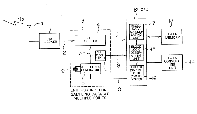
A serial data receiver according to an embodiment of the
present invention is illustrated in a block diagram of Fig.
1. 1 denotes a pre-processing unit for receiving serial
input data, which serves to
,l~;,
2059464
1 convert a preamble signal for bit synchronization
transmitted from a serial data transmitter (not shown)
and a data signal following the preamble signal into a
baseband serial data signal 2. As an example, consider
that the pre-processing unit 1 is assumed as a FM
receiver and a FM-modulated radio signal lo is trans-
mitted from the serial data transmitter. The radio
signal lo is caught by an antenna la and the FM receiver
1 serves to modulate the radio signal lo into an
original baseband type digital signal.
Fig. 2 shows an embodiment of the serial data
signal 2. In Fig. 2, an A part denotes a preamble
signal for bit synchronization and a B part denotes a
data signal. The preamble signal can be formed by
continuous transmission of the bi-phase codes. An
interval T corresponds to one bit of the bi-phase code.
Turning to Fig. 3, (a) denotes a logic 1 of the bi-phase
code and (b) denotes a logic 0. In case that such a bi-
phase code is transmitted as a radio signal, the
transmission frequency at the high-level part 18 of the
bi-phase code can be modulated to fl and the transmis-
sion frequency at the low-level part 19 can be modulated
to f2.
Returning to Fig. 1, 3 denotes a unit for
inputting sampling data at the multiple points. The
unit 3 is arranged to have a shift register 4, a shift
clock generator 5, and a shift clock counter 6. The
serial data signal 2 is input to the shift register 4 at
2059~6~
1 the sampling points as being synchronized with the shift
clock signal 7 output from the shift clock generator 5.
The counted pieces of sampling data are input and held
in the shift clock counter 6. The shift clock counter 6
is arranged to output a signal indicating completion of
a shifted input 8 when the shift clock signals 7 corre-
sponding to the number of bit of the shift register 4
are input to the shift clock counter 6.
The shift clock generator 5 serves to properly
divide an original oscillating frequency produced by a
crystal oscillator 9 and produce a shift clock signal of
a period ~tl. The generation/stop of the shift clock
signal is controlled by a shift clock control signal 10
sent from a CPU 12. That is to say, the CPU 12 enables
the shift clock generator 5 in response to the shift
clock control signal 10, when the shift clock signal 7
is generated to start the serial data signal receiving
process of the shift register 4. Then, the CPU 12
determines that the sampling input operation at multiple
points is terminated when the shifted-input complete
signal 8 is received and reads the sampling data signal
11 .
Fig. 4 is a timing view showing operation of
the unit 3 for inputting the sampling data at multiple
points. In Fig. 4, (a) denotes a preamble signal
portion of the serial data signal. (b) denotes a shift
clock signal 7 and (c) denotes a shifted-input complete
signal 8.
2059~64
1 In this embodiment, the number of bits of the
shift register 4 is assumed as 8. When eight shift
clock signals 7 are fired, the shifted-input complete
signal 8 is output. During the period of one bit of the
preamble signal, six shifting input complete signals 8
are output. One bit of the preamble signal is divided
into six blocks~and the sampling data at the eight
points are captured for each block and are read in the
CPU 12. For example, at the block No. 1 of the k-th
bit, the sampling data is "00000000". At the block No.
2, the sampling data is "00011111". At the block No. 3,
the sampling data is "11111111". Hence, the period ~tl
of the shift clock signal 7 corresponds to a time
represented by dividing one-block length by the number
of bits of the shift register 4 (in this embodiment, 8).
Again, turning to Fig. 1, a data memory 13
serves to temporarily store the sampling data read from
the shift register 4 by the CPU 12. The stored sampling
data is arranged according to each bit number and each
block number.
14 denotes a data converting unit, which
serves to calculate the number of "1" or "0" composing
the sampling data read by the CPU 12. For example, for
the input data of "00011111", the number of "1" is
output as 5 (the number of "0" is output as 3).
In addition, the data memory 13 stores the
sampling data read from the shift register 4 as it is or
as the number of "1" or "0" converted from the sampling
-- 10 --
2059464
1 data by the data converting unit 14.
17 denotes a block data accumulating unit,
which serves to accumulate the number of "1" or "0" of
the sampling data calculated by the data converting unit
14 for each block number. The accumulated value is
always updated such as the latest 10 bits.
In turn, 15 denotes a block logic determining
unit, which serves to determine the logic value of each
block from the accumulated value of the input data "1"
or "0" of each block number obtained by the block data
accumulating unit 17. Table la shows the principle on
which the block logic is determined and the embodiment
in case of 1 bit. In actual, for example, 10-bit blocks
are accumulated for determining the block logic based on
the specification shown in Table lb. The logic
determination can be easily realized by the program run
in the microcomputer.
Table la Table lb
Number of Block logic Number of Block logic
data 1 value data 1 value
O O
1 0 0 ~ 27 0
2 0
3 Undefined
4 Undefined 28 ~ 52 Undefined
Undefined
7 - 1 53 ~ 80
-- 11 --
205946~
1 16 denotes a unit for establishing bit
synchronization, which serves to obtain the phase
relation between the preamble signal being input and the
receiving timing of the CPU 12 from the serial patterns
of the block logic value from the blocks No. 1 to No. 6
obtained by the block logic determining unit 15 and to
establish the bit synchronization timing. This process
can be easily realized by the program run in the
microcomputer. Table 2 shows the specification of the
phase relation and the serial patterns of the block
logic values. The specification corresponds to the
timing view of Fig. 5.
The line of the serial pattern number 1 in
Table 2 indicates the case where the block logic values
of the blocks Nos. 1 to 6 have the serial pattern of
[1], [1], [1], [0], [0] and [0]. The phase lag between
the data signal and the receiving timing in the CPU 12
is defined as 0. Hence, this pattern is a reference on
which the block logic values indicate another serial
pattern. The timing of this case corresponds to a part
(a) of Fig. 5. Then, the line of the serial pattern
number 2 of Table 2 indicates the case where the block
logic values have the serial pattern of [undefined],
[1], [1], [undefined], [0] and [0]. It indicates the
receipt of the data signal lags behind the reference by
1/12 bit. The timing of this case corresponds to a part
(b) of Fig. 5. The serial patterns of the block logic
values indicated in Table 2 respectively correspond to
- 12 -
205946~
1 parts (c) to tl) of Fig. 5 in the similar manner as
above. ~T of Fig. 5 indicates the processing error of
the bit synchronization timing caused in the [undefined]
part of the block logic value definition of Table l. In
this embodiment, the timing error is at most +l/24 bit.
To lessen the error, it is possible to increase the
blocks in number.
- 13 -
2059464
Table 2
Serial Block No Relative Corre-
pat- phase sponding
tern lcgparts of
No. 1 2 3 4 5 6 ~qg Fig. 5
1 1 1 1 0 0 0 0 (a)
2 x 1 1 x O O 1 (b)
3 0 1 1 1 0 o 2 (c)
4 0 x 1 1 x 0 12 (d)
0 0 1 1 1 0 4 (e)
6 0 0 x 1 1 x 12 'f'
7 0 0 0 1 1 1 6 (g)
8 x O O x 1 1 7 (h)
9 1 0 0 0 1 1 8 (i)
1 X O O x 1 9 ( j )
11 1 1 0 1 10 (k)
12 1 1 x x 11 (1)
x denotes "undefined"
2059464
1 As set forth above, the present invention is
designed to accumulate the sampling data corresponding
to several bits of the preamble signal for each block
number (that is, for each phase) and determine the block
logic based on the accumulated data for the purpose of
eliminating the random adverse effect of the noise and
precisely determine the block logic based on the
original signal components. Further, the preamble
signal and the phase relation of each block, that is,
the receiving timing,are sensed by the serial pattern of
the block logic values obtained by the above manner for
the purpose of establishing the bit synchronization
timing. The established bit synchronization timing is a
reference timing on which the preamble signal and the
serial data thereafter are received. It results in
making it possible to establish very accurate and stable
bit synchronization against a low SN signal.
Next, another embodiment of the present
invention will be described. As is obvious from Fig. 4,
by using the bi-phase code as a preamble signal, at each
combination of the first block and the fourth block, the
second block and the fifth block and the third block and
the sixth block, the input data is made to be the same
in the ideal state with no noises merely by reversing
the logic of the input data.
The other block logic determining unit 15 of
this invention provides arrangement for providing a
block logic by relating the data at the-i-th block to
20~946~
1 the block data at the (i+n)th block, wherein the number
of the divided blocks is 2n (n is a natural number) and
i is an integer meeting the relation of l~i~n. Table 3
shows the principle on which the block logic is
e~
determined. The shown embodiment concern~ with one bit.
In actual, the block logic is determined by accumulating
the blocks corresponding to ten bits. Hence, the number
of "1" has a value corresponding to 10 bits for the
determination.
Table 3
\ Number of logic "1" at (i+n)th block
\ O 1 2 3 4 5 6 7 8
o x x x x o o o o o
x x x x x o o o o
Number 2 x x x x x x O O O
logic 3 x x x x x x x O O
"1" at
the 4 1 x x x x x x x O
block 5 1 1 x x x x x x x
6 1 1 1 x x x x x x
7 1 1 1 1 x x x x x
8 1 1 1 1 1 x x x x
x denotes "undefined"
Another embodiment of the block logic
determining unit 15 provides arrangement for determining
a logic of the block based on the i-th block data and a
reversed value of the (i+n)th block data. Table 4 shows
the specification for determining the phase relation
- 16 -
20S946!1
1 between the serial pattern and the preamble signal based
on the block logic value as h~in~ related to Fig. 5
Table 4
Serial Block No Relative Corre-
pat- phase sponding
tern 143 parts of
No. 1(4) 2(5) 3(6) ~a~ Fig. 5
1 1 1 1 0 (a)
2 undefined 1 1 1 (b)
3 0 1 1 2 (c)
4 0 undefined 1 3 (d)
0 0 1 4 (e)
6 0 0 undefined 5 (f)
7 0 0 o 162 (g)
8 undefined O 0 7 (h)
9 1 0 o 8 (i)
1 undefined O 9 (j)
11 1 1 0 10 (k)
12 1 1 undefined 11 (1)
- 17 -
2059464
1 As described above, if the logic determination
is carried out on the basis of the i-th block data and
the (i+n)th block data of the accumulated block data
corresponding to the latest predetermined bits, the
logic is determined on the doubled data, so that the bit
synchronization can be established very accurately and
stably. This embodiment ~a4 concerned with the case of
2n=6, that is, n=3~wherein one bit of the preamble
signal is divided by six blocks.
As described in the foregoing embodiments, the
preamble signals composed of bi-phase codes are
accumulated for each block number of each bit. Since
the block logic is determined on the accumulated block
data, the accurate bit synchronization can be
efficiently realized.
Next, the method for receiving the preamble
signal and the data signal thereafter and determining
the logic of these signals will be described with
reference to Fig. 6. In Fig. 6, a part (a) denotes a
serial input signal 2, a part (b) denotes a shift clock
signal 7, a part (c) denotes a shifted-input complete
signal 8, a part (d) denotes a shift clock control
signal 10. An A point in Fig. ~ is a synchronization-
establishing point obtained by the foregoing process.
With this A point as a reference point, the sampling
input is done for each bit of a data signal. Then, the
shift clock generator 5 is started at the points Bl, B2,
B3, ... . Those are respectively the points where
- 18 -
20~946~
1 predetermined lag times tl (corresponding to ~T/2 or
more of Fig. 5 for eliminating the adverse effect of the
processing error of the bit synchronization timing),
tl+ta, tl+2ta, ... pass from the A point. With the
shift clock generator 5 being started, the input data is
automatically input to the shift register 4. ta denotes
a l/2 bit length of the serial input signal 2. The
generating time tb of the shift clock signal 7 is made
to be (ta-~T) or less. The period ~t2 becomes:
At2=tb/number of bits of shift register (8 in
this embodiment)
The foregoing arrangement makes it possible to
do the sampling data corresponding to the number of bits
of the shift register 4 as eliminating the adverse
effect of the synchronization-establishing error (~T/2)
during the interval of the serial input data l/2 bit.
In addition, Fig. 6 shows the embodiment where the data
is input when the bi-phase codes are used as the serial
input data. In Fig. 6~hence, the sampling data
corresponding to the number of bits of the shift
register 4 is input for each l/2 bit of the data signal.
However, it goes without saying that this invention is n~
~ n
limited to this embodiment and also includes arrangement
for entering the sampling data corresponding to the
number of bits of the shift register 4 during the one-
bit length of the data signal.
-- 19 --
20S9464
1 After the shift clock signal 7 corresponding
to the number of bits of the shift register 4 is output,
the shifted-input complete signal 8 is output to the CPU
12 on the timing as shown in Fig. 6(c). The CPU 12
serves to control the shift clock control signal 10 on
the timing shown in Fig. 6(d). Hence, the CPU 12 is
capable of doing another work during the tb period when
at least the shift clock control signal 10 is being
output without having to do the receiving process.
The method for inputting a data signal and
determining the logic of the data signal will be
concretely described with reference to Fig. 7. The
parts (a) and (b) of Fig. 7 indicate a one-bit serial
data signal composed of bi-phase codes output from the
serial data pre-processing unit 1 such as the FM
receiver and input to the shift register 4. The part
(a) of Fig. 7 indicates an ideal data signal with no
noise. The part (b) exemplarily shows a signal input
with the noise. By supplying the shift clock signal (C)
output from the shift clock generator 5 to the shift
register 4, it is possible to determine the timing on
which the serial data shown in the parts (a) and (b) of
Fig. 7 is entered as sampling data at the multiple
points.
The number of sampling inputs is defined by
the number of bits of the shift register 4. In this
embodiment, the number is 8. The input data of 8
samples can be obtained respectively at the first half
- 20 -
2059464
1 and the second half of the bi-phase codes on the timing
shown in Fig. 7. In Fig. 7, a point Bl is a sampling
start point of the bit first half defined from the
reference point obtained by the foregoing bit-
synchronizing process. A point B2 is a sampling startpoint of the second half. The time from Bl to B2 and
the time ta from B2 to the sampling start point B3 of
the first half of the next bit are determined depending
on a data transmission speed.
The shift clock signal 7 in Fig. 7(c) is
controlled by the shift clock control signal 10 sent
from the CPU 12. After the shift clock signal 7 corre-
sponding to the number of bits of the shift register 4
(8 in this embodiment) is output, the shifted-input
complete signal 8 is supplied to the CPU 12. When the
shifted-input complete signal is input, the CPU 12
determines that the sampling input at the multiple
points is terminated, reads the sampling data held in
the shift register 4 through the data bus 11 and
determines the logic of the bit based on the read data.
For example, the sampling data in the state of the ideal
input data is composed of "11111111" at the first half
and "00000000" at the second half. As shown in Fig.
7(b), however, the input data containing noises thereon
is composed of "10110010" at the first half and
"01000010" at the second half.
Next, from the sampling data, the number of
"1" or "0" contained in the data is calculated by the
- 21 -
205946~
1 data converting unit 14. For example, in case of the
input data shown in Fig. 7(a), the number of "1" at the
~ ~'rs2;
first half is 8, the number of "O" at the ~ccond half is
0, the number of "1" at the second half is 0, and the
number of "O" at the second half is 8. As in Fig. 7(b),
the number of "1" at the second half is 4, the number of
f ,'~ s ~
"O" at the ~ccond half is 4, the number of "1" at the
second half is 2, and the number of "O" at the second
half is 6.
The data converting unit 14 provides a data
conversion table as shown in Table 5. That is to say,
the data input and held to the shift register 4 is
assumed as an input value~and the number of "1"
contained in the input value is output.
Table 5
Input value Output value
(Sampling data) (Number of
logic "1")
O O O O O O O O O O
0 0 0 0 0 0 0 1
2 0 0 0 0 0 0 1 0
3 0 0 0 0 0 0 1 1 2
4 0 0 0 0 0 1 0 0
0 0 0 0 0 1 0 1 2
6 0 0 0 0 0 1 1 0 2
.
;
253 1 1 1 1 1 1 0 1 7
254 1 1 1 1 1 1 1 0 7
255 1 1 1 1 1 1 1 1 8
205946~
1 In this embodiment, since the number of bits
of the shift register 4 is 8, it is necessary to prepare
256 data table areas. That is to say, the input value
is an 8-bit address and the output value corresponding
to each address (input value) is stored in a memory area
(ROM). Hence, by specifying the address with the input
value, it is possible to immediately obtain the number
of "1" contained in the output value, that is, the input
value.
If the resulting output value is more than a
predetermined reference, therefore, the input data is
determined as a logic "1". If it is less than the
reference, it is determined as a logic "0". If the
output value is out of the reference, it is determined
~5C
as "undefined". In actual, the data conversion table
can be easily realized by using the ROM table reference
instructions of the microcomputer. The shift register
4, the shift clock generator 5 and the shift clock
counter 6 can be implemented to have simple and
inexpensive arrangement if the microcomputer having
their functions on a single chip is used.
In turn, the foregoing data inputting process
and the logic determining process will be described with
reference to the flowchart for executing the program of
the CPU 12.
In Fig. 8A, 20 denotes bit-synchronizing
process. The sampling input unit 3 operates to
establish the reference point on which the sampling
- 23 -
205946~
1 start point is determined. 21 denotes the sampling
process at the multiple points of the first and the
second halves by starting the shift clock generator 5.
22 denotes a process which reads the sampling data from
the shift register 4 and calculatesthe number of "1"
contained in the data through the shift register 4. 23
denotes a process which determines the logic of the bit
based on the number of "1" obtained by the data
converting unit 14.
With reference to Figs. 8B and 8C, the first
and the second algorithms for determining the bit will
be described. The first algorithm shown in Fig. 8B is
configured on the idea that if one of the first half and
the second half of the bi-phase codes contains noises,
the logic of the bit is established if the other half
holds the accurate data. The second algorithm shown in
Fig. 8C is configured on the idea that if both of the
first and the second halves contain noises, the logic of
the bit is determined by the accumulated values of the
data of the first half and the logically reversed value
of the data of the second half.
Both of the algorithms are configured to
determine the logic of the bit based on the reversal
symmetry of the bi-phase codes by using the sampling
data of the first half and the second half. In the
process shown in Fig. 8B, at a step 24, it is determined
whether or not the number of "1" at the first half of
the sampling data is 7 or more. If yes, at a step 25,
- 24 -
20~9464
1 it is determined whether or not the number of "1" at the
second half is 4 or less. In this embodiment, the
sampling number is 8. Hence, if the number of "1" at
the second half is 4 or less, the logic of the bit is
determined as "1". If it is 5 or more, the logic of the
bit is determined as "undefined". The "undefined" is
prepared for preventing erroneous determination if the
difference between the data at the first half and at the
second half is reduced to zero. The determination of
bit logic at the steps 26 to 31 is carried out in the
same manner as above. Table 6 shows the specification
for determining the bit logic according to the first
algorithm.
Table 6
\ Number of logic "1" at second half
\ O 1 2 3 4 5 6 7 8
o x x x x o o o o o
x x x x o o o o o
of 2 x x x x x x x O O
logic 3 x x x x x- x x o O
"1" at
first 4 1 1 x x x x x 0~ x
half 5 1 1 x x x x x x x
6 1 1 x x x x x x x
7 1 1 1 1 1 x x x x
8 1 1 1 1 1 x x x x
x denotes "undefined"
- 25 -
20S946~
1 At the process of Fig. 8C, at a step 32, the
number of values of "1" at the first half is added with
the number of reversed values of "1", that is, values of
"O" and the added values are accumulated. Then, at
steps 33 and 34, it is determined whether the
accumulated value is 11 or more or 5 or less. If it is
11 or more, the logic value of the bit is determined as
"1" and if it is 5 or less, the logic value of the bit
is determined as "O". If it belongs to the range except
the above ranges, the logic of the bit is determined as
"undefined". Table 7 indicates the specification for
determining the bit logic based on the second algorithm.
Table 7
\ Number of logic "1" at second half
\ O 1 2 3 4 5 6 7 8
o x x x o o o o o o
x x x x o o o o o
of x x x x x o O O O
logic 3 1 x x x x x o O O
"1" at
first 4 1 1 x x x x x O O
half 5 1 1 1 x x x x x o
6 1 1 1 1 x x x x x
7 1 1 1 1 1 x x x x
8 1 1 1 1 1 1 x x x
x denotes "undefined"
In the above description, the number of
sampling inputs has been defined as 8, but this
- 26 -
205946a~
1 invention is not limited to this defined number. The
reference numerical values for determining the logic of
a bit are not defined to the values described in the
above embodiment.
In turn, the effect of the invention will be
described with reference to the experimental data.
Fig. 11 shows the data about compared
performances between the receiver developed according to
the present invention and the receiver employing a
conventional filter system. The conventional receiver
uses a remote control encoder IC made by Motorola,
MC145026 as a transmission control unit of the
~e code ~
transmitter and a remote control cncodcr IC made by
Motorola, MCl45027 as a receipt control unit of the
receiver. This decoder MC145027 includes two RC
filters. The time constant of the first filter is set
to be longer than a one-bit length of a signal
transmitted from the encoder MCl45026 and serves to
detect the termination of signal packets being
transmitted. The first filter is capable of removing a
single-shot noise. The time constant of the second
filter is set to determine the signal of "l" from that
of "0", both of the signals having respective pulse
widths. The second filter, therefore, serves to remove
the noises having the different pulse widths from those
of the signal "1" or "0".
In the foregoing conventional receiver and the
system of this invention, the data was transmitted from
- 27 -
2059464
1 both of the transmitters 1000 times~and the receipt
ratio of each receiver was measured. The receipt ratio
means a ratio of the accurately received data to the
other data. In addition, the measurements were carried
out as varying the strength of a radio signal fired by
the transmitter. According to the measured data, the
system developed by the invention can offer more
performance by about 6 dB than the conventional system.
In general, the attenuation of a radio signal is
inversely proportional to the distance. The 6 dB more
receipt performance means that the travel of a radio
signal is doubled. It means that this power-up is very
effective.
As set forth above, the present invention can
offer a quite useful serial transmission system
implemented by an inexpensive one-chip microcomputer
having a shift register built therein.
- 28 -