Note: Descriptions are shown in the official language in which they were submitted.
e.. ;,~r C.~ ~~
~~~~~~~t
~.CT'fLE OF THE INVEN~CION
SPREAD SPECTRUM SIGNAL RECEIVING APPARATUS
BACKGROUND OF THE INVENTION
1. Field of the Invention
The present invention relates to an apparatus
for receiving spread spectrum signals such as satellite
signals used in a mobile positioning system or. the like.
2. Description of the Prior Art
There is known a system for determining the
position of a mobile object by utilizing a plurality of
artificial satellites which orbit around the earth, and
a method of spread spectrum modulation is employed in
such system to process satellite signals. For example,
in a position determining system tensed GPS (global
positioning system), a satellite signal is transmitted
in a state where 50-bps orbit parameter data (inclusive
of orbit data to indicate the time and position o:E the
Satellite) are pror~essed by spread spectrum modulation
in accordance with a pseudo-random noise code (e. g.,
GOIaD code) having a chip speed of 1.023 Mhz and a period
of 1 msec, and two carriers of 1575.42 MHz and 12.27.6
MHz are processed by orthogonal phase modulation (two-
- 1 -
phase PSK modulation).
A. GPS receiver processes input signals received
from at least three satellites wi-th follow-up anal
spectrum inverse spread of the aforementioned carriers
to thereby demodulate the orbit parameter data of each
satellite, hence obtaining data of -the signal arrival
time (i.e., the distance between -the satellite and the
user is found from the satellite signal arrival time)
and the satellite position. The position of the user
can be determined three-dimensionally from the intersec-
tions of spheres plotted with the centers corresponding
to the positions of the saytelli~tes and the radii corre-
sponding to the measured distances.
Fig. 9 shows an exemplary constitution of a
conventional GPS receiver. A signal received at an
antenna 1 is supplied to a radio frequency processing
circuit 2 where the carrier is converted into ari inter-
mediate frequency signal of 10.7 MI-Iz (signal band 10.7
-!- 1.023 MHz) .
The intermediate frequency signal is supplied
to a demodulator which will be described below. The
demodulator comprises a feedback loop for inverse spread
to r_lemodula~te the spread spectrum modulation, and another
feedback~loop for demodulating the two-phase modulation
- 2 -
based on orbit parameter data bits.
2n this example, the technique known as z-dither
tracking is adopted in the inverse spread demodulating
feedback loop. Denoted by 20 is a code generator for
generating pseudo-random noise codes on the receiver side,
inclusive of an early code Me and a late code Md having a
phase difference of the 1-chip time. The early code Me
and -the late code Md from the cade generator 20 are
supplied to an early/late code selector 21, which is
selectively switched every millisecond by an early/late
switch 22 so that a composite pseudo-random noise code is
obtained from the code selector 21. The composite pseudo-
random noise code thus obtained is then supplied to a
balanced modulator 3. And the intermediate frequency
signal~from the radio frequency processing circuit 2 is
supplied to the balanced modulator 3 so that the signal
is modulated by the composite pseudo-random noise code.
The code generator 20 is controlled by clack
pulses which a.re produced from a clock generator. 23 as a
code driver and are controlled in both phase and frequency
as will be described later, in such a manner that the
pY~ases and the frequencies (chip speed s) of the early and
late pseuda-random noise caries Me and Md are i:endered
coincident with -the phase anal the frequency (chip speed)
- 3 -
of the pseudo-random noise code included in the inter-
mediate frequency signal obtained from the radio frequency
processing circuit 2.
The feedback loop for demodulating the data bits
is composed of a costas loop in this example_ The costas
loop comprises a carrier generator 4 consisting of a
voltage-controlled variable frequency oscillator (herein-
after referred to as VCU) and a 90° phase shifter, first
and second analog multipliers 5 and 6, low-pass filters
7 and 8, a third analog multiplier 9, and a loop filter
10.
First and second carrier signals (coswt and
sin~t) of orthogonal phases are obtained from the carrier
generator 4 and then are supplied to the first and second
multipliers 5 and 6 respectively so as to be :multiplied
by the inverse-spread intermediate frequency signal
(~ Acos (wt + ~)) obtained from the balanced modulator 3.
The outputs of the first and second multipliers 5 and 6
are suppl.i.ed _via the low-pass filters '7 and 8 respectively
to therthird multiplier 9 so as to be multiplied mutually.
The output level of the third multiplier 9 represents the
phase difference between the carrier component oa the
received signal and the carrier produced from the carrier
generator ~1. The output o:f 'the multiplier 9 is supplied
via the Loop filter 10 to the carrier generator 4 so
that the VCO in the carrier generator 4 is controlled
far causing the phase of the output carrp_er signal of
the carrier generator 4 to follow up the carrier compo-
nent in the signal Si.
The outputs (-~1/2 Acos~ and -X1/2 sine) of the
first and second low--pass filters 7 and 8 in the costas
loop are supplied respectively to square-l.alg detectors
11 and 12 where square-law detection is performed. The
outputs thereof are 'then supplied to an adder 13 so as
to be added to each other. The output of -the adder 7.3
indicates the level of correlation between the received
pseudo-random noise code and the pseudo-random noise
code obtained from the code generator 20.
''rhe output of the adder. 13 is supplied via an
analog switch 1~1 to an early data holder 15 and a late
data holder 16 each consisting of an integrator. The
analog switch 14 is changed by a switching signal from
the early/late switch 22 in synchronism with a change of
the early/late code selector 21. Therefore, when the
pseudo-random noise code from the code generator 20 is
an early code Me, the correlation level output obtained
is stored in the early data holder 15. Meanwhile, when
the pseudo--.random noise code from the code generator 20
- 5
is a late code ud, the correlation level output obtained
is stored in the late data holder 16,
The cor-relation level outputs of the early data
holder 15 and the late data holder 16 are supplied to a
subtracter 17 consisting of a differential amplifier or
the like, whereby the difference between the two correla- .
tion level outputs is obtained therefrom. This difference
output represents the phase error between the received
pseudo-random noise code and the pseudo-random noise code
from the code generator 20. Such difference output is
supplied via a loop filter 18 to a VCO in a clock generator
23 which serves as a code driver., so that the output
pseudo-random noise code from the code generator 20 is so
controlled as to follow up -the received pseudo-random
noise code as mentioned.
The correlation level output from the adder l3
is supplied to a search/sync detector 19, and the
frequency of the output clock signal from the clock
generator 23 is widely changed until a predetermined
correlation is attained by the detector 19 with respect
to the received pseudo-random noise code in -the phase
locking process for the aforementioned pseudo-random
noise code, and also -the frequency and the phase of the
pseudo-random noise code from -the code generator 20 are
- 6 -
widely changed to perform a search. Once the predeter-
mined correlation is attained, the search is brought to a
halt and thereafter the clock generator 23 is controlled
by the output of the loop filter 18.
In the manner described above, the received
signal based on spread spectrum modulation is demodulated
by the inverse spread feedback loop, while the data bits
are demodulated by the costar loop. T:ne demodulated data
bit output is obtained from the low-pass filter 7 and
then is supplied to a data demodulator (not shown) so
that the orbit parameter data is demodulated.
However, the conventional spread spectrum signal
receiving apparatus mentioned above requires the balanced
modulator 3 for attaining a predetermined correlation to
the pseudo-random noise code on the receiver side, hence
raising the necessity of. an analog circuit technique to
keep a proper balance of the balanced modula-to.r 3.
Furthermore, since each of the carrier. generator
4 and the clock generator 23 is equipped with a VCO,
circuit techniques and circuit elements are required for
maintaining a desired linearity of the VCO. Consequently
t:he structure of -the receiving apparatus i.s complicated
with another disadvantage o:E causing an increase in the
production cast. In addition, there is a further
disadvantage that. a dimensional increase of the apparatus
is unavoidable.
Besides the above, the parameters of the inverse
spread feedback loop and the data bit demadulating feed-
back loop are numerically fixed by the circuit elements
or parts to consequently bring about a problem that the
parameters are not easily changeable for control.
OBJECTS AND SUMMARY OF THE INVENTION
It is a.n object of the present invention to
provide an improved spread spectrum signal receiving appa-
ratus adapted to eliminate the above drawbacks by digital
high-density integration and application of software.
And anothex object of. the invention resides in
providing an improved spread spectrum signal receiving
apparatus which is capable of producing a satisfactory
correlation level output despite the use of a digital
circuit configuration»
According to one aspect of the present invention,
there is provided a spread spectrum signal receiving
apparatus comprising: a radio frequency processing circuit
for converting a spread spectrum signal into an inter-
mediate frecjuency signa:L, 'the spread spectrum s:icJnal being
such that a carrier -thereof is modulated by a pseudo-
_ g _
~~~~i~
random noise code; a binary encoder for binary-encoding
the interrnediate frequency signal supplied from the
radio frequency processing circuit; a pseudo-random
noise code generator; a code driver for controlling the
phase and the chip speed of the output pseudo-random noise
code from -the pseudo-random code generator; a first
mu7.tiplier for multiplying the binary signal from the
binary encoder by the output pseudo-random noise code
obtained from the pseudo-random noise code generator; a
numerical controlled oscillator for outputting first and
second carrier signals which have a ~r/2 phase difference
from each other and follow up the frequency-converted
carrier included in the intermediate frequency signal;
second and third multipliers for multiplying the output
signal of the first multiplier respectively by the first
and second carrier signals having a ~r/2 phase difference
from each other; first and second low-pass fi:Lters
consisting of counters and supplied with the output
signals of the second and third multipliers respectively;
and a microcomputer equipped with functions for producing,
in response to the count outputs of the second and third
low-pass filters, control signals for controllincJ 'the
nurnerical controlled oscil:Lator in such a manner that the
frequency and the phase of the output carrier. signal of
_ g _
the numerical controlled oscillator follow up those of
the carrier component included in the intermediate
frequency signal, the microcomputer furthe-r equipped
with functions for producing, on -the basis of the count
outputs, control signals for controlling the code driver
in such a manner that the phase of the output pseudo-
random noise code from the pseudo-random noise code
generator coincides with the phase of -the pseudo-random
noise code included in the speard spectrum signal.
In the present invention of the con stitution
mentioned, the received spread spectxum signal. is binary-
encoded after being converted into an intermediate
frequency signal, and both the inverse spread feedback
loop and the data, bit demodulating feedback.loop...posterior
to such binary encoding are digi.talized in configuration.
And the control signals for such feedback loops are
formed by means of software.
Therefor-a a ba7-anced modulator used in -the
conventional apparatus is no longer required, and due to
employment of a numerical controlled type variable
frequency oscillator, a VCO is not needed to consequently
realize an improved spread spectrum signal receiving
apparatus of a simplified constitution at low production
COST.
- l~ -~
The above and other features and advantages
of the present invention will become apparent from the
following description which will be given with reference
to the illustrative accompanying drawings.
BRIEF DESCRIPTION OF THE DRAWINGS
Fig. 1 is a block diagram of an exemplary
embodiment representing the spread spectrum signal
receiving apparatus of the present invention;
Figs. 2A through 2C graphically show level
outputs of the correlation between a pseudo-random noise
code in a received signal and a pseudo-random noise code
on a receiver side;
Figs. 3 through 7 are flow charts sequentially
showing the operation of a microcomputer employed in the
embodiment of Fig: l;
Fig. 8 is a diagram for explaining the principle
of the operation in the flow chart of P'ig. 7; and
Fig. 9 is a block diagram of a conventional
spread spectrum signal receiving apparatus.
DESCRIPTION OF '.I'HE PREFERRED EMBODIMEN'.P
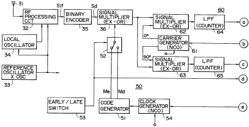
F'ig. ~l. is a b7.ock diagram of a spread spectrum
sigrza.l rece:ivi.ncJ apparatus embodying the present invention.
- 11 -
~~~~9"~
This embodiment represents a receiving apparatus for
use in a global positioning system (GPS).
A satellite signal (spread spectrum signal)
received at an antenna 31 is supplied -to a radio
frequency processing circuit 32. Meanwhile an output
of a reference oscillator 33 consisting of a 18.414 Mhz
quartz oscillator is supplied to a local oscillator 34
which produces a local oscillation output where the
output frequency of the reference oscillator and the
frequency ratio thereof are fixed.
The local oscillation output thus obtained is
supplied to the radio frequency processing circuit 32,
where the satellite signal is converted to a signal of
a first intermediate frequency 19.43'7 MI~?z anel:._then is
further converted to a second intermediate frequency
signal Sif of a second intermediate -frequency 1.023
MIIz by the oscillation output of the re:E'erence oscil-
lator 33.
The second intermediate frequency Sif obtained
from the radio frequency processing circuit 32 is
supplied to a binary encoder 35 and is compa-red with a
predetermined threshold level so as to be changed into
a binary signal.
The binary output Sd of 'the binary encoder 35
_ 12 _
is supplied to a signal multiplier 36 consisting of an
exclusive OR circuit.
In this embodiment also, similarly to the
aforementioned conventional example, the technique of
T-dither tracking is used in an inverse spread demodu-
lacing feedback loop 50, and a costas loop is employed
as a data bit demodulating feedback loop 60. Each of
such two loops is formed into a digital circuit configu-
ration, and control signals for the loops are produced
by means of software in a microcomputer 100.
The inverse spread demodulating feedback loop
50 includes a code generator 51 'for generating pseudo-
random noise codes on the receiver side, wherein an
early code Me and a late code Md having a phase differ-
ence of a 1-chip time are generated. (In the GPS
satellite signal, 50-bps orbit parameter data are
processed by spread spectrum modulation in accordance
with a pseudo-random noise code having a chip speed of
1.023 Mhz and a period of 1 msec.)
The early code Me and 'the late code Md from
-the code generator 31. are supplied to an early/late
code selector 52, which is changed every milliseconel by
a switching signal from an early/late swi~t.ch 53 so that
a composite pseudo-random noise code is obtained from
- 13 -
2fl
the code selector 52. Thereafter the composite pseudo-
random noise code is supplied to a multiplier 36 where
the noise code is multiplied by the binary intermediate
.frequency signaJ_ Sd obtained from -the binary encoder 35.
In this example, a clock generator 54 for
generating a drive clock signal to control the phase
and the frequency (chip speed) of the output code from
the code generator 51 consists of a numerical-controlled
variable frequency oscillator (hereinafter referred to
as NCO). A reference clock signal is supplied from the
reference oscillator 33 to the clock generator 54, which
then produces from the reference clock signal a drive
clock signal for controlling the code generator 51 under
control. of a microcomputer.
In the code generator 51, the phase and the
frequency of the early and late pseudo-random noise codes
are controlled by the clock signal. of the controlled
phase and frequency obtained from the clock generator 54.
Consequently the pseudo-random noise code outputted from
the code generator 51 is so controlled as to coincide
with -the phase and frequency of the 'pseudo-random noise
code included in -the intermediate frequency signal Sd
obtained frorn the binary encoder 45, whereby inverse
spread is performed.
_ 14
The costas feedback loop 60 for demodulating
the data bits comprises a carrier generator 61 consist-
ing of an NCO and a 90° phase shifter, fi_.rst and second
multipliers 62 and 63 each consisting of an exclusive OR
gate, low-pass filters 6~ and 65, and a microcomputer 100
for producing control signals for the carrier generator
61. The carrier generator 61 is supplied with the
reference clock signal from the reference oscillator 33
and generates a carrier signal in response to the refer=
ence clock signal under control of the microcomputer 100.
The microcomputer 100 executes, by the use of_
program software, the individual functions shown as
function blocks in Fig. 1. Now the processing .functions
of the microcomputer 100 will be described in detail
below with reference to the function blocks ::gin Fig. 1.
A multiplying means lOl serves to multiply the counted
Values of the low-pass filters 64 and 65 each consisting
of a counter, thereby producing an output which corre-
sponds to the phase difference between the carrier
component in the received signal and the carrier
obtained from the carrier generator 6l. A loop filter
means 102 forms a signal for control:Ling the carrier
generator. 61 from -the output of the multiplying means
101 and supplies the signal to 'the carrier generator 61.
- 15 -
The above means partially constitute the costas loop 60.
Absolute-value detecting means 103 and 104
respectively de-tact the absolute values of the count
outputs from the low-pass filters 64 and 65, and the
detection outputs are added to each other in an adding
means 105. The adding means :105 produces a signal
indicating the level of correlation between the pseudo-
random noise code from the.code generator 51 and the
pseudo-random noise code in the received signal. With
regard to the outputs of the low-pass filters 64 and 65,
absolute-value detection is performed instead of square-
law detection on the basis of the following reason.
In the conventional analog con stitution of Fig.
9, the outputs of -the low-pass filters 7 and ~ have a
relationship of a cosine wave and a sine wave as repre-
sented by broken lines (a) and (b) respectively in Fig.
2A when the aforementioned correlation is attained
between them. Therefore, if the two outputs are added
to each other after square-law detection, it follows that
a signal of a fixed level can be obtained. In this
embodiment, however, the outputs of the low-pass filters
64 and 65 are binary signals. Accordingly -the correlated
Ou'tpLl'tS Of the low-pass filters 64 and 65 are triangular
waves as represented by solid lines (c) and (d) in F~'ig.
- 16 -
2~~~9~r
2A when the aforementioned correlation is attained
between them. Therefore, if -the outputs of the low-pass
filters 64 arid 65 are added to each other after square- -
law detection as in the )mown example, the level of the
added output fails to be fixed regardless of -the
predetermined correlation as shown in Fig. 2B, and it
becomes impossible to discriminate between attainment
and nonattainment of the. correlation.
In contrast therewith, the added output obtained
after absolute-value detection as in this embodiment has
a fixed level as shown in Fig. 2C, whereby an exact
discrimination is rendered possible as to whether the
proper correction is attained or not.
The output of the adding means 105 is fed to a
switch means 106 and is changed by a switching signal
from the early/late switch 53 in synchronism with the
selector 52, so that the switched output is stored in an
early data holding means 107 or a late data holding
means 108. Substantially the switch means 106 is not
required. In this case, a memory area f_or the early
data and a memory area for the late data a-re seler_ted in
response to -the switching signal from the early/late
switch 53, and such early data and late data are stored
in -the selected regions respectively. The output of -the
- 17 -
early data holding means 107 and that of the late data
holding means 108 are supplied to a subtracting means
109 where a subtraction of the two outputs is executed.
lend the result of such subtraction is supplied to a
loop filter means 110, which then forms a numerical
control signal for controlling the phase of the drive
clock signal outputted from the clock generator 54 for
the code generator 51.
The output of the adding means 105 is supplied
to a search signal generating means 111 while being
supplied also to a sync signal detecting means 112. The
search signal generating means 111 generates a search
signal to perform a search in such a manner as to slide
the output code of the code generator 51 by one period
until the predetermined correlation is attained. The
sync signal detecting means 112 keeps monitoring -the
added output and supplies a switching signal to a switch
means ).13 which alternatively determine a search or a
phase control in accordance with the output of the loop
filter l10 and selects either the output of the search
signal generating means 111 or the output of the loop
filter means 1.10. The output of the switch means 113 is
supplied to the clock generator 54.
~-Tex~eina:f~ter the practical processes of the
- 18 -
microcomputer 100 will be described with reference to
flow charts of Figs. 3 through 7 where reference numerals
of the function means correspond to those used in Fig. 1.
The operation shown in Figs. 3 through 7 is repeated
every millisecond corresponding to the chip speed of the ,
pseudo-random noise code. Therefore the low-pass filters
64 and 65 each having a counter configuration are reset
every millisecond.
Referring first to Fig. 3, I data from the low-
pass filter 64 of a counter constitution is inputted (step
201), ,and its absolute value is calculated (step 202).
Similarly, Q data from the low-pass filter 65 of a counter
constitution is inputted (step 203), and its absolute
value is calculated (step 204).
Subsequently the absolute value of the 1 da-ta-
calculated in step 202 and that of -the Q data calculated
in step 204 are added to each other to obtain a result A
(step 205). And in accordance with -the switching signal
from the early/late switch 53, a decision is made as to
whether the current operation mode is an early mode where
the code generator 51 produces an early code Me (step,
206). Tf -the result of such decisian signifies an early
mode, the addition result A is w.r_itten in the early data
stox-age area of a RAM (step 207) . In case -the r-esult of
_. 1 g
such decision signifies an early mode, the addition
result A is written in the early data storage area of a
RAM (step 207). Tn case the result of the decision
signifies a late mode where the code generator 51
produces a late code Md, -the addition result A is written
in the late data storage area of the RAM (step 208).
Thereafter the operation proceeds to the flow
chart of Fig. 4. The partial procedure shown in Fig..4
corresponds to the operation pe-rformed by the sync
detecting means 112 in Fig. 1. More specifically, first
a decision is made as to whether the addition result A
obtained in step 205 is in excess of a predetermined
threshold level or not (step 211). This decision is
executed to find, with regard to -the feedback loop 50,
whether the predetermined co-rrelation is attained or not
between the pseudo-random noise code of the received
signal and the pseudo-random noise code from the code
generator 51.
If -the result of such decision signifies the
attainment of the predetErmined correlation, -the first
timer S is set to ~~10" (10 msec) (step 212) while the
second timer P is set to "30000" (30 sec) (step 21-3),
and then -the operation proceeds to -the flow chart of: F'ig.
6 for forming a control signal for the Costa s loop 60.
- 20 -
~~~~9~~
In case the result of the decision in step 211
signifies nonattainment of the predetermined correlation,
the set value of the first timer S is increased by "1"
(step 214), and a decision is made as to whether the
value of the first timer S is "0" or not (step 215). If
the result of such decision is negative to signify that
the first timer S is not "0", the operation proceeds to
the flow chart of.Fig. 6.
When the result of the above decision signifies
that the value of the first timer S is not "0", the timer
S is set to "1" (step 216), and a decision is made as to
whether the value.of the second tuner P is "0" or not
(step 217). In case the value of the second timer P is
"0", the operation proceeds to the flow chart of Fig. 5
relative to the search signal generating means ll and the
loop filter means 102 in a search mode. If the value of
the second timer P is not "0", the value is decreased by
"1" (step 218), and then the operation proceeds to the
flow chart of Fig. 7 relative to the loop filter means
110 in the feedback loop 50.
In this case, if the at'tainmen't of the predeter-
mined correlation is once detected (correlation lock) in
'the fs~edbzc:)c loop 50, the first tuner S so functions as
not to determine non-correlation unless the result of the
- 2.1 -
decision in step 211 signifies nonattainment of the
predetermined correlation 10 times repeatedly, i.e., for
msec continuously in the flow chart of Fig. 4.
If the correlation locked state is once
detected in the feedback loop 50, the second -timer P is
maintained in that state for a preset time of, e.g., 30
seconds despite the decision of non-correlation (signify-
ing nonattainment of the predetermined correlation
continuously for 10 msec). In this state, however, there
are executed a control of the output of the carrier
generator 61 by the loop filter 102 in the feedback loop
60 and also a control of the phase and frequency of the
output of the clock generator 54 by the loop filter 110
in the feedback loop 50. In case the predetermined
correlation is not attair_ed even after the lapse of 30
seconds, the operation proceeds to the flow chart of Fig.
5 relative to a search for the correlation.
Once the correlation locked state is detected
in the feedback .Loop 50, the correlation non-locked state
is not determined immediately even though the result of
the decision in step 211 signifies the nonattainment of
the predetermined correlation, and the operation does not:
proceed immed:iatel.y to a correlation search mode despite
determination of the correlation non--lock. Therefore,
- 22 -
even if the correlation non-lock is detected far a
moment in a state where the proper correlationship is
not lost practically, as in a case where any obstacle ,
such as an airplane is temporarily present between the
satellite and the receiving apparatus, the operation is
prohibited from proceeding to -the undermentioned correla-
tion search which requires a relatively long time. z~ue
to such contrivance, the feedback loop 50 i.s not affected
substantially by the presence of any momentary interfer-
ence to the reception, so that it becomes possible to
ensure maintenance of the stable reception.
Now a description will be given on the.flow
chart of rig. 5 relative to the search signal generating
means 110 and the loop filter means 102 in a search
mode.
The search in 'this embodiment is performed in
the (allowing manner. The .received signal converted into
an intermediate frequency signal Sif is within a range of
1.023 MHz ~ 15 kHz. Therefore the predetermined correla-
tion can be attained by searching such range. However,
the band-width of the loop filter means 102 is generally
in a frequency range narrower than such search _range,
i.e., v350 Hz in this example, so that the search for the
-correlation is executable merely within the band-width'
- 23 -
of the loop filter means 102.
In this embodiment, therefore, 'the early and
late codes from the code generator 51 are so controlled
as to slide by one period at the center frequency fc
corresponding tovthe output of -the carrier generator 61.
In case -the predetermined correlation is not attained
by such 1-period slide control, the oscillation center
frequency fc of the carrier generator 61 is shifted by
700 Hz, and the slide control for the code generator 51
is executed again. Such control actions are performed
sequentially in a range of ~15 kHz. In this procedure,
changing the frequency fc by 700 Hz is executed in plus
and mints directions alternately.
In Fig. 5, first the correlation non-locked
state is initialized since the predetermined correlation
is not attained in the feedback loop 50 (step 221).
Subsequently a decision is made as to whether a 1-period
sl.i.de (phase control) of the early and late codes from
the code generator 51 has been completed or not (step
222). For example, a predetermined time of 4 seconds in
this embodiment is required for eXecu tion of a correla-
lion search by outputting the entire 1 period a:E the
pseudo-random noise '.code from 'the code generator. 51.
~fhere.fore the decision regarding completion of 'the
- 24 -
1-period slide is made by monitoring the 4-second
timer .
When the result of the decision in step 222
indicates the lapse of 4 seconds, it signifies non-
attainment of the predetermined correlation by the
1-period search of the output from the code generator
51. Therefore a numerical control signal is formed for
changing the oscillation center frequency fc of the
carrier generator (NCO) in the costas loop by a prede-
termined step width ~f = 700 Hz (step 223). And such
numerical control signal is supplied to the carrier
generator 61 (step 224). Thereafter a numerical control
signal for sliding the output of the code generator 51
again by 1 period is forrned and then is supplied to the
clock generator 54 (step 225).
When the result of the decision in ~>tep 222
indicates no lapse of 4 seconds, it signifies that the
1-period slide of the output of the code generator 51
has not yet been completed. Accordingly the oscillation
center frequency fc of -the carrier generator 61 in the
ros~t:as loop is left unchanged, and the operation proceeds
to .step 2.25 where a numera.cal control sicJnal :for sliding
the output of the code generator 51. by 1. period i.s con-
tinuous:l.y supplied to 'the clack generator 54. After
- 2.5 -
termination of step 225, -the operation returns to step
201 in F'ig. 3. (See Fig. 7)
As a result of the correlation search described
above, a correlation locked state is detected samewhere
with certainty.
Upan detection of attainment of the predeter-
mined correlation in step 211 of Fig. 4, the operation
proceeds to the flow chart of Fig, 6 relative to the
loap filter means 102 for finely cantrolling the carrier
generator 61. The oleration in this flow chart for
controlling -the carrier generator 61 in the correlation
locked state is performed in the following manner.
First, the carrier generator 61 is set to the
oscillation center frequency fc with attainment of the
predetermined correlation. And in accordance- with the
output of the multiplying means 101 which is an error
signal serving as a reference signal. to control the
carrier generator 61, the oscillation frequency of the
carrier generator 61 is lowered by a predetermined
frequency width of 30 Hz for example with respect to the
center frequency fc when the multiplied output is positive
(indicati.ng that the oscillation frequency is deviated
-toward a hicJher side) . To the contrary, when 'the
multipl:Led ou'tpu't is negative (i.ndicat:ing that 'the
- 26 -
oscillation frequency is deviated toward a lower side),
the oscillation frequer_cy of the carrier generator 61
is .raised by a predetermined frequency width of 30 Hz
for example with respect to the center frequency fe.
Such frequency shift is executed per opera-tion ~.n this
flow chart, i.e., every millisecond. The frequency
shift is repeated for a time of, e.g., 50 milliseconds,
and -the number of positive multip_Lied outputs and that
of negative multiplied outputs during 50 milliseconds
are counted and compared with each other. Such operation
may be performed by a single counter.which counts up the
positive outputs or counts down -the negative outputs.
Tf the oscillation center frequency fc of the
carrier generator 61 is locked to the carrier of the
received signal, the counted value during 50 milliseconds
is "0". Meanwhile, when the oscillation center :Frequency
fc is higher than the lock .frequency, the counted value
becomes posi-ti.ve. And when the oscillation center
frequency fc is lower than the lock frequency, the counted
Value becomes negative. Consequently, in case the counted
value during 50 milliseconds is positive, the oscillation
center frequency fc of the carrier generator 61 is shifted
to be lower by a predetermined step width of 1 FIz or so,
and the same operation is performed at the shifted
oscillation center frequency fc. In case the counted
value durixrg 50 milliseconds is negative, the ascillation
center frequency .fc is shifted to be higher by a prede-
termined step width of 1 I~z or so, and the same operation
is performed at the shifted oscillation center frequency
fc. Due to the control deseri.bed above, the oscillation
center frequency fc of -the carrier generator 61 is caused
to exactly follow up the carrier of the received signal.
In the flow chart of Fig. 6, the counted value s
from the low-pass filters 64 and 65 are mutually multiplied,
and a decision is made as to whether the multiplied output
is negative or not (step 231). If the result of such
decision signifies that the output is positive, the count
COSCNT relative to the cos-tas loop is increased by "1"
(step 232), and a numerical control signal is formed for
lowering the oscillation frequency of the carrier
generator 61 by a predetermined frequency width of 30 ~Iz
or so with respect to the center frequency fc at that
instant (step 233). And sLlCh numerical control signal is
supplied to the carrier generator 61 (step 234). If -the
result of the decision in step 231 signifies that the
output is negative, the count COSCIJT is decreased by "1"
(step 235), and a numerical control signal is formed for.
raising the oscillation frequency of the carrier generator
- 28 -
61 by the aforesaid frequency width of 30 Hz caith
respect to the center frequency fc at that instant (step
236). And the numerical control signal thus produced is
supplied to the carrier generator 61 (step 234).
Subsequently the value of the third tinier C
(initial value = 50) is decreased by "1" (step 23'1).
And a decisiom is made as to whether the value of the
third timer C is "0" or not (step 238). If the result
of such decision signifies that the value of the third
timer C is not "0", it indicates that the predetermined
time of 50 milliseconds has not elapsed yet after set -ting
or changing the oscillation center frequency fc. Then
the operation proceeds ~-to the flow chart of F'ig. 7.
In case the result of the decision in step 238
signifies that the value of 'the third timer C is "0°', it
indicates that the time of 50 milliseconds has elapsed
already after setting or changing the oscillation center
frequency fc. Then a decision is made as to whether the
count COSCNT is "0" or not (step 239). And when the
- count COSCNT is "0", the oscillation center frequency fc
is left unchanged, and the operation proceeds to step
244 where -the third timer C is set to its initial value
5O.
Meanwhile, if the count COSCN'.I' is not "0", a
- 29 -
decision is made as to whether the count COSCNT is
positive or not (step 240). When the result of such
decision signifies a positive value, a control signal
for lowering the oscillation center frequency fc of the
carrier generator 61 by 1 ~3z is formed (step 241) and
then is supplied to the carrier generator 61 (step 243).
Thereafter the operation proceeds to step 244
for initializing the third timer C, and further to step
245 where the count COSCNT is set to "0" for execution
of the next counting action for 50 milliseconds. And
the operation proceeds to the flow chart of Fig. 7.
The flow chart of Fig. 7 shows the operation of
the subtracting means 109 and the loop filter means 110.
Irz this example, the code generator 51 is controlled in
the following manner.
The difference DI between the early data EA and
the late data LA outputted from the adding means 105 is
calculated as DI = EA - LA. And when the difference DI
is positive and greater than a predetermined value to
indicate that the early code Me has a higher correlation
level, the control action is so executed as to further
advance the output phase of the code generator 51.
N~eanwhi:l.e, when -the dif:Eerence DI is negative and greater
-than the predetermined value to indicate that the late
-- 30 -
code Md has a higher correlation level, the control
action is so executed as to delay the output of the code
generator 51. If the difference DI is in a predetermined
range with "0" at the center, the current state is
maintained without any change.
In the p-ractical operation of Fig. 7, the
difference DI in this example is represented by the
count PNCNT of the counter concerned with control of the
code generator. 51. The aforesaid predetermined values
are regarded as counts -I-PN and -PN and, as shown in Fig.
8, the count PNCNT is so preset as to become +PN when
greater than the count -t-PN or to become -PN when smaller.
than the count -PN.
In addition to the above control, the chip
speed (frequency) of the output code of -the code generator
51 is checked on the basis of the output.fre~luency of the
carrier generator 61 in the costas loop 60. This check
is performed by utilizing the existence of a predeter-
mined relationship between the frequency of the carrier_
generator 61 and the output frequency of the clock
generator 5~ which serves as a driving circuit for the
code gexierator 57.. More specifical:Ly, the desired
OSCllla-tlOn frequemry o:E the ca.rrier_ generator 61 in
-the costar loop 60 can be calculated when the feedback
-- 31 -
loop 50 is locked. Conversely, if the costas loop 60
is locked, the set frequency pf the code generator 51
can be calculated .from the resolution of the carrier
generator 61 in the costar loop 60. Since the ratio of
such two frequencies is 1 : 1500, it becomes possible to
achieve a high-precision control of the frequency of the
feedback loop 50 with an accuracy enhanced approximately
1500 times.
In the flow chart of Fig. 7, first the differ-
ence between the early data EA and the late data I'A
outputted from the adding means 105 is calculated, and a
decision is made as tp whether the differEnce EA - LA a.s
negative or not (step 251). If the result of such
decision signiFies that the difference is positive, it
indicates -that the correlation level of -the early code
Me is higher, and therefore the count PNCNT is increased
by "1" (step 252). And then a decision is made as to
whether the count PNCNT is equal to the aforesaid prede-
termined value +PN or. not (step 253). And three control
output values X, Y and Z for the clock generator 54 are
prepared in accordance with the results of such
decision.
:Cf the result o:E the deci~;ion in step 25 3
signifies 'that 'the count PNCNT is -+-PN, 'the control
- 32 -
output X is set to a control. value Nowf for maintaining
the current output phase of the code generator 51
unchanged, while the control outpwts X and Z are set to
a control value Fast for -the clock generator 54 -to
advance 'the output phase of the code generator 51 (step
254).
In case the result of the decision in step 253
signifies that the count PNCNT is not equal to PN, it
indicates -PN < PNCNT < +PN. Therefore the control
output X is se-t to a control value Slow for the clock
generator 54 to delay the output phase of the code
generator 51, while the control output Y is set to a
control value Nowf to maintain the current state, and
another control output Z is set to a control value Fast
for the clock generator 54 to advance the output phase
of t:ne code generator 51 (step 255).
When 'the result of the decision in step 251
signifies that the difference DI is negative, the count
PNCNT is decreased by °'1" since the correlation level
of the l ate code Md is higher (step 256). And a decision
is made as to whether the count PNCNT is equal to the
predetermined value -PN (step 257). If the result of
the decision i.n step 257 signifies that the count PNCNT
is equal to -PN, the control ou'tpu'ts X and Y are set to
- 33 -
a control value Slow fo-r the clock generator 54 to
aelay the output phase of the code generator 51, while
another control output X is set to a control value Nowf
for maintainirig the current output phase or the code
generator 51 (step 258) . In case tre result of the
decision in step 257 signifies that the count PNCIQT is
not equal to -PN, it indicates -PN < PNCNT <+PN, so that
the operation proceeds to step 255.
Subsequently the output frequency of -the code
generator 51 in the feedback loop 50 is calculated by
using the output frequency of the carrier generator 61
in the costas loop 60, and a control value for the clock
generator 54 with respect to such calculated output
frequency is preset (step 258). The current control
value for the clock generator 54 relative to the code
generator 51 is compared with the control value thus
preset, and a dP_ClSlOn is made as to whether the differ-
ence therebetween is within a predeterr.;ined range or
no-t (step 260j. If the -result of such decision ,signifies
-that the difference is within the predete-rmined range,
the control value Y is selected for the clock generator
54 (step 261) . Practicall-y, in the case of -PN < PNCNT <
-t-PN, -the current state is ma_inta_i.necl v.~i.-thowt any chancJe.
Meanwhi-:l-a a.n the case of. PNCN'f _ -I-PN, the control value
_ 34 _
Fast is selected for advancing the output phase of the
code generator 51; and in the case of_ PNCNT ----- -PN, the
control value Slow is selected for delaying the output
phase of the code generator 51.
bdhen the result of the decision in step 260
signifies that the aforesaid difference is beyond the
predetermined range, a decision is made as to whether
the frequency deviation is toward a higher side or not
depending on the pasitive or negative of the difference
(step 262). If the result of such decision signifies
that the frequency deviation is toward a higher side,
the aforementioned control output X is selected as the
value for controlling the clock generator 54 (step
263) . Practically, in the case of -PN < PNCNT < -I-PN or
PNCNT = -PDl, the control value Slow is selected for
defying the output phase of the code generator 51.
i~eancahile in the case of PNCNT ~ +PN, the current
output phase of the code generator 51 is maintained
without any change.
If the result of the decision in step 262
signifies that -the frequency deviation is toward a lower
side ,, the control output Z :is selected as -the value for
controlling 'the clock generator. 54 (step 264). And in
the case of -PN < PNCNT < -f-PN or. PNCN'f _ -~-PN, the control
- 35 -
value Fast is selected f.or advancing the output phase
of the code generator 51. Meanwhile in the case of
PNCNT = +PN, the output of 'the code generator 51 is
maintained in the current state.
The operation shown in the flow charts of
Figs. 3 through 7 is repeated every millisecond.
It is t o be understood that the present inven-
tion is not limited to the global positioning system
(GPS) alone arid may .be applied also to any of spread
spectrum signal .receiving apparatus.
It is obvious that modulation of the carrier
is not limited merely to the orthogonal phase modulation
mentioned in the above embodiment, and a variety of
modulation methods can be adopted as well. Furthermore,
the data such as orbit parameters in the above embodiment
need not exactly be superimposed on the carrier, and
transmission of the carrier alone is also employable.
According to -the present invention, as described
hereinabove, a spread spectrum signal. receiving apparatus
can be constituted by the application of digital high-
density integration and software to consequently realize
low production cost, dimensional reduction, low power
r_onsrzmption and h:i.gh dual.it~y.
Further according t o the present invention
- 36 -
2fl~~~~"~
equipped with a feedback loop for attaining a predeter-
mined correlation between the pseudo--random noise code
of a received signal and -the output of a pseudo-random
noise code generator, an intermediate frequency signal
is encoded to be binary and is multiplied by the output
of the pseudo--random noise code generator, whereby a
balanced modulator employed in a conventional apparatus
is no longer required to eventually elimina-to the
necessity of the circuit technique for retaining the
balance of the modulator.
Moreover, the dig ital constitution enables the
use of a numerical controlled oscillator (N'CO) as a
variable frequency oscillator without the need of a
voltage controlled oscillator (VCO) employed customarily
heretofore, whereby a merit is achievable in :nonrequire-
ment of the circuit technique to maintain the linearity
of the voltage controlled oscillator.
In addition, stable reception is ensured
without the necessity of any arxalog circuit technique
due to the digital configuration described, so that
when the present invention is applied -to a multichannel
receiviricJ apparatus, there occurs neither interference
nor var~.ation between the channels. Beside:~> the above,
the parameters determined by the loop filter. are change-
able with :Eacili.ty by the application of software.
- 37 -