Note: Descriptions are shown in the official language in which they were submitted.
WO 91/192?8 PCT/US91102~33
-1-
PERIODIC PULSE DISCRIMINATION SYSTEM
BACKGROUND OF THE INVENTION
1. Field of theInvention
This invention relates generally to electronic
article surveillance systems and, more particularly, to
electronic article surveillance systems of the type 'that
detect a resonant marker or tag that is planed in a
swept frequency electromagnetic field near the eacit to a
protested area. The system detects perturbations or tag
signals that are generated when the frequency of the
swept field passes through the resonant frequency of the
tag to provide an alarm signal. '
2. Descri.Ltion - -of the Prior Art
Swept frequency electronic article surveil-
lance systems are known. One such system is described
in United States Patent No. 4,812,822. One of the prob-
lems that is encountered by electronic article surveil-
lance systems, including the one described in the afore-
mentioned United States Patent No. 4,812,822, is that
2Q the signal produced by the marker or tag is generally
quite small and the systems must work in noisy environ-
ments and be able to discriminate a valid tag signal
from spurious radiations. Such spurious radiations may
take the farm of interfering carriers and resonances
that have the same characteristics as a tag signal but
are caused by building structures or other metallic
structures in the vicinity that have resonance charac-
teristics similar to those of a tag.
dV0 91/19278 PCT/US91/D2833
s-, S,, '-z
'v
In order to provide the required discrimina-
tion between a tag signal and a spurious signal, the
systems according to the prior art utilize relatively
elaborate signal processing techniques including auto-
s correlation and various filtering f.echniques including
synchronous integration, as described in the afore-
mentioned United States Patent No. 4,812,822, to dis-
criminate between a valid tag signal and spurious
signals or to filter out spurious signals. other exam-
pies of attempts to eliminate spurious signals are dis-
closed in United Patent Nos. 4,11.7,466 and 4,168,496.
United States Patent No. 4,117,466 addresses the problem
of filtering out an interfering carrier by detecting the
beat frequency produced by the interfering carrier and
the swept carrier of the system and inhibiting the
alarm. The system disclosed in United States Patent No.
4,168,496 addresses the problem of spurious signals pro-
duced by resonant structures in the area that generate a
signal that looks like a tag signal. In the afare--
mentioned system, the spurious tag-like signal is sam-
pled and stored, and the stored signal is subsequently
subtracted from the received signal to thereby cancel
out the spurious signal from the received signal so that.
it is not detected as a valid tag signal. While the
aforementioned systems do provide a way to distinguish
between spurious and valid tag signals, they are rela-
tively complex and different approaches must be taken to
discriminate against different types of interfering sig-
. pals, such as interfering carriers and resonances.
SUMMARY
It is an object of the present invention to ,
overcome many of the disadvantages of the prior art
systems.
It is yet another object of the present-inven-
tion to provide a system that discriminates between
valid tag signals and spurious signals with~ut utilizing
extensive signal processing.
WO 91/19278 PCf/US91/02833
r
.. 3
It is yet another object of the present inven°
tion to provide an electronic artic7.e surveillance
system that is better able to discriminate between valid
tag signals and spurious signals.
It is yet another object of the present inven-
tion to provide an electronic article surveillance
system~that identifies a spurious signal based on how
rapidly it appears and utilizes gating techniques to
gate out the spurious signal once it has been identi-
fied.
It is yet another object of the present inven-
tion to provide a system that utilizes a common approach
and circuitry to discriminate against different types of
spurious signals including carriers and resonances.
It is another object of the present invention
to provide a system that can discriminate between tag
signals and signals that are generated by other objects,
but have characteristics that are similar to tag
signals.
It is another object of the present invention
to provide an electronic article surveillance system
that monitors the amplitude and frequency characteris-
tics of signals present in the environment and provides
a diagnostic display indicating the characteristics of
the environment.
It is yet another object of the present inven-
tion to provide a swept frequency electronic article
surveillance system wherein the receiver receives
synchronizing information from the swept transmitter
signal to thus eliminate the~need for an interconnecting
synchronizing line.
It is another object of the present invention
to provide an electronic article surveillance system
that utilizes an adaptive threshold whose setting is
based not only on the amplitude of the received inter-
fering signal, but on its synchronocity.
CA 02059665 1999-OS-13
-4-
It is yet another object of the present invention to
provide an electronic article surveillance system wherein the
adaptive threshold circuit is used in conjunction with a
notch circuit wherein the notch circuit notches out
periodically occurring signals thereby permitting the
adaptive threshold to be set at a low level to maintain full
sensitivity without causing false warnings.
In accordance with the present disclosure, a swept
frequency transmitter whose frequency is swept over a range
of frequencies encompassing the resonant frequency of a
resonant tag generates a signal that is applied to a
transmitting antenna located at an exit to a protected area.
A receiving antenna is also located at the exit to the
protected area and is spaced from the transmitting antenna so
that anyone exiting the protected area must pass between the
transmitting and receiving antennas. The receiving antenna is
connected to receiving and processing circuitry that detects
the presence of a tag passing between the receiving and
transmitting antennas.
In accordance with one aspect of this disclosure,
phase shift networks are interposed between the transmitter
and the transmitting antenna and between the receiver and the
receiving antenna to optimize the coupling between the
transmitter and transmitting antenna and the receiver and
receiving antenna and to provide the optimum field
distribution between the transmitting and receiving antennas.
However, it has been found that the coupling networks provide
a variable attenuation to the swept signal as it is swept
over its range of frequencies, thus amplitude modulating the
signal received by the receiver at the transmitter sweep
rate. Thus, by applying the amplitude modulated signal to
synchronization circuitry within the receiver, the receiver
can be synchronized to the sweep frequency of
WO 91/19278 PCT/US91/02833
-5-
the transmitter without the need for interconnecting
lines.
In addition, the detected signal is applied to
an adaptive threshold circuit and pulse detector that
detects the occurrence of a pulse. Each time a pulse is
detected, a processor determines when the next pulse
should be received if the pulse is a 'tag pulse based on
the known sweep frequency of the transmitter. Pulses
received at times other than the predicted time are
ignored. If pulses are repeatedly received at the pre-
dicted time, it is likely that a tag is present;, how-
ever, if the pulses continue to be received for more
than a predetermined time interval, they are likely
caused by a spurious signal, and the threshold of the
adaptive threshold is increased so that the pu;Lses are
ignored. In addition, pulses from the pulse detector
axe applied to a notch pulse generator circuit that
detects recurring pulses at a particular portion of the
swept frequency range and utilizes gating circuitry to
notch out such pulses if they persist for a predeter-
mined time period, thereby effectively patching out
interfering carriers and resanances that persist for
longer time periods than a tag signal would normally
persist. Once an interfering signal has been notched
out, the threshold of the pulse detector circuit is
lowered to maintain system sensitivity even in the pres-
ence of an interfering signal. Subsequent signals are
analyzed, and if a signal that is in synchronism with
the sweep frequency of the transmitter is detected, and
if the amplitude of the detected signals rises and falls
rapidly, such a signal is characteristic of a tag
signal, generated when a tag moves through the protected
zone, and an alarm is sounded. A diagnostic display is
provided so that a person analyzing the performance of
the system and the environment may readily be able to
determining the conditions of the environment in which
the system is located.
CA 02059665 1999-OS-13
-6
In addition, circuitry capable of distinguishing
between a tag and other objects present in the vicinity or
being carried through a protected exit that generate signals
that are similar to tag signals may be provided. A circuit
that disables the system to prevent false alarm in the event
of transmitter failure is also provided.
Embodiments of the invention will now be described
with reference to the accompanying drawings in which;
FIG. 1 is a block diagram of the system embodying the
invention;
FIGS. 2 and 3 are schematic circuit diagrams of the
circuitry shown in block diagram form in FIG. l;
FIGS. 4 and 5 illustrate the waveforms of the signals
present at various points of the circuits of FIGS. 1-3 when a
tag or an interfering signal is detected by the system;
FIGS. 6 and 7 are schematic diagrams showing
alternative ways to discriminate between synchronous and non-
synchronous signals:
FIG. 8 illustrates an alternative embodiment of the
adaptive threshold circuit of FIG. 3;
FIG. 9 is a schematic diagram of a circuit that
discriminates between a real tag and other objects in the
vicinity of the system that generate signals similar to those
generated by a tag: and
FIG. 10 is a circuit diagram of a circuit that
disables the system in the event of a transmitter failure to
prevent the generation of a false alarm.
DETAILED DESCRIPTION OF THE PREFERRED EMBODIMENTS
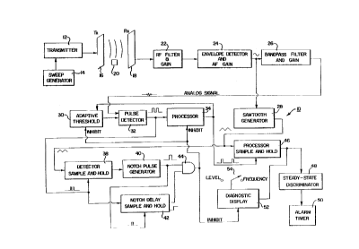
Referring now to the drawings, with particular
attention to FIG. 1, there is shown a block diagram of the
system according to the present invention, generally
designated by the reference numeral 10. The system
WO 91/19278 PCT/US91/02833
~ ~; h
utilizes a transmitter 12 whose transmitting frequency
is swept over a range of frequencies by a sweep genera-
tor~l4. In the illustrated embodiment, the transmitter
is. swept over a range of frequencies.from 7.4 mHz to.8.8
mHz at a sweep rate of 178 Hz, but it. should be under-
stood that other transmitting freguericies and other
sweep frequencies may be used. The output of the trans-
mitter 12 is applied to a transmitting antenna 16 that
is located at an exit to an area protected by the system
10. A receiving antenna 18 is also located at the exit
to the protected area in a spaced relationship from the
transmitting antenna 16 so that a tag, such as a reso-
nant L-C tag 20, or other tag, whether active or pas-
sive, passing between the transmitting antenna 16 and
the receiving antenna 18 will be detected. The output
of the receiving antenna 18 is applied to a receiver
that includes a radio frequency filter and gain circuit
22 that is tuned to the range of frequencies transmitted
by the transmitter 12. The output of the radio fre-
quency filter and gain circuit 22 is connected to an
envelope detector and audio frequency gain circuit 24,
which envelope-detects the output of the radio frequency
filter and gain circuit 22 and amplifies the detected
signal. The output of the envelope detector and audio
frequency gain circuit 24 is applied to two signal pro-
cessing channels: a bandpass filter and gain circuit 26
that provides an analog signal that includes any signal
from the tag 20, and a synchronizing channel that
includes a sawtooth generator 28. The sawtooth genera-
for 28 generates a sawtooth whose amplitude is propor-
tional to the instantaneous frequency of the transmitted
swept frequency signal and is used to synchronize the
receiver signal processing circuitry to the transmitter
sweep frequency.
The bandpass filter and gain circuit 26 has a
pass band centered about 4 kHz and is operative to pass
signal components in the range of frequencies generated
WO 91/19278 P(.'T/US91/02833
4~ ~~ ~. yy .. v.... .
by the tag 20 and to reject other signals, such as the
178 Hz sweep frequency. The output of the bandpass
filter and.gain circuit 26 is applied to a pulse detec-
tor circuit 32 that provides an output pulse whenever
S the signal from the bandpass filter and gain circuit 26
exceeds a predetermined threshold. Z'his threshold is a
DC voltage level that is adjusteautomatically by the
adaptive threshold circuit 30, later described. The
purpose of the adaptive threshold circuit 30 is to in-
crease the detection threshold of the pulse detector 32,
thereby reducing receiver sensitivity in the presence of
environmental noise. In the absence of noise, the
threshold of the adaptive threshold circuit 30 is set
low to optimize system sensitivity.
Z5 The adaptive threshold circuit works in con-
junction with the pulse detector 32 to provide an output
pulse whenever the threshold of the adaptive threshold
circuit 30 is exceeded. The pulse from the pulse detec-
tor 32 is applied to a processor 34. The processor 34 .
operates much like a timer and gate circuit that permits
the passage of a first pulse therethrough, but preuents
the passage of additional pulses for a predetermined
time thereafter. In the present case, the predetermined
time is almost equivalent to the time required for the
sweep generator 14 to complete one full sweep of its
sweep cycle. The reason for this is that if a valid tag
pulse were detected, the next tag pulse whose occurrence
could be predicted would occur one sweep time later.
Thus, if the signal detected were a tag pulse, the next ,
predictable tag pulse would occur one sweep later, and
anything in between (other than the tag pulse on the
return sweep, whose time of occurrence is not pre-
dictable) would be noise or interference and is gated
out. When valid tag pulses are applied to the processor
34, the processor will output a stream of pulses which
WU 91/19278 PCT/US91/02833
'~~~~t;~
vJ ~ ~f
-g-
are very narrow and evenly spaced, since they are syn-
chronized to the transmitter sweep. Noise or interfer-
ence signals are not synchronized to the transmitter
sweep, and therefore consecutive pulses seen at the out-
s put of the processor 34 will vary in pulse width and
timing. The output of the processor 34 is provided to
the adaptive threshold.circuit 30 where the pulses are
' integrated to produce a DC voltage level. This DC volt
age level slowly varies according to how closely the
1p pulses from the pulse detector 30 are synchronized to
the transmitter sweep. The DC voltage from the adaptive
threshold 30 is applied as a reference voltage to the
pulse detector 32. Thus, when detector pulses appear
which are synchronized to the transmitter sweep, the
15 processor 34 provides narrow pulses to the adaptive
threshold circuit 30, which integrates the pulses to
produce a threshold voltage which is gradually increased
until the pulses are not detected, or they appear less
synchronous. The response time of the adaptive thresh-
20 old 30 is slow compared to the pulse amplitude increase
seen at the output of the bandpass filter and gain
stages 26 when a tag moves through the protected zone.
Therefore, a tag signal which is changing in amplitude
will be detected by the pulse detector 32, while a
25 signal which is synchronous but stationary in amplitude
will be rejected. Periodically occurring signals
resulting from interfering sources such as interfering
carriers or from resonant circuits in the vicinity of
the system generally persist for a longer period of time
30 than is required for a tag to pass between the antennas
16 and 18, and consequently, long duration signals are
not considered to be tag signals and the threshold is
raised so that such long duration signals are ignored.
In addition, the output of the pulse detector
35 32 is applied to notch pulse circuitry including a
detector sample and hold circuit 38, a notch pulse
generator 40, a notch delay sample and hold 42 and an
WO 91f19278 PCT/US91/02833
n C"
61 ~ ~. ~'' '4i :.~
-1~-
AND gate 44. The function of the notch generating
circuitry is to identify pulses from the pulse detector
32 that are likely to be caused by interferincJ carriers
or resonances in the area, and to gate them out, for
example, by inhibiting the processor 34, so that they
will not cause an alarm to be generated. The adaptive
threshold circuit 30 will also be disabled, and thus not
desensitize the system once the interference pulses have
been identified and gated off. The output of the pro-
censor 34 is applied to further processing circuitry,
including a processor sample and hold circuit 46 and a
steady state discriminator 48 that further analyzes the
output of the processor 34 for a signal of the type
caused by a tag, namely, a signal that recurs at the
sweep frequency of the sweep frequency generator 14 and
rises quickly as the tag enters the area between the
antennas 16 and 18, persists for a short period of time,
and then decays rapidly as the tag 20 exits the area.
Upan the occurrence of such a signal, the steady state
discriminator 48 will apply a signal to an alarm tier
50 that will trigger an alarm for a predetermined time
period. The operation of the processor sample and hold
circuit 46 and the steady state discriminator 48 will be
discussed in greater detail in conjunction with FIGS. 2
and 3 as will be the operation of the adaptive threshold
circuitry and the notch pulse circuitry.
Tn accordance with another important aspect of
the present invention, a diagnostic display circuit 52
monitors the condition of the processor sample and hold
circuitry 46 to provide an indication to a technician or
installer of the environmental conditions at the instal-
lation site. The diagnostic display can provide in
easily readable form the amplitudes and frequencies of
any interfering signals and indicate whether such
signals are random noise or repetitively occurring
signals such as those produced by interfering carriers
WO 91/19278 PCT/U~91102833
Cl ~~ :u a
-11-
or resonarices. A switch 54 determines whether the diag-
nostic display displays the frequencies or amplitudes of
the-signals in the environment.
Referring now to FIG. 2, the RF filter and
gain circuit 22, the envelope detector and audio
frequency gain circuit 24, the bandpass filter arid gain
26 and the sawtooth generator 28 are shown in greater
detail. As is shown in FIG. 2, the RF filter and gain
circuit 22 is connected to the antenna 18 which in the
illustrated embodiment comprises a pair of antenna loops
18a and 18b by means of a coupling network 100. The
function of the coupling network 100 is to provide
antenna matching and to provide a 90° phase shift
between the loops 18a and 18b which may be, for example,
two loops. of an antenna of the type described in United
States Patent No. 4,872,018. In the illustrated embodi-
ment, the coupling network 100 comprises a pair of
transformers 102 and 104 that provide the desired
impedance matching through the loops 18a and 18b, and a
90° phase shift network comprising resistors 106 and 108
and capacitors 110 and 112. A field effect transistor
114 serves as an RF amplifier, and the output of the
transformer 104 is coupled to the gate of the field
effect transistor 114 by a resistor 116 and a capacitor
118. In the illustrated embodiment, a field effect
transistor is used as the RF amplifier because of its
low noise figure and good intermodulation rejection
characteristics relative to those of a bipolar tran-
sistor. The field effect transistor 114 has a source
resistor 122 and a drain resistor 124 and its drain ter°
urinal is coupled,to the base of a transistor 126 by a
network comprising a coupling resistor 128, a fixed
capacitor 130, a variable capacitor 132, an inductor 134
and a resistor 136. The aforementioned series L-G
coupling network determines the radio frequency to which
the receiver is tuned and is adjustable by means of the
capacitor 132. A resistor 138 serves as a collector
WO 91/19278 PCT/US91l02833
-12-
resistor for the transistor 126 and a pair of resistors
140 and 142 serve as biasing resistors. A transistor
144~is coupled to the collector of 'the transistor 126 by
a resistor 146 and a capacitor 148 and provides addi-
tional radio frequency gain. A resistor 150 serves as a
collector resistor for the transistor 144 and a pair of
resistors 152 and 154 serve as biasing resistors. The
RF filter and gain circuit 22 has an overall phase shift
of approximately 180° to reduce the possibility of
oscillation. Negative feedback is used around the tran-
sistors 140 and 144 to obtain a low input impedance to
reduce the pick up of spurious signals.
The output of the radio frequency filter and
gain circuit 22, taken at the collector of the transis-
for 144, is a radio frequency signal that has a
frequency equal to the instantaneous frequency of the
swept signal transmitted by the transmitter 12 and an
amplitude that has been amplitude modulated by the
coupling network 100 as the transmitter is swept over
its range of frequencies. The coupling network 100 and
a similar network between the transmitter and transmit-
ting antenna attenuate the higher frequencies of the
sweep range. Thus, the received signal is amplitude
modulated at the sweep frequency and has its peaks at
low frequency excursions of the sweep and its valleys at
the high frequency excursions. The modulated envelope
at the output of the transistor 44 is also slightly dis-
torted by the presence of any tag in the vicinity of the
antenna 18 as the transmitter frequency is swept through
the resonant frequency of the tag.
The amplitude modulation of the output signal
from the transistor 144 is recovered by the envelope
detector and gain circuit 24. The output of the tran-
sistor 144 is applied to an envelope detector comprising
a diode 156, a capacitor 158 and a resistor 160 via a
resistor 161. The diode 156 is forward biased so that
the signal applied to the diode 156 need not exceed its
WO 91/19278 PC'I'/US91/02833
>,
-13-
forward diode drop of approximately 0.7 volts before
detection can take place in order to improve sensitivity
of the detector. The signal at the junction of the
diode 156, capacitor 158 and resistor 160 is an audio
frequency signal that is representative of the envelope
of the radio frequency signal at the collector of the
transistor 144. The detected audio signal is coupled
via a coupling capacitor 164 to an amplifier 162 for
amplification thereby. A resistor 3.66 and a Zener diode
l0 168 provide a reference voltage to the amplifier 162 via
a resistor 170. The reference voltage is also applied
to other portions of the circuit. ~. pair of resistors
172 and 174 and a potentiometer 176 form part of a feed-
back loop around the amplifier 162 and are used to con-
trol the gain of the amplifier 162.
The output of the amplifier 162 is connected
to synchronizing circuitry and to signal processing '
circuitry of the receiver. The amplitude modulation
introduced by the antenna coupling network provides syn-
chronizing information to the receiver and the signals
produced by a tag in the vicinity are detected by this
processing circuitry. The synchronizing circuitry
includes a comparator 178 within the sawtooth generator
28 that is connected to the output of the amplifier 162
by a coupling network including a pair of resistors 180
and 182 and a capacitor 184. The coupling network oper-
ates as a differentiating network so that the comparator
178 changes state each time the slope of the signal from
the amplifier 162 'changes direction. Thus, the output
of the comparator 178 changes state each time the swept
RF signal changes direction, i.e., at the peaks and
valleys of the modulation introduced by the antenna
coupling network. Consequently, the output of the
comparator 178 is a square wave which defines the maxi-
mum and minimum frequency excursions of the swept RF
signal.
WO 91/1927$ PCT/US91/02$33
,~ ~~ E=
The output of the comparator 178 is buffered
by a gate 186 and applied to an integrator comprising an
amplifier 188, feedback circuitry including a pair of
capacitors 190 and 192, a pair of rsaistors 194 and 196
and a diode 198. The integrating circuit serves to
integrate a square wave signal from the gate 186 whose
transitions occur at the extreme exs~ursions of the sweep
of the transmitted signal. Consequently, the output of
the amplifier 188 is a triangular wave signal having
peaks and valleys corresponding to 'the extreme excur-
sions of the radio frequency signal and linear slopes
connecting the peaks and valleys. This triangular wave
signal is subsequently used to provide synchronization
for the tag detection circuitry. Although a triangular
or sawtooth wave signal~is particularly convenient for
use in the synchronization circuits because its ampli-
tude is linearly related to the instantaneous frequency
of the transmitter, thus making it relatively easy to
ascertain the instantaneous frequency, a periodic wave-
form having other wave shapes may be used. A pair of
resistors 200 and 202 provide bias for the amplifier
188.
The output of the amplifier 162 also contains
the tag signal when a tag is present in the detection
zone. However, the amplitude of the tag signal is gen-
erally substantially smaller than the amplitude of the
amplitude modulation introduced by the antenna coupling
networks as the transmitter is swept over its frequency
range. However, while the amplitude of the tag signal
is considerably smaller than the amplitude introduced by
the sweep of the transmitter, the frequency components
of the tag signal are considerably different than those
of the sweep frequency. For example, while the sweep
frequency is on the order of 178 Hz, the frequency
camponents of the tag signal are cewtered around
approximately 4 kHz. Consequently, by passing the
WO 91!19278 PCf/1JS91l02833
' .f,. n _
-15-
detected signal from the amplifier 162 through a band-
pass filter centered about 4 kHz, most extraneous
signals, including the sweep signal are substantially
attenuated, and the delectability of the tag signal is
enhanced. The filtering is accomplished by the bandpass
filter and gain circuit 26 that filters out extraneous
components of the detected signal before the detected
signal. is applied to the processing circuitry that
detects the presence of a tag.
In the embodiment illustrated in F'IG. 2, the
bandpass filter is fabricated as a high pass and a low
pass filter connected in tandem. Three amplifiers 204,
206 and 208 and associated compone:zts operate as a low
pass filler that attenuates frequencies below 4 kHz
including the 178 Hz sweep frequency. An amplifier 210
and associated circuitry provide gain to the low pass
filtered signal and three amplifiers 212, 214 and 216
and associated components serve as a high pass filter to
attenuate frequencies above 4 kHz. Thus, the combina-
tion of the high pass and low pass filters serves as a
bandpass filter centered around 4 kHz to permit the
passage of the tag signal and to attenuate other fre-
quencies. Because high pass and low pass filters of the.
type forming the bandpass filler 26 are well known, and
because various types of filters may be used to provide
the desired bandpass filter characteristics, the cir-
cuitry of the bandpass filter and gain circuit 26 will
not be discussed in detail.
Referring now to FIG. 3, the adaptive thresh-
old circuit 30 feeds a comparator 300 that has a thresh-
old that is determined by a pair of resistors 302 and
304 and a variable resistor 306 as well as a feedback
signal received from the processor 34. The feedback
signal from the processor 34 is integrated by the resis-
for 304 and a capacitor 307. The comparator 300
receives the filtered analog signal from the amplifier
216 of the bandpass filter 26 via a resistor 308 and
WO 91/19278 PCT/LJS91/02833
_16_
compares it with the variable threshold signal to
provide an output from the pulse detector 32, which
comprises a comparator 300 and a gate 33 in FIG. 3,
whenever the signal received from the amplifier 216
exceeds the variable threshold. The: output of the gate
33 is applied to the processor 34 which includes a
monostable multivibrator 310 and as~~ociated circuitry
including resistors 312, 314 and 31F>, capacitors 316,
318 and 320 and a variable resistor 322. The variable
resistor 322 cooperates with the resistor 314 and the
capacitor 318 to determine how long the multivibrator
remains triggered following the detection of a pulse by
the pulse detector 32. Typically, the timing is
selected so that once the multivibrator 310 is trig-
gated, it is non-responsive to further signals from the
gate 32~ for a time period corresponding to nearly one
sweep of the sweep frequency generator 14. A monostable
multivibrator suitable for use as the multivibrator 310
is an MC14538B multivibrator manufactured by Motorola,
Inc., but others can be used.
The feedback signal for a variable threshold
circuit is obtained fram the Q output of the multi-
vibrator 310. As long as the multivibrator 310 is not
triggered, the Q output is in its high state, and if,
the multivibrator 310 remains untriggered for a suffi-
ciently long time, the capacitor 307 will charge to a
value determined by the high state value of the Q out-
put divided by the voltage divider action of the resis-
tors 302, 304 and 306. Under these conditions, the
adaptive threshold voltage is close to the analog
voltage received.from the amplifier 216 and maximum
sensitivity to perturbations in the analog signal is
achieved. However, each time the multivibrator 310 is
triggered, the Q output goes low for a period of time
corresponding to approximately one sweep period of the
sweep signal. This results in a reduction in the inte-
grated voltage appearing across the capacitor 307, and
WO 91/19278 PCT/US91/02833
_1~-
moves the threshold voltage away from the analog voltage
thereby desensitizing the system. The more often the
multivibrator 310 is triggered, the more the threshold
voltage is moved away from the analog voltage. This
results in a desensitizing of the system in noisy envi-
ronments to a point where the threshold is moved away
from the analog signal by an amount sufficient to pre-
vent the peaks of the analog signal from crossing the
threshold which reduces the possibility of a false alarm
being generated by a spurious signal.
The output of the processor 34 is coupled to
the processor sample and hold circuit 36 that includes a
sampling gate 324 that samples the sawtooth signal from
the amplifier 188 (FIG. 2) whenever the Q output from
Z5 the multivibrator 310 is high and applies the sampled
signal to a capacitor 326. A circuit suitable for use
as the sampling gate 324 and other sampling gates used
in the illustrated embodiment is a type MC14066B analog
switch manufactured by Motorola, Inc., but others may be
used. The sampled signal on the capacitor 326 is
applied to a buffer 328 prior to application to the
steady state discriminator 48. The signal from the
multivibrator 310 is also divided down by a pair of
resistors 330 and 332 and filtered by a capacitor 334 to
provide a signal usable by a diagnostic display circuit
that will be discussed in a subsequent portion of the
application.
The steady state discriminator 48 includes a
comparator 336, a pair of resistors 338 and 340, a pair
of capacitors 342 and 344 and a pair of diodes 346 and
348. The purpose.of the steady state discriminator 48
is to detect a lack of changing conditions at the output
of the buffer 328. The lack of a changing condition at
the output of the buffer 328 indicates that a syn-
chronous signal such as a tag signal is being detected
and is indicative of an alarm condition. When the out-
put from the.buffer 328 is a steady state output, the
WO 91/19278 PCT/U591/02833
~~lg~~y -18-
comparator 336 is biased effectively by a voltage
divider formed by the resistor 338, the diodes 346 and
348 and the resistor 340. Under these conditions, the
voltage applied to the negative input of the comparator
336 is above the voltage applied to the positive input
and the amplifier is in its cut-off (low) state. How-
ever, if the output of the buffer 328 contains fluctua-
tions, those fluctuations are rectified by the diodes
346 and '348. Such fluctuations result from the sampling
gate 324 causing the voltage on capacitor 326 to follow
the triangle waveform at the output of amplifier 188 for
a relatively wide portion of the sweep period. This
causes the capacitor 342 to be negatively charged and
the capacitor 344 to be positively charged thereby mak-
ing the positive input to the comparator 336 positive
with respect to the negative input and causing the com-
parator 336 output to be in the high state. Thus, the
low-going output of the comparator 336 is indicative of
the detection of a tag.
The output of the steady state discriminator
48 is applied to the alarm timer 50 that comprises a
monostable multivibrator 350 and a transistor 352 and
associated circuitry that are triggered by the compara-
for 336 when the output of the comparator 336 is indica-
five of the presence of a steady state condition at the
output of the processor sample and hold 46 and, particu-
larly the output of the buffer 328. The monostable
multivibrator 350 together with its associated compo-
nents operates as a timer that energizes the transistor
352 and causes the transistor 352 to energize an annun-
ciator such as a beeper, siren or a horn 354 for a pre- .
determined amount of time. A circuit comprising a
capacitar 349, resistors 351 and 355 and a diode 353
determine the length of time that the alarm is sounded.
A circuit including a capacitor 357, a resistor 359 and
a diode 361 inhibits the multivibrator 350~when power is
initially applied to the system to prevent an alarm from
WO 91/19278 PCT/US91/02833
r
-19-
being generated during power up or during a power drop
out. Inasmuch as any suitable timer may be used as the
timer 50, the specific details of the circuitry of the
timer 50 will not be discussed.
The output of the pulse detector 32 controls
the operation of the detector sample and hold circuit 38
which includes a sampling gate 356, a resistor 358 and a
capacitor 360. The sawtooth waveform from the amplifier
188 is applied to the sampling gate 356 via the resistor
358 and the sawtaoth waveform is sampled and applied to
the capacitor 360 for as long as the pulse detector 32
provides a high state signal indicating that a pulse is
present, i.e., that the analog signal has exceeded. the
threshold voltage. Thus, the capacitor 360 charcJes to a
15' voltage that corresponds to points on the sawtooth wave-
form that are indicative of the frequency of a distur-
bance signal. The notch pulse generator circuit 40
consists of comparators 362 and 364, AND gate 3?4 and a
resistive divider network described hereinafter. The
output of the sampling gate 356 is applied to the nega-
tive input of a comparator 362 and to the positive input
of a comparator 364. Comparators 362 and 364 form a
"window" comparator in conjunction with AND gate 374,
with an upper and lower voltage threshold. The output
of gate 374 will be high whenever the voltage on capaci-
tor 360 is between these two thresholds, as next
described. Comparators 362 and 364 receive the sawtooth
signal from the amplifier 188 via a resistive divider
network comprising resistors 366, 368, 370 and 372. The
function of the resistive divider is to provide a DC
offset to the sawtooth waveform so that the sawtooth
waveform appearing at the junction of the resistors 366
and 368 and applied to the positive input of the com-
garator 362 has a positive offset with respect to the
sawtooth waveform appearing at the junction of the
resistors 370 and 372 and applied to the negative input
of comparator 364. Thus, when the sampled voltage on
W~ 91/19278 PCT/US91/02833
.
-20-
J
the capacitor 360 is below the sawtooth voltage appear'
ing at the junction of the resistors 366 and 368, the
comparator 362 will provide a high state output. Simi-
larly, when the voltage across the capacitor 360 is
above the sawtooth voltage appearing at the junction of
the resistors 370 and 372, the comparator 364 will pro-
vide a high state output. The outputs of the compara-
tors 362 and 364 are applied to an R,idD gate 374 which
provides a high state output only when the inputs from
the comparators 362 and 364 applied thereto are both
high. This condition only occurs when the amplitude of
the voltage across the capacitor 360 is greater than the
amplitude of the sawtooth voltage appearing at the junc-
tion of the resistors 370 and 372 and below the voltage
of the waveform appearing at the junction of the resis-
tors 366 and 368. The output pulse Pram the gate 374 is
referred to as a notch pulse and will be described in
greater detail in a subsequent portion of the applica-
tion. It should be noted that resistor 358 and capaci-
for 360 form a slow integrator so that extraneous noise
pulses do not pull the notch pulse away from a steady
interference signal.
The outgut of the notch pulse generator 40 ,
(gate 374) controls the operation of another sampling
gate 376. Within the notch delay circuit 42, the gate
376 samples the analog signal from the amplifier 216 of
the bandpass filter and gain circuit 26. The output of ,
the sampling gate 376 is applied to a capacitor 378 via
a diode 380 and a resistive dividing network comprising
a pair of resistors 382 and 384. The sampling gate 376
samples the analog voltage from the amplifier 216 when- .
ever a notch pulse is received from the gate 374 and
applies the.sampled voltage to the capacitor 378 via the
diode 380 and the resistors 382 and 384. The sampled
voltage appearing across the capacitor 378 is applied to
a comparator 386 that provides a high state output when
WO 91/19278 PCT/U991/02833
ever the sampled voltage exceeds a fixed reference volt-
age, such as the fixed valtage appearing across'the
Zener diode 168 (FIG. 2). The output:. of the comparator
386 is applied to a slow attack, fast decay circuit com-
prising a capacitor 388, a pair of resistors 390 and 392
and a diode 394. The slow attack, fast decay circuit
serves to charge the capacitor 388 slowly through the
resistor 390 when the output of the camparator 386 goes
from its low state to its high state, and to discharge
l0 the capacitor 388 rapidly through the diode 394 and the
resistor 392, and also the resistor 390 when the output
of the comparator 386 goes from its high state to its
low state.
The notch pulse generator 40 provides two
notch pulses during each sweep period and the notch
pulse delay samples and integrates the analog signal and
provides a high state output when the integrated analog
signal exceeds the reference voltage. The output pulses
from the notch pulse generator 40 are applied to the AND
gate 44 as is the output of the notch delay circuit 42.
Thus, the output of the AND gate 44 goes high each time
a notch pulse is generated by the notch pulse generator
40 provided that the voltage across the capacitor 388 of
the slow attack, fast decay network of the notch delay
42 is also high. Thus, a notch pulse is generated at
the output of the gate 44 which is coincident in time
with the passage of the transmitter sweep through a fre-
quency at which an interference signal persists for a
sufficiently long time interval defined by the notch
pulse delay circuit 42. The notch pulses from the AND
gate 44 are applied to the multivibrator 310 via a diode
396 and serve to inhibit the triggering of the multi-
vibrator 310 during the duration of a notch pulse.
Thus, when notch pulses are present, the pulses from the
pulse detector 32 are inhibited from triggering the
multivibrator 310. Consequently, the "notched out
pulses" are not transmitted to the processor sample and
WO 91/19278 PCT>tJS91/02833
:.%
~''U -22-
hold 46 and consequently, cannot generate an alarm. In
addition, since the "notched out" pulses do not trigger
the multivibrator 310, they have no effect on the
output of the multivibrator 310, and hence do not alter
the adaptive threshold signal 30. ~~s a result, once
pulses resulting from an extraneous carrier or a struc-
tural resonance'have bean "notched out'°, the adaptive
threshold is again moved close to the amplitude of the
analog signal, and full sensitivity to true tag signals
is maintained at frequencies other than those blanked by
the notch even in the presence of an interfering carrier
or structural resonance. The detector sample and hold
38, the notch pulse generator 40 and the notch delay
sample and hold 42 work together to (1) identify that a
signal is present, (2) seek out the frequency of the
signal and (3) determine if it is an unwanted signal
based on its duration and, if so, inhibit detection of
signals at that frequency, for as long as they persist.
When installing and servicing electronic
article surveillance systems, it is desirable to provide
the installer or service person information regarding
the environment in which the system is installed. In
particular, it is desirable to provide the installer
with information relating to the frequency of any inter-
fering carrier or structural resonance and how likely
such interference signals are to cause the system to
false alarm, based on the relative noise level. Thus,
in accordance with another important aspect of the pre-
sent invention, there is provided a diagnostic display
system generally designated by the reference numeral
400. The diagnostic display 400 comprises a light emit-
ting diode bar graph display 402 that is driven by a
display driver circuit 404. A type LNt3916 A/D display
driver circuit manufactured by National Semiconductor
may be used as the display driver circuit 402. The bar
graph display 402 and the driver 404 are responsive to
the amplitude of an analog signal applied to the driver
WO 91!19278 PC.'f/iJS91/02833
_23_ ~~~~~~aC?
404 to provide a display on the bar graph 402 that is
proportional to the amplitude of the analog voltage
applied. The display 400 is disabled by notch pulses
provided to the driver 404 from the gate 44 via a resis-
for 406 and a buffer comprising a transistor 408 and
resistors 41o and 412. Thus, a portion of the display
400 is blanked out during the occurrence of a notch
pulse.
The level or the frequency of an interfering
signal may be ascertained by monitoring either the pro-
cessor 34 or the processor sample and hold circuit 46.
A switch 414 that has an armature 416 that is movable
between an amplitude monitoring pole 418 and a frequency
monitoring pole 420 is used to determine whether ampli-
tude or frequency is to be monitored. Tn the amplitude
monitoring position, the armature 416 is connected to
the amplitude monitoring pole 418 which serves to moni-
tor the Q output of the multivibrator 310 which has
been scaled by the resistors 330 and 332 and integrated
by the capacitor 334. Since the voltage across the.
capacitor 334 is proportional to an average value of the
Q output of the multivibrator (as is the voltage
across the capacitor 307 of the variable threshold
circuit), the voltage across the capacitor 334 is pro-
portional to the variable threshold voltage and is
indicative of the magnitude of any synchronously occur-
ring pulses detected by the system. This voltacJe is
applied to the driver 404 and serves to illuminate the
bar graph 402 in proportion to the magnitude of the
adaptive threshold signal, thus providing an indication
of how synchronous an interfering signal or noise is
with the transmitter sweep rate. Thus, the installer
can quickly assess the likelihood of false alarms based
on the level of synchronous noise displayed on :LED bar
graph 402.
In the frequency mode of display of the diag-
nostic display 400, the armature 416 of the switch 414
WO 9l/19278 PCT/US91/02833
r~ ~ ~=:,
~ , h ~ .r-''.,: :r
-24-
is connected to the pole 420 to monitor the output of
the buffer 328 of the processor sample and hold circuit
46.~ When no synchronously detected signal is present,
the output of the buffer 328 follows the sawtooth wave-
s form and, consequently, the light emitting diodes of LED
bar graph 402 are sequentially illuminated as the
sampled sawtooth signal moves up and down in amplitude.
This gives an illusion that all of the light emitting
diodes of the bar graph 402 are simultaneously lighted.
However, when a steady state condition indicative of a
tag or other pseudo-synchronous or synchronous signal
such as a carrier or resonance is present, the voltage
at the output of the buffer 328 is equal to a voltage
within the sweep range of the sawtooth signal that is
15~ indicative of the particular frequency of the detected
signal. When this signal is applied to the diagnostic
display 400, one or more segments of the bar graph dis-
play is illuminated which approximately corresponds to a
voltage point on the triangle waveform, and relates to
the frequency band within the transmitter sweep range
where the synchronous signal occurs. However, when the
synchronous signal is notched out by the system, the
notch pulse disables the segments of the display 400
that correspond to the frequency band of the notched out
signal. Thus, the light emitting diodes corresponding .
to the notched out~frequency will not be illuminated and
be illustrative of the frequency of the interfering
signal.
The appearance of the bar graph display is
useful in providing information to the installer or ser-
vice person about the environment in which the system is
installed. For example, since the display provides a
display of the synchronocity of signals in the environ-
ment, flickering of a large number of segments provides
'an indication of the presence of random noise. The
flickering of two adjacent segments illustrates the
presence of an interfering carrier. The illumination of
WO 91/19278 PCf/US91/02833
~ ~~ h ~ , i
_25°
a single segment illustrates the presence of a struc-
tural resonance, and the illumination of multiple spaced
single elements illustrates the presence of multiple
resonances. Thus, the display serves as an important
diagnostic tool.
The system is also provided with an indicator
to provide an indication to the user that an interfering
signal such as a carrier or structural resonance that
has a large enough magnitude and has persisted for a
sufficiently long time period to have been notched out
is present. This function is provided by a driver 420
and an indicator light 422 which may contain a light
emitting diode 424. The driver 420 monitors the output
of the notch delay sample and hold circuit that is
agplied to the gate 44, and energizes the indicator
light 422 when the gate 44 is enabled. Thus, the indi-
cator light 422 provides an indication to the user that
interference of sufficient magnitude and duration to
activate the notch circuitry is present to warn him of
potential interference problems.
The operation of the circuit according to the
invention can be better understood by studying the
signal waveforms at various points on the circuit dia-
grams of FIGS. 2 and 3. Referring now to FIG. 4, there
is shown a series of waveforms that illustrate the
detection of a tag. FIGS. 4A-4D illustrate how synchro-
ni2ing information for the system is obtained. FIG. 4A
represents the range of frequencies of the swept fre-
quency signal generated by the transmitter 12 and
applied to the transmitting antenna 16. The swept fre-
quency signal illustrated in FIG. 4A is swept over a
range of, frequencies between 7.4 mHz and 8.8 mHz. FIG.
4B illustrates the output of the envelope detector and
gain circuit 24, more specifically, the signal present
at the output of the amplifier 162 of FIG. 2. The wave-
form of FIG. 48 is essentially a sine wave having its
WO 91/19278 PCf/US91/02833
's i,~ ''2
~u .e; .~ - 2 6
peaks at 8.8 mHz and its valleys at 7.4 mHz. As pre-
viously stated, the sine wave is introduced by the
antenna matching networks in the transmitter and re-
ceiver that attenuate high frequencie:a more than low
frequencies and thus serve to amplituc9e modulate the
envelope of the received radio frequency signal at the
sweep rate. FIG. 4B shows the demodulated envelope.
Although the amplitude of the modulated radio frequency
signal is larger at low frequencies than at high fre-
quencies, because of the polarity of the diode 156, the
demodulated signal of FIG. 4B has a higher amplitude at ,
high frequencies than at low frequencies. Also, a tag
signal is not readily apparent in the waveform of FIG.
~B because the amplitude modulation introduced by the
antenna matching networks is substantially larger than
the tag signal.
The waveform of FIG. 4B provides an indication
of the high and low limits of the sweep and may be used
to synchronize the system, as could any periodic wave-
form having the correct periodicity.. However, it is
desirable to have a waveform that varies linearly
between the limits of the sweep so that an indication of
the instantaneous frequency of the swept signal between
limits may be readily ascertained. In the present .
embodiment, such a linear or sawtooth waveform is gener-
ated in two steps. First, a square wave, as illustrated
in FIG. 4C, is generated by the comparator 1?8 and gate
186 which, because of the differentiating action of the
capacitor 184, generate a transition each time the slope
of the waveform of FIG. 4B changes. When the slope of
the waveform of FIG. 4B goes from a negative slope to a
positive slope, the waveform of FIG. 4C switches from a
low state to a high state, and when the slope of the
waveform of FIG. ~1B goes from a positive to a negative
slope, the waveform of.FIG. 4C goes from a high state to
a low state. The waveform of FIG. 4C is then integrated
WO 91/19278 P~C'f/US91102833
w ~ f' H
C~ P'r ~'l;
-27-
by the integrator including the amplifier 188 and asso-
ciated components to provide the triangular waveform of
FIG. 4D. The triangular waveform of FIG. 4D is sampled
by the various sample and hold circuits such as the
detector sample and hold circuit 38 and the processor
sample and hold circuit 46 of the system to provide
information relating to the synchronism and frequencies
of signals detected by the system.
FIGS.-4E through 4J illustrate the operation
of the tag signal processing channel. The waveform of
FIG. 4E illustrates the magnitude of the analog signal
from the bandpass filter and gain circuit 26 relative to
tze magnitude of the adaptive threshold of the adaptive
threshold circuit 30. The analog signal is illustrated
as a solid line 510 and the position of the adaptive
threshold is illustrated by a dashed line 512» The ana-
log signal 510 has been filtered by the bandpass cir-
cuitry contained in the bandpass filter and gain circuit
26 to remove frequencies outside the band of frequencies
generated by a tag. Consequently, the sinusoidal compo-
nent at the sweep frequency (FIG. 4B) has been removed
and the tag signals are now more readily apparent, as
are signals other than tag signals that fall within the
pass band of the bandpass filter and gain circuit 26.
FIG. 4E illustrates the detected analog signal
produced by a tag as it enters the interrogation field
between the antennas 16 and 18. A tag signal is pro-
duced each time the instantaneous frequency of the
transmitted swept signal coincides with the resonant
frequency of the tag. This occurs twice during each.
sweep cycle, once during the increasing frequency sweep
and once during the decreasing frequency sweep. As is
illustrated in FIG. 4E, the resonant tag entering the
field has a resonant frequency of approximately 8.1 mHz,
about midway between the extremes of the excursions of
WO 91/19278 PCT/US91/02833
~~~~~'~t:.~u
A
-28-
the sweep between 7.4 mHz and 8.8 mHz. As is illus-
trated in FIG. 4E, the tag produces two tag signals dur-
ing each sweep, a tag signal 514 that occurs during the
decreasing frequency portion of the sweep and a tag
signal 516 that occurs during each increasing frequency
portion of the sweep. In addition, the wavefartn of FIG.
4E contains a noise signal 518 that occurred before the
tag entered the interrogation field and was not produced
by the tag. The noise signal 518 will be used to illus-
trate how the system discriminates between noise signals
and valid tag signals.
The pulse detector 32 monitors the waveform
510 and provides an output each time the signal 510
exceeds the threshold 512. The output of the pulse
detector 32 is illustrated in FIG. 4F. As is apparent
' from FIG. 4F, both the noise burst and the tag signals
cause a detector output pulse to be generated. The
noise burst 518 causes a detector output pulse 520 to be
generated when its amplitude exceeds the threshold 512.
Similarly, the tag signals 514 generate output pulses
522 when the threshold 512 is exceeded, and the tag
pulses 516 generate detector output pulses 524 when the
threshold is exceeded.
One of the characteristics of a valid tag
~25 signal is that it is in phase and frequency synchronism
with the sweep frequency of the transmitter. Thus, if a
valid tag pulse is detected during one sweep cycle, the
next tag pulse whose occurrence can be easily predicted
must occur at the same point during the next sweep
cycle, and any signals occurring at other points of the
sweep cycle may be ignored. The prediction of the time
of occurrence of the next valid tag pulse during the
next sweep is accomplished by the processor 34 which
includes a timer that utilizes the multivibrator 310 to
render the system non-responsive to signals occurring in
less than one sweep period following the detection of a
WO 91!19278 PCT/US91/02833
~~ ,'J ~ ~ i
.a ..~
pulse. The output of the processor 34, and more partic-
ularly the Q output of the multivibrator 310 (FIG. 3),
is illustrated in FIG. 4G. In the absence of a detected
signal, the Q output of the multivibrator 310 is high
until a detected pulse is received. As is illustrated
in FIG. 4, when the pulse 520 is generated (FIG. 4F),
the Q output of the multivibrator 310 goes from its
high state 526 to its low state 528. The timing is set
so that the output remains in its low state 528 for a
time period slightly shorter than the sweep period, for
example, for a time period equal to approximately 93-99~
of the sweep time. During the time that the output of
the multivibrator 310 remains in its low state 528, the
multivibrator 310 cannot be retriggered and, conse-
. quently, any pulses detected during that time interval
will be ignored by the system. Once the multivibrator
has timed out, 'the Q output returns to its high state,
as illustrated by a portion 530 of the wavefazzn, until
it is retriggered by the next received pulse.
The pulse 518 that caused the output of the
processor 34 to go from its high state 526 to its low
state 528 was not a valid tag pulse. Consequently,.when
the output of the processor 34 returned to its high
state at point 530, no pulse occurred immediately fol-
lowing the transition to the high state 530 as would
have been the case if the pulse 520 were a detected tag
pulse. Thus, the Q output of the multivibrator 310
remained in its high state 530 until the occurrence of
the next pulse 522, which is a valid tag pulse. Upon
the occurrence of the trailing edge of pulse 522, the
Q output of the multivibrator 310 changes to its how
state for a time period 532 that is slightly shorter
than the sweep time of the transmitter sweep frequency.
After the multivibrator times out, it again returns to
its high state at a point 534. However, another tag
pulse 522 is almost immediately detected, and the Q
output is again returned to its low state for a time
WO 91!19278 PCT/US91/02833
-30-
interval 536. After the time interval 536, the mufti- -
vibrator times out, but is immediately retriggered by
another pulse 522 and the cycle is repeated as long as
the tag is present to provide a series of narrow pulses
534 that are separated by a series of time intervals 536
that axe on the order of one sweep period long or until
the notch circuitry (38, 40, 42) is engaged to inhibit
the triggering of the processor 34, or. until the adap-
tive threshold 30 has had time to increase the detection
threshold voltage of the pulse detector 32 beyond the
level of continuous pulse detection. Any signals occur-
ring during the time periods 536 are ignored and the
pulses 534 are synchronized to the pulses 522, and con-
sequently to the sweep frequency of the transmitter.
The processor sample and hold circuit 46
samples the output of the sawtooth generator 28 under
the control of control pulses from the processor 34.
The output of the processor sample and hold circuit 46,
more particularly the output of the buffer 328 (FIG. 3),
is shown in FIG. 4H. As long as the Q output of the
multivibrator 310 is high, the sampling gate 324 will be
closed (shorted) and the output of the processor sample
and hold circuit 46 will follow the sawtooth waveform .
from the sawtooth generator 28 (FIG. 5D). Thus, when
the Q output of the multivibrator 310 is high, such as
during the time interval 526 (FIG. 4G), the output of
the processor sample and hold 46 will be a replica of
the sawtooth sweep as illustrated by the waveform 536
(FIG. 4H). When the Q output goes low, as during the
low state time interval 528, the processor sample and
hold circuit 46 samples and holds the instantaneous
value of the sawtooth sweep that was present when the
transition to the low state 528 was made, as is illus-
trated by the area 538. When the Q output reverts to
its high state 530, the processor sample and hold output
again follows the sawtooth waveform as illustrated at
540.
WO 91/19278 PC'f/US91/02833
N ~
As long as no valid tag signal is present, the
g output of the multivibrator 310 remains high for
relatively long time intervals. During these time
intervals, the output of the processor sample and hold
circuit 46 follows the sawtooth waveform. Consequently,
the output of the processor sample and hold circuit 46
has relatively large excursions where no valid tag signal
is present. However, once a valid t:ag signal leas been
detected, the g output of the multivibrator remains
high for only relatively short intervals of time which
are synchronized to the transmitter sweep period, for
example, during the time intervals 534 because it is
being constantly retriggered by tag pulses. During most
of the time, the Q output will be at its low state as
illustrated by the areas 536. During these 'times, the
output of the processor sample and hold circuit will
remain relatively constant as illustrated by the areas
542 (FIG. 4H). Only slight perturbations 544 will occur
in the output of the processor sample and hold circuit.
during the time intervals of the pulses 534 (FIG. 4G).
Consequently, when a phase synchronous signal, such as a
tag signal, is being detected, the output of the pro-
cessor sample and hold circuit will remain relatively
constant, thus providing a detectable indication that a
tag has been detected.
The output from the processor sample and hold
circuit 46 is applied to the steady state discriminator
to determine whether a steady state condition indicative
of the presence of a tag exists. The signal from the
buffer 328 (FIG. 3) of the processor sample and hold
circuit 46 is applied to the rectifier circuit compris-
ing diodes the 346 and 348, the resistors 338 and 340,
and the capacitors 342 and 344. As long as no tag is
present, and the output signal from the buffer 328
swings appreciably, the signal from the buffer 328 will
WO 91/19278 PCf/LJS91/U2833
,, r ~, ~', ''< : a.
s~.i~r,;,., .. _ -32-
be rectified by the diodes 346 and 348 so that the nega-
tive input to the comparator 336 will be negative rela-
tive to the positive input, thus causing the output of
the comparator 336 to be high 552. If the output of the
processor sample and hold circuit 46 remains in a rela-
tively steady state, very little AC signal will be
available for rectification by the diodes 346 and 348 in
the steady state discriminator 48. ronseduently, the
polarity of the signals applied to the comparator 336
will be reversed by the voltage divider action of the
resistors 338 and 340 and the diodes 346 and 348, with
the signal applied to the negative input of the compara-
tor 336 being positive relative to the signal applied to
the positive input. When the polarity reversal occurs,
the output of the comparator 336 will change state to a
low state 554.
The operation of the steady state discrimina-
for 48 is illustrated in FIG. 4I. FIG. 4I illustrates
the magnitude of a voltage 546 applied to the positive
input of the comparator 336 relative to the amplitude of
a voltage 548 applied to the negative input of the com-
parator 336 in the presence of the signal from the pro-
cessor sample and hold circuit 46 illustrated in FIG.
4H. When the signal from the processor sample and hold
circuit 46 has relatively large excursions, as is illus-
trated in the region between 536 and 538, the voltage
546 remains above the voltage 548. When the output from
the processor sample and hold circuit 46 is relatively
quiescent, as is illustrated in area 538, the valtages
546 and 548 tend to converge as capacitors 342 and 344
begin to discharge. If the output from the processor
sample and hold circuit 46 remains quiescent far a long
period of the time, as is illustrated by the region 542,
the voltages 546 and 548 will converge until they cross
over at a point 550 where the voltage 548 exceeds the
voltage 546. When the cross-over occurs, the output of
the comparator 336 (FIG. 4J) changes state from a high
WO 91/19278 PCT/US91/02833
~~'~~:,~~~~'h
fd l :.~ :1 '~ r
-33-
state 552 to a low state 554 to indicate that a tag has
been detected and to actuate the alarm.
Referring now to FIG. 5, waveforms that occur
at various points in the system when an interfering
carrier is detected are shown. Also illustrated is how
an interfering carrier or structural resonance is
notched out if it has persisted for a sufficiently long
period of time. FIG. 5A is similar i:o FIG. 4A and shows
the sweep range of the transmitter frequency and is
illustrated to provide a frequency reference for the
other waveforms of FIG. 5. FIG. 5B is the same as FIG.
4C and illustrates the sawtooth output of the amplifier
I88 of FIG. 2. FIG. 5C illustrates the analog signal
resulting from an interfering carrier that appears at
the output of the bandpass filter and gain circuit 26,
specifically at the output of the amplifier 216 (FIG.
2). As is illustrated in FIG. 5C, an interfering
carrier appears at about 7.7 mHz and appears twice per
sweep. The perturbations caused by the interference in
the detected output during increasing frequency sweeps
.are designated by the reference numeral 614 and the per-
turbations caused during decreasing frequency sweeps are
designated. as 616. The pulse detector 32 compares the
analog signal 610 with the adaptive threshold 612 and
provides an output.when the analog signal 610 exceeds
the threshold 612. The output signals from the pulse
detector 32 are illustrated in FIG. 5D. As is illus-
trated in FIG. 5D,~whenever the negative going portion
of analog signal 610 exceeds the threshold 612, an out-
put pulse 622 is generated.
The pulses 622 and 624 from the pulse detector
32 control the detector sample and hold circuit 38 which
samples the sawtooth waveform from the amplifier 188
each time a pulse is generated by the pulse detector 32.
The samples of the sawtooth waveform are illustrated by
a series of circles 626 in FIG. 5E that appear at the
output of the sampling gate 356 and are integrated by
~'O 91/19278 PCTlU~91/02833
~.~t'rf'
c~ ;~ ,. , ~-,. , :r
~.r~~ .~ L _ _34_
the resistor 358 and the capacitor 360 to provide a
voltage 628 on capacitor 3,60 that charges to the average
value of the samples 626. The voltage 628 is compared
with a pair of sawtooth waveforms 6:30 and 632 that are
offset from the sawtooth waveform o:E FIG. 5B by the
voltage divider action of a voltage divider comprising
the resistors 366, 368, 370 and 372. The voltage at the
junction of the resistors 366 and 368 illustrated by the
waveform 630 is applied to the positive input of the
comparator 362 of the notch pulse generator 40 and the
voltage at the junction of resistors 370 and 372 is
applied to the negative input of the comparator 364.
The sampled integrated voltage from the sampling gate
356 is applied to the negative input of the comparator
15. 362 and to the positive input of the comparator 364.
The outputs of the comparators 362 and 364 are applied
to the AND gate 374 which provides a positive output
whenever both of its inputs are positive. The only cir-
cumstances under which both inputs to the AND gate 374
are high is when the amplitude of the voltage 628 is
between the amplitude of the sawtooth voltages 630 and
632.
The output of the notch pulse generator 40,
more particularly, at the output of the AND gate 374, is
illustrated in FIG. 5G. The gate 374 generates a
plurality of notch pulses 634, with each of the notch
pulses 634 being generated when the amplitude of the
voltage 628 is between the amplitudes of the voltages
630 and 632. When no pulses are present at the output .
of the pulse detector 32, the notch pulses 634 are
generated at random, or not at all, but when the inte-
grated voltage 628 approaches the average value of the
samples 626 of the sawtooth waveform, the notch pulses
634 coincide in time with the detected output pulses 622
and 624 resulting from the interfering carrier, and can
therefore be used to inhibit the detection of 'the inter-
fering carrier or an interfering resonance. lHowever,
WO 91/19278 PCf/1JS91/02833
~~~~ :~~_
-35-
the system is designed so that the interfering carrier
or resonance must persist for a precletea~nined amount of
time that is longer than the time required for a tag to
pass between the antennas 16 and 18 before the interfer-
ence signal is gated out. The notch delay 42 is pro-
vided for this purpose. The notch delay circuit 42 con-
tains the sampling gate 376 that samples the analog
signal under the control of the notch pulse generator
40. The output of the sampling gate 376 at the capaci-
for 378 is illustrated in FIG. 5H. Note that upon the
occurrence of each notch pulse 634, the analog signal is
sampled to provide a plurality of sampled signal pulses
636 the peak value of which are rectified by diode 380
and stored by the capacitor 378 to provide a stored
voltage 638. The voltage 638 builds as the pulses 636
increase in amplitude as they become aligned in time
with and follow the signal increase of sampled analog
pulses 614 and 616 until the voltage 638 exceeds the
reference voltage applied to the negative terminal of
the comparator 386.
The output of the comparator 386 is illus-
trated in FIG. 5I and has a transition point 640 between
a low state 642 and a nigh state 644 that occurs when
the voltage 638 exceeds the reference voltage. However,
the voltage from the camparator 386 is applied to a slow
attack, fast decay circuit consisting of the resistors
390 and 392, the capacitor 388 and the diode 394 which
provides a slow transition 646 in response to the rapid
transition 640 of the comparator 386. Transition 646 is
shown in FIG. 5 disproportional to the actual rise time,
which can be as long as several seconds. The signal
from the slow attack, fast decay circuit including the
transition 646 is applied to the AND gate 44 whose out-
put is illustrated in FIG. 5,?. Thus, the AND gate 44
provides a series of output pulses 650 only when the
output of the slow attack, fast decay circuit is high.
These pulses are applied to the multivibrator 310 and
WO 91/19278 PCT/US91/02~33
M
/.~~ .. _36_
serve to inhibit the detection of the pulses from the
pulse detector 32 so that the output of the processor 34
is not retriggered by the detected pulses resulting from
an interfering carrier or resonance. Thus, the inter-
s fering carrier or resonance is ignored and the output of
the multivibrator 310 does riot cause the adaptive
threshold circuit 30 to desensitize the pulse detector
32.
In the system described above, particularly in
FIG. 3, the presence of a tag was determined by sampling
the sawtooth waveform under the control of the processor
34 and providing an indication of the presence of a tag
when the sampled sawtooth waveform was in a steady state
condition. The sampling and detection were provided by
the processor sample and hold circuit 46 and the steady
state discriminator 48 previously described. However,
although the processor sample and hold circuit 46 and
the steady state discriminator 48 work well in detecting
the synchronous signal produced by a tag, such a syn-
chronous signal may be detected in other ways. One
alternative way to detect the synchronous pulses gener-
ated by a tag is illustrated in FIG. 6. FIG. 6 shows a
pulse Width discriminator generally designated by the
reference~numeral 700 that may be utilized to replace
the processor sample and hold circuit 46 and the steady
state discriminator 48 of FIG. 3 to detect the presence
of a valid tag signal. The pulse width discriminator
circuit illustrated in FIG. 6 includes a multivibrator
circuit 702 that operates in conjunction with a capaci-
for 704 and a resistor 706 to provide a monostable
multivibrator circuit. The pulse discriminator circuit
also includes pulse coincidence determining circuitry,
including a pair of gates 708 and 710 and an AND gate
712. A detection circuit, including a diode 714, a
capacitor 716 and a resistor 718 detects the output of
the AND gate 712.
WO 91/79278 PCT/U59i/02833
~g a'~~~'s~
w c- ;. t
In operation, the Q output of the multi-
vibrator 310 is applied to the gate 708 and to an input
of the multivibrator 702. When used in conjunction with
the pulse width discriminator circuit 700, the timing of
the multivibrator 310 is set so that it times out in
approximately 5.5 milliseconds, or about 97% of the
transmitter sweep time. As previously discussed, when a
tag is present, the Q output of the multivibrator 310
is a series of narrow pulses as illustrated in F'IG. 4G.
When the timing of the multivibrator 310 is set to time
out at 97% of the transmitter sweep time, these pulses
will have a pulse width of approximately 100 micro-
seconds. These 100 microsecond pulses are applied to
the multivibrator 702 which is set to time out in
approximately 110 microseconds. Thus, each 'time the
multivibrator 702 is triggered, it provides a 110
microsecond output pulse at the Q output thereof.
However, the polarity of the output pulse from the
multivibrator 702 is opposite that of the polarity of
the output pulses from the multivibrator 310.
The opposite polarity pulses from the multi°
vibrator 310 and the multivibrator 702 are compared by
the AND gate 712. However, because the multivibrator
702 has a slight time delay associated with it, the
inverted polarity pulses from the multivibrator 702 are
slightly delayed in time relative to the pulses from the
multivibrator 310. Accordingly, the pulses from the
multivibrator 310 are delayed by a delay circuit, com-
prising, in the illustrated embodiment, a pair of gates
708 and 710 which serve to delay the pulses from the
multivibrator 310 by an amount approximately equal to
the time delay of the multivibrator 702 so that the
pulses applied to 'the AND gate 702 will be coincident in
time when a synchronous signal, such as a tag signal, is
being detected.
WO 91/19278 PCT/US91/0x833
r... y t.' f~ l-4
1 w.,, w: ..' .. . - 3 8 -
When a synchronous signal such as a tag signal
is being detected, a series of 100 microsecond wide pos-
itive going pulses is applied to the AND gate 712 from
the multivibrator 310. Concurrently, 110 microsecond
wide negative going pulses are applied to the AND gate
712 from the multivibrator 702. Thus, the AND gate 712
is disabled by the pulses from the multivibrator 702 for
a 110 microsecond period each time a pulse is received
from the multivibrator 310. Hence, there is no signal
l0 present at the output of the gate 712 when synchronous
pulses, such as tag pulses, are being detected. How-
ever, when noise or no tag is present, the output pulses
from the multivibrator 310 are substantially wider than
they are when a tag is present, as is illustrated by the
regions 526 and 530 of FIG. 4G. However, the negative
going pulses from the multivibrator 702 will always have
a pulse width of 110 microseconds. Thus, any signal
received from the multivibrator 310 that has a pulse
width wider than the 110 microsecond pulse from the
multivibrator 702 will provide a high state signal at
the output of the gate 712. This output is detected by
the detector circuit comprising the diode 714, the
capacitor 716 and the resistor 718 to provide a positive
output signal when no tag or noise is present. However,
when a tag is detected, the pulses from the AND gate 712
will cease, and the output of the detector will go low
to indicate the presence of a tag.
In another alternative embodiment, a phase
locked loop may be used in place of the processor sample
and hold circuit 46 and the steady state discriminator
48 to detect a steady state condition indicative of the
presence of a tag signal. briefly, this may be done by
using a phase locked loop to Lock on to the output
signal provided by the multivibrator 310 of the pro-
cessor 34 and monitoring the control voltage of the
phase locked loop to determined whether the phase locked
loop has achieved a locked condition. Typically, when a
WO 91/19278 PCf/LJS91/02833
-39°
valid tag signal is present, the output of the multi-
vibrator 310 will consist of regularly spaced pulses
that the phase locked loop is able to lock on to. Under
such conditions, the control voltage for the phase
locked loop will be a relatively stable voltage. How-
ever, in the absence of a valid tag signal, the output
of the multivibrator will consist of: random pulses that
the phase locked loop will be unable: to lock on to.
Under such conditions, the control voltage of the phase
locked loop will fluctuate as the loop attempts to
achieve a locked condition. Thus, by monitoring the
control voltage of the phase locked loop to determine a
steady state condition, the presence of a tag may be
ascertained.
Referring to FIG. 7, there is shown a phase
locked loop detector circuit capable of detecting a syn-
chronous signal of the type produced by a tag. The cir-
cuit of FIG. 7 is designed to replace the processor
sample and hold circuit 46 and the steady state discrim-
inator 48 of FIG. 3 and is generally designated by the
reference numeral 730 although the steady state discrim-
inator 48 may be used as an alternate embodiment of a
means to monitor the phase locked loop control voltage
to detect lock. The circuit 730 utilizes a phase locked
loop 732 that maybe, far example, a type MC14046 phase
locked loop manufactured by Motorola, Inc. that together
with its associated components, including a variable
resistor 734, resistors 736, 738 and ?40 and a capacitor
?42 forms a phase locked loop circuit. Power to the
phase locked loop is provided by a filter circuit
including a resistor 744 and a capacitor 746. The Q
output signal from the multivibrator 310 is applied to
the input of the phase locked loop 732 via a resistor
748. The control voltage for the voltage controlled
oscillator of the phase locked loop 732 is filtered by a
network including a resistor 750 and a capacitor 752 and
WO 91/19278 PCTf1JS91/02833
t- x'' "..F~x~3.'ta~
-40-
monitored by a lock detector comprising a pair of com-
parators ?54 and 756 and a voltage divider comprising
resistors 758, 760 and 762. The outputs of the compara-
tors 754 and 756 are applied to a counter 764 via a pair
of diodes 766 and 768 in order to reset the counter 764
whenever the control voltage for thsa voltage controlled
oscillator fluctuates. The MC14046 phase locked loop
incorporates an internal lock detect circuit, with an
output accessible by an external pin. This lock detect
output may be used as another alternate means of detect-
ing lock, although filtering may be required to elimi-
nate voltage spikes. A counter suitable far use as a
counter 764 is a type CD4024 counter manufactured by
RCA, but other suitable counters may be used.
In operation, the phase locked loop 732 con-
tains a voltage controlled oscillator that is phase
locked to the Q output of the multivibrator 310. The
coarse operating frequency of the voltage controlled
oscillator is determined by the values of the resistors
?34, 73o and 738 and the capacitor 742. Fine adjustment
is determined by the amplitude of the voltage applied to
the VCOIN input of the phase locked loop circuit 732.
In order to achieve a phase locked condition, the phase
locked loop 732 employs a phase comparator that compares
the ~ output from the multivibrator 310 applied to the
PCAIN port of the phase locked loop 732 with the output
of the voltage controlled oscillator within the phase
locked loop 732 that is applied to the PCBIM terminal of
the phase comparator from the VCOOUT terminal of the
voltage controlled oscillator. The phase comparator
compares the phases of the two aforementioned signals
and provides a signal wOUT that is proportional to the
phase difference between the two signals. The ~pUT
signal is applied to the vCOIN terminal of the voltage
controlled oscillator and serves to adjust the frequency
of the voltage controlled oscillator until its output is
in phase with the Q output from the multivibrator 310.
WO 91!19278 PCT/US91l02833
.n
_41- ~,~. J ,(~ f~;;., r
When the Q output of the multivibrator 310
is periodic, indicative of the presence of a tag, the
voltage appearing at the VCOIN terminal will remain at a
relatively steady state. This voltage is filtered by
the resistor 750 and the capacitor 752. The voltage
agpearing across the capacitor 752 i.s monitored by a
window comparator including the comparators 754 and 756
to determine if the voltage across t:he capacitor 752 is
in a predetermined range of voltage . The voltage
l0 across the capacitor 752 is compared by the comparators
754 and 756 with the voltages appearing at the junctions
of the resistors 758 arid 760, and at the junction of the
resistors 760 and 762, respectively. As long as the
voltage across the capacitor 752 is below the voltage at
the junction of the resistors 758 and 760 and above the
voltage at the junction of the resistors 760 and 762, as
would be the case when a tag is present, neither of the
comparators 754 or 756 provides an output signal. Thus,
a low state signal is applied to the counter 764 via a.
resistor 770.
When the low state signal is applied to the
counter 764, the counter is enabled to count pulses from
the Q output of multivibrator 310. The counter con-
tinues to count the pulses from the multivibrator 310
until a predetermined count is reached. for the CD4024
counter illustrated, various counts can be selected cor-
responding to counts of 1, 2, 4, 8, 16, 32 or 64, and
when the selected count is reached, the counter 764 pro-
vides a signal to the alarm timer 50 to sound the alarm.
Lower counts are preferable in low noise environments to
minimize response time and maximize sensitivity, while
higher counts are preferable in noisy environments to
minimize false alarms. A count of 16 is suitable for a
typical installation.
If a tag is not being detected, the Q output
of the multivibrator 31o will not be a periodic signal,
but more random in nature, thus maDcing it difficult or
dV0 91/19278 PCT/9JS91/02833
.. .. ..
w -42-
impossible for the phase locked loop 32 to lock on to
it. Under these circumstances, the phase differences
between the signal from the Q outputs of the multi-
vibrator 310 and the VCOOUT signal from the voltage con-
s trolled oscillator will change rapidly, and cause large
fluctuations in the c~OUT signal from the phase detector.
This will result in a voltage acrosa the capacitor 752
that swings over a range outside of the window defined
by the resistors 758, 760 and 762, and one of 'the com-
parators 754 or 756 will provide an output pulse to the
counter 764 via one of the diodes 766 and 768 to thereby
reset the counter. Consequently, the counter 764 will
be continuously reset and the required count to generate
an alarm will not be achiwed. However, if neither of
the comparators provides an output, as would be 'the case
when the voltage across the capacitor 752 is within the
window defined by the resistors 758, 760 and 762, the
counter 764 is not reset and can count to a value suffi-
cient to cause an alarm to be sounded.
Ln the circuit illustrated in FIG. 3, the
adaptive threshold Was linear in that the rate at which
the threshold was changed was dependent upon the values
of the resistors 302, 304 and 306 and the capacitor 30?,
and the voltage across the capacitor 307, and hence the
variable threshold voltage, increased in proportion to
the amplitude of the feedback voltage applied to the
resistor 304 regardless of whether the magnitude of the
feedback voltage increased or decreased. Thus, when an
interfering signal appeared, the detection threshold was
gradually increased at a rate determined by the time
constant of the variable threshold circuit. When the
interfering signal disappeared, the detection threshold
would then be gradually reduced at approximately the
same rate.
However, it has been found that when an inter-
fering signal disappears, it is desirable to reduce the
detection threshold more rapidly in order to rapidly
WO 91/192'78 PCT/~JS9~/02833
~r~~~~~f~',y
-43- . _ .
return the system to full sensitivity quickly. This is
accomplished by introducing non-linear circuit elements
into the adaptive threshold circuit. Referring to FIG.
8, a non-linear circuit comprising resistors 780, 782
and 784 and diodes 786 and 788 has been added to the
adaptive threshold circuit of the tag detector 300. The
non-linear circuit permits the capacitor 307 to be
charged or discharged at different rates depending on
whether the value of the feedback voltage applied to the
resistor 304 is increasing or decreasing. If the value
of the feedback voltage decreases, as would be the case
when an interfering signal first appears, the diode 307
would be discharged through the resistors 782 and 784 at
a rate determined by the series resistance of the resis-
toys 782 and 784. The resistor 780 would be effectively
out of the circuit because the diode 786 would be
reverse biased. If, however, the feedback voltage
applied to the resistor 304 were increasing, as would be
the case when an interfering signal disappears, the
diode 786 would be forward biased and the capacitor 307
would be charged through the resistor 780 also. Conse-
quently, the charge time of the capacitor 307 would be
reduced, particularly if the value of the resistor 780
is smaller than the value of the resistor 782, thus per-
mitting the adaptive threshold to be rapidly changed
upon the cessation of an interfering signal. The diode
788 is coupled to the reference voltage from the 2ener
diode 168 (FIG. 2) and limits the maximum value of the
reference voltage that may be applied to the tag detec-
for 300.
It has been found that certain objects that
may be present in the vicinity of a protected exit or
that may be carried through a protected exit generate
signals that are similar to tag signals. Examples of
such objects are wire, particularly coiled wire, coiled
wrapping paper, telephone cords and even swinging doors.
These objects often have resonance characteristics that
WO 91/19278 PCT/US91/02833
.., ~ ', r' h
1-, r.9 '!"a i'. ".,
-44-
cause them to resonate within the swept frequency range
of the system and generate a tag-life signal when they
are present in or near the interrogation zone. However,
it has been found that although such objects have a
resonant frequency within the swept frequency range of
the transmitter, the quality factor or the Q of such
objects when they are in resonance is not as high as
that of a tag. Consequently, the difference in Q can be
utilized to discriminate between real tags and objects
that have resonance characteristics similar to those of
tags. As was previously described, the signal generated
by a tag consists of a series of alternating polarity
pulses that are generated when the transmitter sweep
frequency passes through the resonant frequency of the
tag. Such tag signals are illustrated by the waveforms
designated by the reference numerals 514~and 516 in FIG.
4E, previously discussed. As is apparent from 'the wave-
form of FIG. 4E, the alternating polarity pulses 514 and'
516 are relatively closely spaced in time, largely due
to the impulse response of the bandpass filter and gain
circuit 26, and generate one or more pulses 522 and 524
(FIG. 4F) when the threshold 512 is exceeded.
It has been found that a resonant object such
as a coil of wire or other object that has a resonant,
frequency within the transmitter sweep frequency range
generates a waveform similar to that of FIG. 4E. How-
ever, because the Q of such an abject is lower than the
Q of the tag, the spacing between the alternating polar-
ity pulses is greater than the spacing between the
alternating polarity pulses 514 and 516 shown in FIG.
4E. Consequently, when multiple pulses are generated by
the pulse detector 32, the spacings between the pulses
will be greater than the spacing between the pulses 524
of FIG. 4F, i.e., the frequency of the pulses produced
by an object is lower than the frequency of the pulses
produced by a tag. Thus, the spacing or the frequency
WO 91119278 Pt.T/US91102833
~~~;Ys ~~t>'
-45-
of the pulses can be used to distinguish between pulses
generated by a tag and a tag-like object.
A circuit for detecting the presence of a tag-
like object and inhibiting the generating of an alarm
when such an object is detected is illustrated in FIG.
9. The discrimination circuit of FIG. g, generally
designated by the reference numeral 800, essentially
operates as a timing circuit that prevents the genera-
tion of an alarm if the spacing between the pulses of a
tag-like signal exceeds a predetermined amount. The
discrimination circuit 800 utilizes a first monostable
multivibrator 810, configured to be non-retriggerable,
that receives pulses from the gate 33 of the pul~~e
detector 32. The width of the individual pulses
received from the gate 32 remains fairly constant, even
though the amplitude of the tag-like signal beincJ
detected by the pulse detector 32 may vary. This is
because the adaptive threshold circuit 30 causes the
detection threshold to increase as the amplitude of the
tag-like signal increases, so detection occurs near the
peaks of the tag-like signal where pulse widths are
fairly uniform. Each time a pulse is received from the
gate 33, i.e., one of the pulses illustrated in FIG. 4F,
the monostable multivibrator 810 generates a pulse as
its Q output that has a time duration determined by a
capacitor 812 and a pair of resistors 814 and 816. The
time duration of this pulse is selected to be slightly
longer than the time required for two pulses such as the
pulses 524 produced by a tag to be generated. In the
present embodiment which utilizes a transmitter sweep
frequency of I78 H2 and a range from 7.4 mFiz to 8.8 mHz,
the time duration of the pulse generated by the
multivibrator 810 is selected to be on the order of
approximately 600 microseconds. Inasmuch as the circuit
described above indirectly measures the frequency of the
pulses by measuring the time required for two pulses to
occur, it should be understood that the discrimination
WO 91/19278 ~ ~. PCT/US91/02833
~~y,. f ~')
-4s-
may be achieved by using either time or frequency
measuring circuitry. '
A second multivibrator 820 is triggered by the
multivibrator 810 when the multivibrator 810 'times out.
The multivibrator 820 then generates a narrow pulse at
its Q output that has a time duratic>n determined by a
capacitor 822 and a resistor 824. The duration of the
output pulse from the monostable multivibrator 820 is
selected to be on the order of approximately
100 microseconds and serves to generate a sampling
window so that if a pulse from gate 33 is present during
the.sampling window, the generation of an alarm is
inhibited.
In the illustrated embodiment, the sampling of
the tag-like signal and the inhibiting of the alarm is
provided by a circuit 830 comprising a transistor 832
and resistors 834, 836 and 838. The circuit 830
operates as an AND gate that is enabled by the Q output
of the,monostable multivibrator 820 and samples the out-
put from the gate 33 of the pulse detector circuit 32 so
that if a pulse is present at the output of the gate 33
during the time that the Q output of the monostable
multivibrator 820 is high, the transistor 832 is
rendered conductive. The values of the resistors 834,
836 and 838 are selected so that a high output must be
present at both the output of the gate 33 and the Q out-
put of the monostable multivibrator 820 in order to
render the transistor 832 conductive.
When the transistor 832 is rendered conduc-
. 30 tive, its collector is connected to ground potential and
the signal at the,collector may be used to iniaibit the
generation of an alarm. The generation of the alarm may
be inhibited in various ways, and a convenient way is to
inhibit the alarm timer 50 (FTG. 3). This~can be read-
ily accomplished by connecting the collector of the
transistor 832 to the junction of the capacitor 35'7 and
the resistor 359 to bring the CD input of the monostable
V!'O 91/19278 PG'd'/US91/02833
-4 7 - ~ ~~ ~ y :~~ t~!'a
multivibrator 350 to ground potential to thereby inhibit
the alarm. After the inhibit window has passed, the
capacitor 357 will be charged to a positive potential
through the resistor 359, thus enabling the alarm timer
50.
Another situation potentially capable of
generating false alarms is a transmitter failure. While
a transmitter failure itself will not necessarily. cause
a false alarm to be generated, when a transmitter
failure occurs, the receiver will lose its source of
synchronization and be more susceptible to responding to
spurious signals to generate an alarm. Thus, in accor-
dance with another important aspect of the present
invention, the synchronizing channel of the receiver is
monitored to determine if a synchronizing signal is
present and, if not, the system is inhibited so that a
false alarm cannot be generated.
The inhibiting of the alarm during a transmit-
ter failure is accomplished by a circuit 850 (FIG. 10)
that inhibits the alarm timer 50 upon the occurrence of
a transmitter failure in much the same way as the alarm
timer 50 was inhibited upon the detection of a tag-life
signal that was not a true tag signal. In the embodi-
ment illustrated in FIG. 10, the transmitter monitoring
circuit 850 comprises an envelope detector comprising a
pair of resistors 852 and 860, a pair of capacitors 854
and 862 and a pair of diodes 856 arid 858. The circuit
850 monitors the synchronizing channel by monitoring the
output of the gate 860 (FIG. 2)~ however, other points
of the synchronizing channel could also be monitored,
for example, the output of the amplifier 162 or the out-
put of the amplifier 188, but the output of the gate 186
is particularly convenient to monitor because its output
is a square wave (FIG. 4C) which swings between a power
supply voltage and ground.
The output of the gate 186 is AC coupled to
the diodes 856 and 858 through the resistor 852 and
CA 02059665 1999-OS-13
-48-
capacitor 854. The diode 856 and 858 serve as a full wave
detector or rectifier that charges the capacitor 862 to a
positive potential when a square wave is present at the
output of the gate 186; however, other types of demodulators
including various amplitude, frequency and phase demodulators
may be used. The resistor 860 discharges the capacitor to
ground potential when the signal from the gate 186 is absent.
When the square wave from the gate 186 is present, the
capacitor 862 is charged to a voltage approximately equal to
that of the peak-to-peak value of the square wave from the
gate 186. This voltage is applied to the Co pin of the alarm
timer 350, thus enabling the alarm timer 350 as long as the
square wave from the gate 186 is present. Thus, either the
transmitter monitoring circuit 850, or the tag-like signal
discriminating circuit 800, can disable the monostable
multivibrator 350 of the alarm timer 50 by providing a low-
state signal to the Cp input of the monostable multivibrator
350. However, when both the transmitter monitor 850 and the
tag-like signal discriminating circuit 800 are used to
inhibit the multivibrator 350, the resistor 359 (FIG. 2) is
eliminated, and the capacitor 357 is charged through a diode
864 rather than through the resistor 359.
Obviously, many modifications and variations of the
present invention are possible in light of the above
teachings. Thus, it is to be understood that, within the
scope of the appended claims, the invention may be practised
otherwise than as specifically described above.
What is claimed and desired to be secured by Letters
Patent is: