Note: Descriptions are shown in the official language in which they were submitted.
2059935
- RD 20,722
Field of the r,-ivention
The present invention relates generally to power
supplies and, more particularly, to a power supply including
an ac-to-do switching converter operating with high input
s power factor while maintaining fast transient response at
its output.
Background of the Invent-;~n
Conventional rectifiers have relatively low power
factors which limit the power that can be drawn from an ac
io line to a fraction of the rating of the line. Furthermore,
highly distorted ac line currents are drawn by these
conventional rectifiers, often causing interference with
other electrical equipment in addition to equipment
overcurrents and overvoltages. Techniques for improving
15 power factor include passive waveform shaping methods, i.e.
using input filters, and active methods, i.e. using boost or
buck converter topologies. Such conventional active methods
of obtaining high power factor generally employ a completely
separate up-front converter to attain the high power factor
2o followed by a dc-to-do converter to produce the desired
regulated do output voltage. Thus, the power is converted
twice, which is costly and inefficient. Moreover. the
upfront converter must convert the entire delivered power.
i
In fact, it must convert a peak power equal to twice the
z5 average power delivered.
A power conversion system employing a single power
stage while operating at high power factor is described in
U.S. Pat. No. 4,642,745 issued on February 10, 1987 to R.
L. Steigerwald and W. P. Kornrumpf. The power conversion
3o system of the Steigerwald and Kornrumpf patent includes: a
- 2 -
RD-20,722
full-wave ac rectifier; a dc-to-ac converter; a transformer
having a primary winding, a closely-coupled secondary output
winding and a loosely-coupled secondary boost winding; and a
resonant capacitor coupled to the secondary boost winding.
The secondary output winding is controlled by pulse width
modulation (PWM), and the secondary boost winding is
controlled by frequency modulation, thus allowing relatively
independent control of the input current and output voltage.
However, since the secondary boost winding and the primary
boost winding of the Steigerwald and Kornrumpf patent are
coupled, albeit loosely, any adjustment in the do output
voltage by the PWM control affects the input current
waveform. Therefore, although the power supply of the
hereinabove cited Steigerwald and Kornrumpf patent results in
relatively high power factor using only one.power stage, it
may be desirable in some applications to further increase
power factor and otherwise improve performance (e.g., by
lowering the output ripple current? by completely decoupling
the boosting converter and the power supply output voltage.
~bjec s of h Tnv n ion
Accordingly, an object of the present invention is
to provide a new and improved off-line switching power supply
including a single power stage with two outputs operating at
a high power factor.
Another object of the present invention is to
provide an off-line switching power supply, including a dual-
output converter, capable of drawing high quality current
waveforms from the ac source while producing a regulated do
output voltage With fast transient response.
Still another object of the present invention is to
provide an off-line switching power supply which includes a
dual-output power converter having one output coupled in
series with the input thereof in order to provide a high
~~~~93
- 3 -
RD-20,722
power factor and having the other output provide a do voltage
as the power supply output.
Yet another object of the present invention is to
provide a high power factor "front-end" power supply, e.g.
suitable for supplying a do bus in a distributed power system
or to retrofit existing low power factor switching power
supplies.
Summary of the Invention
The foregoing and other objects of the present
invention are achieved in an off-line switching power supply
including an ac rectifier and a dual-output switching
converter having a first output coupled between the ac
rectifier and the input to the dual-output converter for
providing a high power factor, the other, i.e. second, output
providing a do voltage as the power supply output. The
outputs of the dual-output converter are fully decoupled so
as to allow independent control of the ac input current and
the power supply output voltage.
In a preferred embodiment, a full-wave ac rectifier
bridge is coupled in series with the first output of the
dual-output power converter via an input boosting converter
means. The boosting converter means includes the parallel
combination of a boost transformer secondary winding and a
resonant capacitance and further includes a boost rectifier.
The output terminal of the boosting converter means is
coupled to a do link. A pair of series-connected energy-
storage capacitors, having substantially the same
capacitance, is connected between the do link at the output
of the boosting converter means and ground. A full-bridge
dc-to-ac converter is also coupled between the do link and
ground for providing a first ac signal to excite the boosting
converter means. A boost transformer primary winding is
coupled in series with a resonant inductance, the series
- 4 -
RD-20,722
combination being coupled between the center tap joining the
two energy-storage capacitors and one leg of the full-bridge
converter. The full-bridge converter provides a second ac
voltage through a transformer to an output rectifier to
generate a regulated do output voltage. The two outputs of
the dual-output converter are independently controlled. For
example, in a preferred embodiment, PWM means are provided to
control the amplitude of the regulated output voltage (i.e.,
the second output), while active frequency control of the
boosting converter means is provided to control the first
output voltage by controlling the amplitude of the ac input
current. In another preferred embodiment, such frequency
control of the boosting converter means is passive, i.e.,
depends on the gain characteristics of the boosting converter
resonant circuit. As a result of the complete decoupling of
the input boosting converter means and the power supply
output voltage, the off-line switching power supply of the
present invention is capable of drawing high quality current
waveforms from the ac source while producing a regulated do
output voltage with fast transient response.
In another aspect of the present invention, a self-
contained high power factor "front-end" power supply, e.g.
for supplying a do bus in a distributed power system or to
retrofit existing low power factor switching power supplies,
is provided by the combination of an ac rectifier and a dc-
to-ac converter, the output of the dc-to-ac converter being
coupled in series with the ac rectifier. In a preferred
embodiment, the dc-to-ac converter comprises either a full-
bridge or half-bridge converter, the output of which is
coupled in series with the ac rectifier via a resonant
boosting converter means. As a result, high quality current
waveforms are drawn from the ac source and a high power
factor do output voltage is provided for supplying the system
-5-
RD-20,722
load, e.g. a plurality of dc-to-do converters in a
distributed power system.
H,riPf Descri.~tion of the Drawings
The features and advantages of the present
invention will become apparent from the following detailed
description of the invention when read with the accompanying
drawings in which:
Figure 1 is a schematic illustration of a typical
dual-output power supply;
Figure 2 is a schematic illustration of a power
supply including a dual-output dc-to-do converter in
accordance with the present invention;
Figure 3A is a schematic illustration of a
preferred embodiment of an off-line switching power supply of
the present invention:
Figure 3B is a schematic illustration of an
alternative embodiment of a boosting converter output circuit
useful in the off-line switching power supply of the present
invention;
Figure 4 is a schematic illustration of a suitable
control system for controlling operation of the power supply
of the present invention; and
Figure 5 is a schematic illustration of an
alternative embodiment of an off-line switching power supply
according to the present invention.
Derailed DPacri~nti_on of the Invention
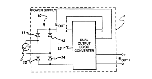
Figure 1 illustrates a power supply 1 of a type
well-known in the art for receiving an ac power line voltage
from an ac power source 2 and providing two independently
controllable output voltages Eouti and Eout2~ The power
supply 1 includes a full-wave rectifier 10, having diodes 11-
14 connected together in a full-bridge configuration, for
~~~9~
- 6 -
RD-20,722
providing a rectified ac line voltage to a typical dual-
output dc-to-do converter 15.
In accordance with the present invention, as shown
in Figure 2, by coupling one of the outputs, e.g. Eoutl. of
dual-output converter 15 in series with the rectified ac line
voltage, a high power factor power supply 4 for providing a
do output voltage Eout2 is realized.
Figure 3A illustrates one preferred embodiment of
an off-line switching power supply according to the present
invention for converting an ac power line voltage to a
regulated do output voltage. According to the embodiment of
Figure 3A, the power supply of the present invention includes
full-wave rectifier 10, having diodes 11-14 connected
together in a full-bridge configuration, coupled to ac power
source 2. Rectifier 10 provides a full-wave rectified
voltage between points b and o. As shown in Figure 3A, a
boosting converter output circuit 16 is coupled in series
with the full-bridge rectifier via a high-frequency filter
inductor Lin. Alternatively, high-frequency filter inductor
Lin may be connected on the ac side of rectifier 10, if
desired. The boosting converter output circuit 16 includes a
center-tapped boost transformer secondary winding 18 of a
boost transformer Tb coupled in parallel with a resonant
capacitor Cr. The boosting converter output circuit further
includes a center-tapped transformer, full-wave boost
rectifier comprising diodes 20 and 21, the anodes of which
diodes are connected to the respective terminals of the
resonant capacitor Cr. The cathodes of diodes 20 and 21 are
connected together at a point a which is connected to the do
link at potential Vao~
As shown in Figure 3A, a dc-to-ac converter 22
comprising a full-bridge connection of switching devices Q1-Q4
is connected between the do link and ground. The series
combination of a boost transformer primary winding 24 and a
~059~~
_7_
RD-20,722
resonant inductor Lr is coupled between the junction joining
switching devices Q1 and Q2 of converter 22 and the junction
joining a center-tapped pair of relatively large energy-
storage capacitors ~~. (Alternatively, capacitors 02n may be
S relatively small if the series combination thereof is coupled
in parallel with another energy-storage capacitor (not shown
which is relatively large.)
An alternative embodimen~ of boosting converter
output circuit 16, as shown in Figure 3B, includes a full-
wave bridge rectifier comprising diodes 6-9 and a single
secondary winding 17 of boost transformer Tb. Furthermore,
although boosting power converter output circuit 16 is shown
in Figure 3A as comprising a parallel resonant circuit, it is
to be understood that the advantages of the present invention
may also be realized using other resonant circuit
configurations. For example, a combination series/parallel
resonant circuit may be employed wherein another capacitor Cr2
(not shown) is coupled in series with resonant inductor L= on
either the primary or secondary side of transformer Tb. As
another example, a series resonant circuit configuration may
be employed wherein resonant capacitor Cr is situated in
series with resonant inductor L= ,on either the primary or
secondary side of transformer Tb, rather than in parallel
therewith as shown in Figure 3A.
The primary winding 26 of another transformer 27 is
coupled across the junctions joining the switching devices
Q1-Q2 and Q3-Qq of the respective full-bridge converter legs.
The respective terminals of the secondary winding 28 of
transformer 27 are connected to the anodes of diodes 30 and
31. The cathodes of diodes 30 and 31 are connected to an
output filter inductor 32 and an output filter capacitor 34.
The regulated do output voltage Eout is provided across
capacitor 34.
_ g _
RD-20,722
In operation, the boosting converter provides the
instantaneous voltage difference between the output voltage
pL~ of the full-bridge rectifier 10 and the do link voltage
Vao. The output voltage of the resonant boosting converter is
controlled by the switching frequency of full-bridge
converter switching devices Q1-Qq via a first ac signal
generated across the boosting converter resonant circuit L=
and C=, while the do output voltage Eaut is controlled by
pulse width modulation (PWM) of a second ac signal generated
across transformer 27, i.e. by phase-shifting the two legs of
the converter bridge with respect to each other. Because
phase-shifting the two full-bridge converter legs does not
affect the voltage applied to the resonant circuit Lr and Cr,
the boosting converter voltage Vab is independent of the power
supply output voltage Eout~ As a result, a fast transient
response is attained for the input boosting converter and the
power supply output voltage simultaneously.
A suitable control for the power supply of the
present invention is illustrated in Figure 4 and described in
Steigerwald and Kornrumpf U.S. Pat. No. 4,642,745, cited
hereinabove. (The reference numbers in Figure 4 correspond
to those in the Steigerwald and Kornrumpf patent.) The
Steigerwald and Kornrumpf patent describes a PWM control for
controlling the regulated do output voltage by adjusting the
duty cycle of the inverter output signal whenever an error is
detected between the commanded do output voltage Eout and the
actual do output voltage Eout. In addition, the Steigerwald
and Kornrumpf patent describes an active frequency control
wherein the actual converter input current is compared with a
commanded current in phase with the utility line voltage: any
difference causes a frequency adjustment for controlling a
boosting converter. Advantageously, since the boosting
converter and the power supply output voltage of the present
invention are completely decoupled, any adjustment of the do
RD-20,722
output voltage using the Steigerwald and Kornrumpf control
system will have no effect on the input current to the
converter of the present invention.
As another advantage, it has been found that even
with no active control of the ac line current, the power
supply of the present invention operates with a relatively
high power factor and low peak ac line current, due to the
favorable gain characteristics of the parallel resonant
circuit Lr and Cr. Near the valleys of the input ac current
waveform, low power is delivered, and the resonant circuit is
lightly loaded so that the boosting converter output voltage
can ring up to provide the high boost needed, i.e., the
difference between the low value of the instantaneous ac line
voltage IvLI and the do link voltage Vao. Conversely, near
the peaks of the input ac current waveform, higher power is
delivered and the resonant circuit is highly damped. As a
result, little boosting action is needed. Hence, the gain
characteristics of the parallel resonant boosting converter
naturally cause the power supply to yield a high power
factor. Advantageously, therefore, the power supply of the
present invention does not require active control of the
input ac current waveform in order to provide a high power
factor. The portion of the control 40 in Figure 4
represented by dashed lines 70 can thus advantageously be
eliminated, with the output of compensator gain block 69
being coupled to the input of ramp generator 58 (as shown by
the dashed line 71) via resistor 58, if desired, thereby
simplifying the controls required for the high power factor
power supply of the present invention.
As still another advantage, the boosting power
converter is not required to convert the entire power
delivered to the load. That is, for a do link voltage Vao
which is not substantially greater than the peak of the ac
input voltage, i.e. less than twice the peak of the ac input
- io -
RD-20,722
voltage, the peak rating of the boosting power converter is
less than the peak power delivered to the do link, as a
result of the series connection of the boosting converter in
the switching power supply. For example, for a do link
voltage Vao of approximately 25% above the peak of the ac line
voltage, the peak power converted by the boosting converter
is approximately 78% of the full power delivered, and the
average power processed by the boosting converter is
approximately 59% of the full power delivered.
Figure 5 illustrates another aspect of the power
supply of the present invention that is especially suitable
for applications wherein a self-contained ac-to-do "front-
end" converter is desirable, e.g. to supply a do bus in a
distributed power system or to retrofit existing low power
factor switching power supplies. As shown in Figure 5, the
center-tapped energy-storage capacitors ~ of Figure 3A have
been replaced by a single equivalent energy-storage capacitor
Cin, and a dedicated resonant half-bridge converter 80 has
been coupled thereacross. (Alternatively, a full-bridge
converter such as that of Figure 3A comprising switching
devices Q1-Q4 may be used.) Converter 80 includes the series
combination of switching devices Ql and QZ with the resonant
circuit comprising the series combination of boost primary
winding 24, resonant inductance Lr, and capacitance Cb (or,
alternatively, a pair of capacitors ~ coupled in parallel as
shown in Figure 3A for capacitors ~) at the junction between
switching devices Q1 and Q2. The resonant boosting converter
of Figure 5 may be controlled by the switching frequency of
half-bridge converter switching devices Q1 and Q2, a suitable
frequency control being described in the Steigerwald and
Kornrumpf patent, U.S. Pat. No. 4,642,745, cited hereinabove.
As an alternative, the resonant boosting converter could be
controlled by suitable PWM control.
..
- 11 -
RD-20,722
While the power converter of the present invention
has been described with reference to power supplies including
dual-output converters, the outputs of which are either
resonant frequency controlled, PWM controlled, or a
S combination thereof, it is to be understood that any type of
dual-output power converter can be used in a power supply in
accordance with the present invention to achieve the
advantages thereof. Hence, while the preferred embodiments
of the present invention have been shown and described
herein, it will be obvious that such embodiments are provided
by way of example only. Numerous variations, changes and
substitutions will occur to those of skill in the art without
departing from the invention herein. Accordingly, it is
intended that the invention be limited only by the spirit and
scope of the appended claims.