Note: Descriptions are shown in the official language in which they were submitted.
WO 91/02242 PCT/FR90/00608
Self-supporting thin-film filament detector process for
its manufacture and its applications to qas detection and
qas chromatoqraphy
The present invention concerns a filament type
sensor for determining a static or dynamic characteristic
of a gas environment such as the air, for example, a
method of fabricating it, and applications of the sensor
primarily to the detection of oxidizable gases but also
to gas chromatography (de~ection of ionizable gases) and
fluid flowrate measurement.
A filament type sensor of this kind comprises a
resistive element within a filament adapted to exchange
heat with the environment and an interface area adapted
to react with the environment in a physico-chemical
process ~in the broadest possible sense of the term:
catalysis of combustion, adsorption, ionization, simple
thermal exchange) influencing an electrical
characteristic of the interface area (temperature or
resistance, voltage, current, etc) according to the
; 20 characteristic of the environment to be determined
(concentration, flowrate, etc). The interface area can
be the external portion of the resistive element, or a
catalyst film heated by conduction, or a separate
electrode.
Some sensors of this kind are based on measuring
the heat exchanged (detection o~ combustible gases,
flowmeter, etc) and may be characterized as calorimetric
sensors; there are also various filament type sensors
having the common feature of measuring a concentration,
based on various phenomena (measurement of the heat
exchanged in the case of detecting combustible or
oxidizable gases, for example, measurement of the
; quantities of ions captured by an electrode in gas
chromatography, for example, etc). Filament type sensors
are therefore of very diverse kinds, both with regard to
.
,
Wo 91/02242 PCT/FR90/00608
2 ~ $ 3
the physico-chemical phenomenon on which their operation
is based and with reyard to the nature of the parameter
to be measured.
Although the remainder of this description refers
for the most part to the detection of an oxidizable gas
in a gas environment such as the air, in the field of
explosimetry, for example, this is a pxeferred
application and is not limiting on the invention.
A known way of detecting an oxidizable gas in the
air uses a filament, usually of platinum, heated by the
Joule effect, ice. by the passage of an electric current.
The oxidizable gas contained in the surrounding air is
oxidized by catalysis in contact with the filament, so
that the latter is further heated. The resulting
temperature variation causes a variation in the
resistance of the filament, which is measured directly or
indirectly to obtain the concentration of said oxidizable
gas in the air. These filament-based detectors are
largely hand-made. They therefore suffer from lack of
reproducibility and high cost. Their low electrical
resistance and their low surface area/volume ratio make
it necessary to operate them at high temperatures (around
1 O00C).
Other oxidizable gas detectors are based on
catalytic beads; they are formed by a metal detector (of
platinum, for example) coated with alumina doped with a
catalyst, and resemble a small pearl. These detectors
age less rapidly, as the associated combustion
temperature is lower. However, these beads have the
disadvantages of significant drift in sensitivity,
reduced stability and an increased response time as
compared with filaments.
A third type of oxidizable gas detector is based on
semiconductor metal oxides doped with a catalyst. These
detectors are formed by a metal heating element which
: . ~ : :
WO 91/02242 PCT/F~90/006~8
3 ~ 3
heats an insulative material (alumina, for example)
sleeve onto which is deposited a film of semiconductor
material whose resistance varia~ions are measured. These
detectors are sensitive to any gas that can be adsorbed
onto the surface of the semiconductor. They have a
relatively long response time, however, and the further
disadvantage of high electrical power consumption; also,
the effects of humidity are not compensated.
The invention is directed to alleviating the
aforementioned disadvantages by improving reproducibility
and by reducing thermal lvsses from the filament by
conduction, whilst also reducing manufacturing costs.
In a very general way, the invention proposes a
filament type sensor for determining a static or dynamic
characteristic of a surrounding environment, comprising a
resistive element adapted to be heated in ~he environment
by the Joule effect and an interface area adapted to
react with the environment in a physico-chemical process
influencing an electrical characteristic of the interface
area according to the characteristic to be determined,
characterized in that it comprises a supporting wafer
through which there is formed at least one hole and at
least one filament including the resistive element,
comprising one or more thin films and having a central
portion situated in the hole and at least two end
portions by which the central portion is connected to the
supporting wafer.
In other words, the invention proposes a filament
fabricated using microelectronics technologies in such a
way that it is "self-supporting~, meaning that the only
connections between it and the support are thin films:
the filament is therefore constituted of one or more
"floating~' thin films, which considerably reduces thermal
losses by conduction.
The invention results from the observation that
-
.
:~ .
,
WO 91/02242 PCT/FR90/00608
2 ~ 3
thin film ~echnology can be used to produce a filament
having sufficient mechanical strength and thermal shock
resistance for it to be self-supporting.
The applicants have observed that, in a surprising
manner, despite the thinness of the filament which
confers upon it the necessary electrical resistance, it
is both sufficiently sensitive with respect to the
physico-chemical reaction on which the measurement is
based and sufficiently strong that it is not worn out
prematurely through contact with the surrounding
environment.
According to preferred features of the invention:
- the filament is formed by a film of a metal
catalyst whose exterior surface constitutes said
interface area,
- at least the central portion of the filament is
formed by at least three superposed thin films comprising
a conductive material film extending to the ends of the
filament, a catalyst film forming the interface area and
an electrically insulative material intermediate film,
- the resistiYe element of the filament is a film
of a noble metal such as platinum, gold or palladium or a
combination of noble metals,
- the filament has a sinuous shape, for example a
crenellated shape,
- the central portion of the filament is connected
to the substrate by more than two end portions,
- the substrate is chosen from the group of
materials comprising glass, silicon, alumina, silica,
quart~ and polymers,
- the interface area is a thin film deposited on at
least one surface of the substrate near the hole.
The invention also proposes a filament preparation
method using microelectronics technology suitable for
fabricating the aforementioned sensor and characterized
- , .:
WO 91/02242 PCT/FR90/00608
in that it comprises the following stages:
- depositing onto the front and rear surfaces of a
wafer-form substrate a thin film front mask incorporating
- a front window the shape of which reflects the shape of
the filament to be fabricated and has a central portion
extended by end portions, and a thin film rear mask
incorporating a rear window facing the central portion of
the window excluding said ends, but larger than this
central portion,
10- hollowing a trench into the substrate by etching
the front surface of the latter through the front mask,
- depositing onto the back of this trench one or
more thin films adapted to constitute the filament, at
least one of said thin films being an electrically
conductive material, and
- eliminating the substrate to its full thickness
by etching it through the rear mask.
According to preferred features:
- before the substra~e is etched through the rear
mask to eliminate its entire thickness, a protective film
is deposited onto the front surface and into the trench
and the protective film is eliminated after the substrate
is etched,
- the protective film on the front surface is a
polymer resin,
- the front mask comprises an intermediate film
covered with a film of resin, the thin film(s) of the
filament being deposited, after elimination of the resin
film, by depoæition of one or more thin films into and
around the trench followed by elimination of the thin
film(s) deposited outside the trench by etching the
intermediate film.
The main advantages of the invention as compared
with all the previously mentioned detector elements are
very low electrical power consumption and a very short
,
:
: . . , ~ : . . :
:'~ . : : . . .
::
WO 91/02242 PCT/FR90/00608
6 2 ~ 3
response tîme.
The sensor can be manufactured automatically and in
multiples and can therefore be fabricated reproducibly
and in large quantities at low cost.
Its resistance depends on its geometrical shape and
allows an operating temperature lower than conventional
filament type sensors, which results in good measurement
resolution and slower ageing. It is relatively
insensitive to impact due to its novel construction and
its resulting very low mass.
Because its thermal inertia is very low, it can be
used for measurements at different temperatures and in
very short time intervals.
The invention also consists in applications of a
sensor of this kind, principally to detecting oxidizable
gases such as methane or carbon monoxide and also to gas
chromatography (detection of ionizable gases) and to the
calorimetric measurement of gas flowrates.
Objects and features of the invention will emergs
from the description of the drawings, in which:
- figure 1 is a perspective view of a sensor in
accordance with the invention,
- figure 2 is a partia~ view of another sensor in
longitudinal cross-section in the direction of its
thickness,
- figure 3 is a variant of figure 1, and
- figures 4 through 9 are views of the sensor from
figure 1 in cross-section at various stages in its
fabrication on a substrate by the method in accordance
with the invention.
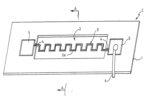
The sensor C in figure 1 comprises a support wafer
1 made from glass or some other insulative (or
semiconductor) material with a hole 2 through it. As an
alternative the supporting wafer may be made from an
insulative or non-insulative material covered with an
'
WO 91/02242 PCT/FR90/00608
insulative film.
Across the hole is a filament 3 in the form of a
thin film of an electrically conductive material whose
outer surface or skin constitutes an interface area with
the surrounding environment.
The filament 3 has a central portion 3A and
electrically conductive ends 4 by which the central
portion 3A is connected to the supporting wafer. The
ends terminate at conduc~ive lands 5 to which electrical
wires connacting the sensor to the remainder of the
electric circuit including it can he connected, by
soldering, for example.
The ~ilament 3 preferably has a sinuous shape
parallel to the supporting wafer, in this instance a
crenellated shape. For a given cross-section and a given
distance between the lands 5 this increases its surface
area and reduces the risk of rupture due to thermal
expansion. Other geometrical shapes are possible, of
course. The thin film filament need not be rectilinear
overall, but could be curved parallel to the supporting
wafer. The filament could equally well be in the form of
a thin plate parallel to the supporting wafer, with
dimensions less than those of the hole, of course.
The thin film 3 may be produced from any substance
giving rise to the physico-chemical phenomena on which
the measurements are based; in this instance the thin
film is made from a material chosen to have electrical
properties which are modified by the environment to ~e
characterized.
In the particular instance of oxidizable gas
measurement it may be a catalyst platinum, nickel,
osmium, gold, irridium, combinations of metalst metal
oxides, semiconductors, sulfides, etc.
The material may also be chosen according to its
absorbent or adsorbent properties if they modify its
WO 91/02242 PCT/FR90/00608
electrical characteristics.
In figure 2 parts similar to parts of figure 1 have
the same reference number with a ~prime" suffix. This
figure shows another sensor C~ whose filament 3~ is not a
single thin f~lm but a stack of ~hin films of conductive
or insulative material or catalyst. The succession of
these films is such that:
- each catalyst film is at the top or bottom of the
stack r
- each electrically conductive film is electrically
connected to the lands 5, and
- an insulative film is provided between the
conductive material or catalyst films.
To be more precise, figure 2 shows three successive
films 7l 8 and 9 respectively of conductive material,
insulative material and catalyst. In an alternative
embodiment that it not shown the films are stacked with a
9-8-7-8-9 arrangement.
In figure 3 parts similar to parts of figure 1 have
the same reference number with a ~quote mark~ suffix.
The figure shows ano~her variant C" of figure 1 in which
additional end portions 10 are disposed transversely to
the central portion of the filament 3". These additional
portions end at lands lOA. In the case of a single-film
filament as in figure 1, they can be used for
intermediate electrical measurements or in different
circuits, so reducing the number of different sensors to
be manufactured and stored for a given number of
applications. In the case of a multiple film filament as
in figure 2, these portions 10 may be electrical
connections to the catalyst film which is otherwise
insulated from the conductive film.
It will be understood that in each of the foregoing
examples all of the filament is entirely contained within
the overall thickness of the substrate.
WO 91/02242 PCT~YR90/00608
2 ~ ~f~ 3
Figures 4 through 9 show in cross-section on the
line A-A in figure 1 various stages in the manufacture of
the sensor 1, a glass substrate being used in this
example:
A first phase entails preparing the substrate 1 by:
- cleaning it using nitric or sulfochromic acid, for
example, followed by rinsing with deionized water,
- drying under dust-~ree conditions.
In a second phase masks are prepared on each of the
front and rear surfaces lA and lB of the substrate, in
stages, as follows (see figure 4):
- a thin film 11 of chromium with a thickness of
1 000 to 2 000 A is deposited onto the rear
surface; a fi.lm 12 of chromium between a few A and
1 000 A thick and then a film 13 of gold
approximately 1 000 A thick are deposited onto the
other (front) surface; these stages may be
staggered with respect to each other but are
preferably simultaneous;
- a film 14, 15 of photosensitive resin is deposited
onto each side of the substrate,
- exposure masks 14A and 15A are positioned in face-
to~face relationship on opposite sides of the
substrate and the aforementioned films, after which
the films 14 and 15 are exposed through the masks
14A and 15A and the exposed areas are developed:
this produces resin masks 16 and 17; these last two
stages are entirely conventional;
- the meta.l. films are etched through the masks 16
and 17:
. etching of the chromium film 11 on the rear
surface,
. etching of the gold film 13 on the front
surface,
. etching of the chromium film 12 on the front
.
- .
WO 91/02242 PCT/FR90/00608
surface;
- further rinsing with deionized water; the result
is the structure shown in figure 5.
It will be understood tha~ the rear mask obtained
in this way (films 11 and 14) includes a window 16A
facing the ~entral portion (between the ends 4 and 5 in
figure 1) of the window 17A in the front mask ~films 12,
13 and 15), to the exclusion of said ends, but the window
16A is larger (in this instance wider on each side) than
the central portion.
In a third phase hydrofluoric acid is used to etch
trenches 18 and 19 into the glass through the masks
consisting of the superimposed films of chromium 12, gold
13 and resin 15 etched onto the front surface lA of the
wafer 1. This etching is isotropic (in the direction of
the thickness and laterally); the resulting undercutting
leaves the films 12 and 13 projecting over the inclined
edges 20 of the trench to form an overhang 21. Although
it is standard practice with etching methods of this type
to modify the process conditions to avoid such
undercutting, in this instance such undercutting is
deliberate and useful. The resulting overhang 21 allows
improved removal of the films 12 and 13 at the end of
fabrication.
The resin masks 14 and 15 are removed, for example
using acetone and then nitric acid. The resulting
structure is then rinsed with deionized water and dried
under du~t-free conditions, yielding the structure from
figure 6.
In a Eourth stage the filament 3 is Eormed at the
bottom of the trench 18 by depositing a thin film 23 of
chromium (approximately 100 A thick) onto the fxont
~ surface lA of the substrate, including onto the bottom of
; the trench 18/ followed by the deposition of a film 24 of
platinum ovex all of the thin film 23 (see figure 7).
' ' '
~; .
`~
WO 91/02242 PCT/FR90/0060B
There are obtained in this way thin films 23A and 24A of
gold and platinum in the trench dissociated from portions
23B and 24B of gold and platinum deposited on the
remainder of the front surface. The overall thickness of
the films 23 and 24 must therefore be (at least slightly)
less than the depth of the trench 18. In the case of the
sensor C' from figure 2 the equivalent condition is that
the overall thickness of the deposited films must be less
than the depth of the trench. It is essential that the
films in the trench 18 do not come into contact with the
overhangs 21.
The side portions 24A and 23A of the excess
platinum and chromium films are then eliminated by
chemical e~ching of the gold film 13 (immersion of the
subs~rate for at least three hours in a gold etching
reagent ~hich eliminates mechanically the superfluous
film of platinum, with the final traces of excess
platinum removed in an ultrasonic cleaning tank). This
operation is greatly facilitated by the overhang 21
obtained by undercutting.
Following rinsing with deionized water and drying a
new film 25 of photosensitive resin approximately 3 ~m
thick is deposited onto the rear surface and is then
exposed through the same mask as in figure 4: following
development, a rear mask is obtained coincident with the
chromium mask 11 remaining on this surface; in practise
the mask is then cured at 140C for 30 minutes.
In a final phase the substrate is hollowed out
through its entire thickness by an etching process
through the rear mask, in the following stages:
- a protective film 26 is deposited on the front
surface lA covered with the chromium film 12; this
protective film fills the trench 18 and by adhering to it
covers the filament at its bottom; this protective film
may be of any material which is resistant to hydrofluoric
. ... ~ .::
WO 91/02242 PCT/FR90/00608
12 c
2 ~
acid and can be easily dissolved using a commercially
available solvent; a ZIVI APIEZON-W type polymer resin is
preferably used;
- the glass 1 carrying the filament is chemically
etched with ultrasonic agitation through the mask 25
deposited onto the rear surface lB and consisting of the
chromium film 11 and the etched photosensitive resin
film 25.
After the glass and the protective film 26 are
removed using an appropriate commercially available
solvent, such as perchlorethylene, for example, the
filament 3 is, surprisingly, found to be ~self-s~pported~
in the glass wafer (see figure 9). All traces of resin
and polymer are removed from the glass wafer using an
appropriate chemical reagent (usually fuming nitric acid)
and the remaining chromium films 11 and 12 on each side
of the glass wafer are removed using the reagent for
chemical etching of chromium.
The inclined flanks of the hole 2 in figure 9
result from the isotropic nature of the etching by
hydrofluoric acid. In the case of a ~ubstrate and an
acid producing anisotropic etching, vertical flan}cs would
be obtained as shown in figures 7 and 8.
Specific examples of the chemical etching :reagents
used are:
. chromium: 1) SOPRELEC ( EVRY ) Cr-ETCH
2) 50 g/l of KMn04 + 50 g/l of ROH ~ 1 1
of deionized water,
. gold: 25 g/1 of 12 = 60 g/l of KI + 1 1 of
deionized water,
. glass: HF diluted 40% to 20% (according to the
required etching rate).
Examples of thicknesses for glass wafers 150 ~m
thick are:
. chromium No 11 : 500 to 1 000 ~,
~: .
'
W0 91/02242 PCT/FR90/00608
13
. chromium Nos 1~ and 23 : 50 to 500 A,
. gold No 13 : 1 500 to 2 500 A,
. platinum : O.5 to 9 ~m,
. W apiezon : 100 ~m minimum,
. SHIPPLEY 1350-H photosensitive resin O 1 to 3 Im,
. length of hole : 2 ~m~
The benefits of the chromium films are firstly the
improved deposition of gold, which could not be achieved
directly onto the glass, and secondly the high strength
1~ of the mask formed by the photosensitive resin and
chromium films during etching of the glass with
hydrofluoric acid.
In a variant o~ the method shown in figure 5bis and
6bis the gold layer is thickened. This makes it possible
to deposit a greater thickness of platinum.
The second and third phases of the method are
modified as follows:
After etching the metal through the masks 16
and 17:
- the resin layers 14 and 15 are cleaned using
acetone and nitric acid,
- further rinsing is then carried out using
deionized water.
It will be realized that the resulting rear mask
(layer 11) comprises a window 16A facing the central
portion (between the ends 4 in figure l~ of the window
17A in the front mask (layers 12, 13) excluding said ends
but that this window 16A i.s wider (in this instance wider
` on each side) than the central portion.
`~ 30 The gold film 13 is then thickened (figure 5bis) by
electrolytically depositing gold (film 13bis) followed by
rinsing with deionized water.
~i~ The thickness of the electrolytic gold plating is
determined by the depth of the trenches to be etched in
the next stage and is approximately 1 ~m for a trench
" ,
:~
~'
WO 91/02242 PCT/FR90/00608
14 2~
depth of 10 to 15 Im. A uniform film llbis of protective
photosensitive resin is deposited onto the r~ar surface.
In the third phase hydrofluoric acid is used to
etch the trench 18 into the glass through the mask
consisting of the superimposed films 12 of chromium and
13 and 13his of gold etched onto the front surface lA of
the wafer 1. This etching is isotropic (in the direction
of the thickness and laterally); the resulting
undercutting leaves the films 12, 13 and 13bis projecting
over the inclined edges 20 of the trench to form an
overhang 21. Although it is standard practice with
etching methods of this type to modify the process
~onditions to avoid said undercutting, in this instance
such undercutting is deliberate and useful. The
resulting overhang 21 allows improved removal of the
films 12 and 13 at the end of fabrication.
The resin mask llbis is removed, for example using
acetone and then nitric acid. The resulting structure is
then rinsed with deionized water and dried under dust-
free conditions, yielding the structure of figure 6.
Subsequent stages of the process are exactly thesame as before.
In addition to glass it is possible to use other
substrates: silicon, alumina, silica and especially
quartz which offers good heat resistance and selective
resistance to etching.
It is also possible to use double-sided metal-
plated substrates (gold over chromium, for example) which
means that the irs~ metat deposition stages can be
dispensed with.
Trials have been conducted on quartz between 125
and 175 ~m thick plated with gold over chromium on both
sides using the same chemical etchant reagents.
There are diverse application~ for a sensor of this
kind.
WO 91/02242 PCT/FR90/00608
2~ 3~
Firstly, it can be used to detect oxidi~able gas by
integrating a described known circuit.
It can also be used Eor chromatographic
measurements: the filament 3 is used to heat and locally
ionize the gaseous medium and one or more ion receiving
electrodes (interface area) are constituted by one or
more conductive thin films deposited onto the substrate
near the hole 2: the chromium films 11 and 12 may be left
in place for this purpose.
It goes without saying that the present inven~ion
has been described by way of non-limiting example only
and that numerous variants can be put forward by the man
skilled in the art without departing from the scope of
the invention. For example, multiple filaments may be
formed in a single hole and multiple holes may be formed
in a single substrate ~collective fabrication).
,
..
: : .,
: ' ~