Note: Descriptions are shown in the official language in which they were submitted.
CA 020603~4 1998-09-11
BACKGROUND OF THE INVENTION
This invention relates in general to induction motor
drive systems and, more particularly, to an induction motor
drive system for operating a single-phase, two winding
induction motor from a two-phase power supply circuit.
A conventional split-phase capacitor start or
capacitor run single phase induction motor, also known in
the art and referred to hereinafter as a permanent split
capacitor (PSC) motor, has two stator windings, a "main"
winding and a "start" winding. Fig. 1 illustrates an ~
exemplary PSC motor 100 that includes a main winding 102
and a start winding 104 that are commonly connected at one
end. Main winding 102 and start winding 104 are mounted in
the stator (not shown) of motor 100 and spatially separated
from each other by an angle related to the rated speed of
motor 100, e.g., 90~ for a two pole, 3600 RPM motor, as is
well known in the art. Such PSC motors are designed to be
operated with a run capacitor, such as a run capacitor 106,
connected in series with start winding 104. It is a
typical practice in the industry for the motor manufacturer
to not supply the run capacitor with the motor, but instead
to only specify parameters of the capacitor, e.g.,
capacitance and power rating, sufficient to enable a user
to procure and install the capacitor.
In the operation of PSC motor 100, main winding 102
and the series combination of start winding 104 and run
capacitor 106 are connected in parallel with each other and
directly across a single phase power source 110. Since
start winding 104 is energized through capacitor 106, the
phase angle of the current flowing through start winding
-1-
CA 020603~4 1998-09-11
104 is shifted with respect to the current flowing through
main winding 102, such that the phase angle between the
respective currents flowing in windings 102 and 104 is 90~
while the motor is running. The phase angle between the
currents in windings 102 and 104 and the spatial separation
of those windings result in the creation of a rotating
magnetic field which is inductively coupled to the rotor
(not shown) of motor 100, to exert a rotational force on
the rotor.
The rotor of motor 100 attempts to rotate in
synchronism with the rotating magnetic field but lags the
rotating magnetic field by a "slip" factor, resulting in a
torque on the rotor which is in part proportional to the
amount of slip.
The starting torque exerted on the rotor of motor 100
during a starting period when motor 100 is started and
accelerated to rated speed is also proportional to the sine
of the phase angle between the currents flowing in windings
102 and 104. Therefore, in order to maximize the starting
torque, it is necessary to achieve a phase angle of 90~
during staring. However, the starting torque for a single
phase PSC motor, such as motor 100, is generally poor
because the specified parameters of the run capacitor are
only optimized for running conditions, not starting
conditions. Thus, the capacitance of run capacitor 106 is
specified by the manufacturer based on the impedances of
windings 102 and 104 that will be experienced during
running of motor 100, rather than during starting.
However, as known in the art, the apparent values of motor
winding impedances vary during the starting period of a PSC
--2--
CA 020603~4 1998-09-11
motor and are therefore different during starting than
during running. As a result of the capacitance of
capacitor 106 being optimized for running and not for
starting, its magnitude is too small for starting. This
results in the phase angle between the currents flowing in
windings 102 and 104 being less than 90~ during the
starting period and the starting torque being less than a
maximum possible starting torque.
One solution known in the art to compensate for the
insufficient magnitude of capacitor 106 during starting is
to connect a starting capacitor 112 across capacitor 106 to
increase the total capacitance in series with start winding
104 and thereby increase the current flowing in the start
winding, the phase angle and the starting torque of motor
100. Starting capacitor 112 is disconnected, e.g., by
means of a centrifugal switch, positive temperature
coefficient thermistor (PTC device) or relay, once the
motor has reached running speed. Disadvantageously,
although operation of starting capacitor 112 generally
improves the starting torque of motor 100, its use still
does not maximize torque throughout the starting period of
motor 100. Ideally, the magnitude of the capacitance in
series with start winding 104 would have to be continuously
varied during the start period to maintain a desired phase
angle while the respective impedances of windings 102 and
104 vary.
Conventional single phase PSC motors are commonly used
in heating, ventilating and air-conditioning (HVAC) systems
to drive system loads such as fans, pumps and compressors.
HVAC systems are subject to widely varying demand cycles
-3-
CA 020603~4 1998-09-11
- due to a variety of factors such as, for example, daily and
seasonal fluctuations of ambient temperature, human
activity in the controlled environment and intermittent
operation of other equipment in the controlled environment.
Accordingly, in order to assure a satisfactory temperature
of the controlled environment, the HVAC system must have
the heating and/or cooling capacity to accommodate "worst
case" conditions. As a result, under less than worst case
conditions the HVAC system has a significant over-capacity
and is necessarily operated at reduced loading. Since the
maximum operating efficiency of a motor, such as a PSC
motor, is normally obtained only when the motor is
operating at full load, the reduced HVAC system load
results in inefficient operation of the motor. Further, to
the extent that motors are required to cycle on and off to
meet HVAC load requirements less than the capacity of the
HVAC system, further significant operating inefficiencies
are experienced. Such further inefficiencies include the
operating cost of frequent starting of motors as well as a
reduction in useful life of such motors resulting from the
well known thermal and mechanical stresses, experienced
during starting.
A solution for overcoming the above inefficiencies
resulting from the excessive capacity of an HVAC system is
to vary the system capacity to meet the demand on the
system. One method for varying HVAC system capacity is by
varying the speed of the motors driving the HVAC system
loads in accordance with the demand. With respect to HVAC
system loads driven by single phase motors, such as PSC
motors, in order to effect a desired motor speed control,
--4-
CA 020603~4 1998-09-11
it would be necessary to vary the frequency of the single
; phase power supplied to the motor. However, with respect
to PSC motors, the run capacitor, e.g., capacitor 106 of
motor 100 (Fig. 1), is optimized for a particular set of
running conditions, including operation at a nominal
frequency, e.g., 60 Hz. As a result, operation of a PSC
motor at other than the nominal frequency results in
production of less than optimal torque and inefficient
operation. While some applications may exist in which very
limited speed control of a PSC motor is achieved by a small
variation of the single phase source frequency, such
variation from the nominal frequency results in less
efficient operation since the motor is nevertheless
designed for optimum performance at the nominal source
frequency.
A conventional implementation of varying motor speed
to modulate HVAC system capacity typically requires a two-
or three-phase motor supplied with two- or three-phase
power, respectively. The use of such polyphase motors and
power supplies enables variation of motor speed by varying
the frequency of the voltage applied to the motor while
maintaining a constant volts/frequency (volts/hertz) ratio.
Maintenance of a constant volts/hertz ratio corresponds to
maintenance of a constant air gap flux and efficient motor
operation while delivering rated torque. The use of
polyphase motors also offers several other advantages over
that of a single phase motor such as, for example, lower
locked rotor currents, higher starting torque, lower full
load currents and improved reliability due to elimination
of the start and/or run capacitor which are required in
-5-
CA 020603~4 1998-09-11
single phase motors. Disadvantageously, such polyphase
motors are more expensive than single phase motors having
the same horsepower rating.
Such applications employing polyphase motors generally
require provision of variable frequency polyphase power
from either a single phase or polyphase line source by
means of a power supply circuit, including a polyphase
inverter, coupled between the motor and the line source.
One drawback to this arrangement occurs in the event that
the power supply circuit fails and it is not possible to
connect the polyphase motor directly to the line source,
such as, for example, when a three-phase motor is driven by
an inverter which receives power from a single phase line
source. Failure of the power supply circuit therefore
results in failure and unavailability of the system
utilizing the polyphase motor.
Previous attempts to address the problem of backup
power for polyphase motors fed from a single phase power
source have required inverter redundancy or additional
circuit means for temporarily directly connecting the
polyphase motor to the single phase power source. However,
the additional circuit means required to "simulate"
polyphase power may not provide truly polyphase power and
therefore may not drive the polyphase motor at optimum
efficiency.
SUMMARY OF THE INVENTION
It is an object of the present invention to provide an
AC motor drive system which overcomes the aforementioned
problems and disadvantages of conventional drive systems.
-6-
CA 020603~4 1998-09-11
To achieve the objects and in accordance with the purpose
of the invention, as embodied and broadly described herein
the invention is directed to an AC motor drive system for
driving an AC motor having a first winding and a second
winding, the first winding having first and second ends and
a first winding impedance and the second winding having
first and second ends and a second winding impedance that
is greater than the first impedance. The drive system
comprises two-phase power supply means for converting an
inputted power supply voltage into a two-phase AC output
voltage. The two-phase power supply means has a common
terminal, a first phase output terminal, and a second phase
output terminal. The common terminal of the two-phase power
supply means is adapted for connection to the respective
first ends of the first and second windings. The first and
second phase terminals of the two-phase power supply means
are adapted for connection to the second ends of the first
and second windings, respectively. The two-phase power
supply means converts the inputted power supply voltage to
a two-phase voltage provided on the first, second and
common terminals to drive the motor.
In accordance with an embodiment of the invention, the
two-phase power supply means includes a pulse width
modulated (PWM) inverter system and the inputted power
supply is an AC power supply. The drive system includes
means for rectifying the inputted AC power supply to
provide a DC supply voltage. The PWM inverter system
includes a three-phase inverter circuit including input
terminals coupled to receive the DC voltage and three
output terminals respectively corresponding to the common,
--7--
CA 020603~4 1998-09-11
first phase and second phase terminals. The PWM system
also includes switching means, included in the three-phase
inverter circuit, for inverting the DC voltage into the
two-phase output voltage, and voltage control means for
generating switching control signals for controlling the
operation of the switching means such that a first phase of
the two-phase output voltage is generated between the first
phase and common terminals and a second phase of the
two-phase output, voltage is generated between the second
phase and common terminals.
In accordance with another embodiment of the
invention, the AC motor drive system is adapted for
connection to a single-phase AC power supply having a line
conductor and a neutral conductor. The drive system
includes two-phase power supply means, including a line
terminal for coupling to the line conductor of the single-
phase power supply, for converting the single-phase power
supply into a two-phase output voltage. The two-phase
power supply means has a first phase output terminal and a
second phase output terminal. The respective first ends of
the first and second winding of the motor are connected to
a neutral terminal of the drive system for connection to
the neutral conductor of the single-phase power source.
The second ends of the first and second windings of the
motor are respectively coupled to the first and second
phase terminals of the two-phase power supply means.
Additional objects and advantages of the invention
will be set forth in part in the description which follows,
and in part will be obvious from the description, or may be
learned by practice of the invention. The objects and
--8--
CA 020603~4 1998-09-11
advantages of the invention will be realized and attained
; by means of the elements and combinations particularly
pointed out in the appended claims.
BRIEF DESCRIPTION OF THE DRAWINGS
The accompanying drawings, which are incorporated in
and constitute a part of this specification, illustrate
several embodiments of the invention and together with the
description, serve to explain the principles of the
invention.
Fig. 1 is a schematic diagram showing a conventional
PSC motor coupled to a single-phase power supply;
Fig. 2 is a schematic diagram illustrating a motor
coupled to a two-phase power supply in accordance with an
embodiment of the present invention;
Fig. 3 illustrates a motor drive system constructed in
accordance with an embodiment of the present invention;
Fig. 4 illustrates a power switching device included
in an inverter circuit shown in Fig. 3;
Fig. 5 is a phasor diagram illustrating voltages
produced by the inverter circuit of Fig. 3;
Fig. 6 is a block diagram of a circuit for controlling
the operation of the inverter circuit of Fig. 3;
Fig. 7 is a graphical illustration of voltage
waveforms produced during operation of the circuits shown
in Figs. 3 and 6;
Figs. 8A and 8B are graphical illustrations of voltage
waveforms produced during operation of the inverter circuit
shown in Fig. 3;
CA 020603~4 1998-09-11
Fig. 9 is a block diagram of an alternate embodiment
of the circuit shown in Fig. 6;
Fig. 10 is a graphical illustration of voltage
waveforms produced during operation of the circuit shown in
Fig. 9;
Fig. 11 illustrates a motor drive system constructed
in accordance with another embodiment of the present
invention; and
Fig. 12 is a block diagram of a control circuit for
use in the system shown in Fig. 11.
DESCRIPTION OF THE PREFERRED EMBODIMENTS
Reference will now be made in detail to the present
preferred embodiments of the invention, examples of which
are illustrated in the accompanying drawings. Wherever
possible, the same reference numbers will be used
throughout the drawings to refer to the same or like parts.
In accordance with illustrated embodiments of the
present invention, an induction motor drive system is
provided in which a two winding, single-phase induction
motor, such as a PSC motor is coupled to a two-phase power
supply circuit such that the two motor windings are
respectively connected to the two-phases of the power
supply circuit. The power supply circuit is configured and
operated to provide voltages that result in achieving an
optimum phase angle between the motor winding currents
during starting and running of the motor. The power supply
circuit is further operated to provide variable speed
operation of the single-phase motor while maintaining a
constant volts/hertz ratio at all operating speeds.
--10 -
CA 020603~4 1998-09-11
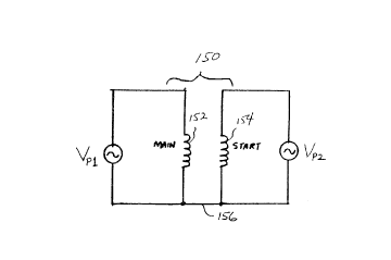
Referring now to the drawings, Fig. 2 diagrammatically
illustrates a two winding, single-phase induction motor 150
coupled to a two-phase power source provided in accordance
with an embodiment of the present invention. Motor 150
includes two stator windings, i.e., a main winding 152 and
a start winding 154 that are commonly connected at a common
winding node 156. Windings 152 and 154 of motor 150 are
connected across a first phase voltage Vp1 and a second
phase voltage Vp2 of a two-phase power source. The
two-phase power source is preferably configured and
operated to provide phase voltages Vpl and Vp2 with a desired
phase angle therebetween, for example 90~, that results in
optimum performance of motor 150.
Motor 150 is preferably provided as a conventional PSC
motor that does not include a run capacitor. As a result,
in accordance with the features of conventional PSC motors,
winding 154 is provided with a smaller conductor size and
has a greater number of winding turns than winding 152, so
that the impedance of winding 154 is greater than that of
winding 152. Another characteristic of conventional PSC
motors is that during operation from an AC source, a larger
voltage is applied across the start winding than across the
main winding. This difference in winding voltages results,
in part, from the connection of the run capacitor in series
with the start winding. For example, with respect to a
conventional 230VAC PSC motor connected through a run
capacitor to a single-phase 230VAC, 60Hz source, the
voltage applied across the main winding would be
approximately 230V, while the voltage applied across the
start winding could be on the order of 20~ higher or 276V.
-11-
CA 020603~4 1998-09-11
In view of this difference between winding voltages,
it is a feature of the illustrated embodiments of the
present invention that the two-phase power source, to which
motor 150 is connected, be configured and operated to
provide Vp2 > Vpl. The relative magnitudes of phase voltages
Vpl and Vp2 are preferably selected to duplicate the voltages
that would otherwise be experienced by the main and start
windings of motor 150 if it was operated at its rated
voltage and frequency as a conventional PSC motor including
a run capacitor in series with the start winding. However,
during variable speed operation of motor 150, the drive
system of the invention varies the absolute magnitudes of
voltages Vpl and Vp2 to maintain a substantially constant
ratio of volts/hertz for each winding while the relative
magnitudes of the voltages expressed as a ratio between
those voltages, i.e., Vp2/Vpl, is maintained substantially
constant, as more fully described below.
In accordance with the illustrated embodiments of the
invention, the phase angle difference between the currents
respectively flowing in windings 152 and 154 is controlled
by operating the two-phase power source to generate the
two-phase voltages Vpl and Vp2 with the desired phase angle
therebetween, rather than as a result of installing a run
capacitor in series with the start winding of the
conventional PSC motor. A benefit obtained by such
operation of motor 150 is the capability to maintain a
selected phase shift between the winding currents
independent of motor rotational speed. This allows the
motor to deliver a normally specified range of torque at
any speed, including at zero speed corresponding to
-12-
CA 020603~4 1998-09-11
starting, so long as the volts/hertz ratio is held
constant. Since the voltages applied to the respective
windings of motor 150 have different magnitudes, a
different volts/hertz ratio is maintained for each of
windings 152 and 154. As more fully described below, the
power supply circuit for providing the two-phase power
source is preferably configured to maintain a constant
volts/hertz ratio for each motor winding for the full range
of motor shaft speed.
A two-phase power source for supplying phase volt~ages
Vp1 and Vp2 in accordance with the present invention can be
provided in several different forms. For example, the
power source can be provided as a two-phase alternator or
two, single-phase alternators driven by a common shaft to
provide an adjustable phase shift. Output voltage
adjustment of the alternator(s) is accomplished by
adjustment of the alternator excitation voltage. In the
case of two single-phase alternators, the phase angle can
be adjusted by angular adjustment of the respective
alternator rotors on the common shaft.
The power source can also be provided as a "Scott
connected" transformer configured to change three-phase
power into two-phase power. Phase angle adjustment of the
Scott transformer output is effected by changing winding
taps. Frequency adjustment is effected by varying the
frequency of the input voltage.
It is preferred herein that the power source be
provided as a power supply circuit, including an inverter,
for electronically generating the two-phase power. Fig. 3
illustrates an induction motor drive system 200 constructed
-13-
CA 020603~4 l998-09-ll
in accordance with an embodiment of the invention. System
200 iS preferably constructed to include motor 150. System
200 includes line terminals 202 and 204 for connection to a
line conductor and a reference or neutral conductor,
respectively, of a single-phase AC power source. System
200 also includes a full wave rectifier circuit 206
including a first pair of diodes 208 and 210 connected in
series with the polarity shown, and a second pair of diodes
212 and 214 connected in series with the polarity shown and
in parallel with the first pair of diodes. Rectifier
circuit 206 has a positive output terminal 220 and a
negative output terminal 222 and a capacitor 224 connected
across output terminals 220 and 222 to filter the DC
voltage output of rectifier circuit 206. A tap node 226
between diodes 208 and 210 iS connected to line terminal
202, and a tap node 228 between diodes 212 and 214 iS
connected to line terminal 204.
Rectifier circuit 206 operates in a well-known manner
to rectify the single-phase AC voltage applied to line
terminals 202 and 204 to provide a DC voltage on its output
terminals 220 and 222. The magnitude of the DC voltage on
output terminals 220 and 222 iS approximately equal to the
RMS single-phase voltage on line terminals 202 and 204
multiplied by ~2.
System 200 further includes a three-phase inverter
circuit 230 which is connected and operated to provide
two-phase power to motor 150, in a manner more fully
described below. Inverter circuit 230 includes three
parallel connected bridge inverter legs 232, 234 and 236
each formed by two power switching devices connected in
-14-
CA 020603~4 l998-09-ll
series. Referring to Fig. 4, each switch Sl - S6 can be
provided as a transistor, insulated gate bipolar
transistor, F.E.T., G.T.O. device or similar power
switching device 240 connected with an accompanying
anti-parallel conduction diode 242. Referring again to
Fig. 3, bridge legs 232, 234 and 236 of inverter circuit
230 respectively include tap nodes 244, 246 and 248 for
connection to motor 150 through a three-pole double throw
switch 250. Tap node 244 iS connectable to an end of~
winding 154, tap node 248 iS connectable to an end of -
winding 152 and tap node 246 iS connectable to common
winding node 156. Tap nodes 244, 246 and 248 respectively
correspond to the A, B and C phase output nodes of inverter
circuit 230 and are so labelled in Fig. 3. As more fully
described below, switches Sl - S6 are operated to generate
pulse width modulated (PWM) voltages at nodes 244, 246 and
248 that are defined with respect to negative output
terminal 222 that also serves as a reference terminal R for
defining the PWM voltages.
Switch 250 enables operation of motor 150 by
connection to either the single-phase source or the output
of inverter circuit 230. Switch 250 includes a first group
of terminals a-b-c, a second group of terminals d-e-f, and
a third group of terminals g-h-i. The first groups of
terminals a, b and c are respectively connected to an end
of winding 154, common winding node 156, and an end of
winding 152. The second group of winding terminals d, e
and f are respectively connected to tap nodes 244, 246 and
248. With respect to the third group of winding terminals,
terminals h and i are directly connected to line terminals
-15-
CA 020603~4 1998-09-11
; 204 and 202, respectively, and a run capacitor 260 iS
connected between terminal g and line terminal 202.
When switch 250 iS in a first position connecting
terminals a, b and c to terminals d, e and f, respectively,
motor 150 iS operated in a two-phase mode from the output
of inverter circuit 230. When switch 250 iS in a second
position connecting terminals a, b and c to terminals g, h
and i, respectively, motor 150 iS operated in a
single-phase mode from the single-phase AC source. During
the single-phase mode of operation, run capacitor 260 ~iS
connected in series between winding 154 and line terminal
202. Since motor 150 iS preferably provided as a
conventional PSC motor, capacitor 260 iS preferably
selected to have the run capacitor characteristics
specified by the manufacturer of motor 150, SO that motor
150 operates as a conventional PSC motor in the
single-phase mode. Fig. 5 illustrates a phasor diagram for
explaining how three-phase inverter circuit 230 can be
connected and controlled to supply two-phase power to motor
150. In Fig. 5, the three voltage phasors VA/ VB and Vc
correspond to the voltages present at tap nodes 244, 246
and 248 of inverter circuit 230. As a result of the
connection of inverter circuit 230 to motor 150 as
illustrated in Fig. 3, a voltage VAB that is the difference
between voltage phasors VA and VBI is applied across winding
154 and corresponds to voltage Vp2 in Fig. 2. A voltage VCB
that is the difference between voltage phasors Vc and VBI is
applied across winding 152 and corresponds to voltage VP1 in
Fig. 2.
- 16 -
CA 020603~4 1998-09-11
In accordance with the illustrated embodiment of the
present invention, although inverter circuit 230 is a
three-phase inverter circuit, it is not operated to produce
balanced three-phase power. Thus, as seen in Fig. 5,
phasor Vc lags phasor VA by 180~ and phasor VB leads phasor
VA by 105~. Also, phasors VAI VB and Vc have the same
magnitude. In accordance with the invention and in a
manner more fully described below, the operation of
switches S1 to S6 is controlled to produce voltages VAB and
VCB that constitute the two-phase output of inverter circuit
230 and that are separated by the desired phase angle ~
that corresponds to an optimum performance of motor 150.
As described above and in accordance with the
illustrated embodiments of the invention, the magnitude of
voltage VABI which is applied across start winding 154, is
greater than that of voltage VCBI which is applied across
main winding 152. Since phasors VAI VB and Vc are defined
to have the same magnitude, the difference in magnitude
between voltages VAB and VCB is controlled by the selection
of the phase angles between the phasors. As will now be
apparent to those skilled in the art, by varying the phase
angle of phasor VB and holding the magnitude and relative
phase angles of phasors VA and Vc constant, the ratio of
voltages VAB / VCB can be varied while the phase angle
difference between voltages VAB and VCB remains constant.
Further, the variation of both the ratio of voltages VAB /
VCB and the phase angle therebetween can be accomplished by
varying the phase and magnitude of any two of the three
phasors VAI VB and Vc. The operating frequency of inverter
230, and hence the speed of motor 150, is varied by varying
-17-
CA 020603~4 1998-09-11
; the respective magnitudes and frequencies of all three
phasors VAI VB and Vc in proportion to a desired operating
frequency while holding the phase relationships between the
respective phasors constant, in order to maintain a
constant volts/hertz ratio for each of windings 152 and 154
and the desired phase angle ~ between the voltages applied
to the respective windings.
Fig. 6 shows a block diagram of a control circuit 300
for generating control signals for controlling the
operation of switches Sl to S6 to produce voltages
corresponding to phasors VAI VB and Vc as illustrated in
Fig. 5, and with phase angle ~ = 90~ between the voltages
applied to the motor windings. Fig. 7 illustrates the -
waveforms of various signals occurring during operation of
control circuit 300.
Referring now to Fig. 6, circuit 300 includes a speed
ramp rate circuit 302 connected to receive an externally
generated speed control signal that represents a desired
operating speed of motor 150. The speed control signal may
be derived by sensing some parameter or characteristic of
the system, in which motor 150 is incorporated, in order to
automatically control the motor speed in response to that
sensed information. Alternatively, the speed control
signal may be varied by means of an appropriate manually
adjustable control, such as a potentiometer. Circuit 302
converts the speed control signal into a DC voltage, in a
normalized range of 0 to 5 volts, on its output 304. The
specific construction of circuit 302 depends on the nature
of the speed control signal. However, for example and
without limitation, if the speed control signal is provided
-18-
CA 020603~4 1998-09-11
as a 0 to 5 VCD signal, then circuit can be provided as an
R-C network configured as a low pass filter.
The DC voltage output of circuit 302 is applied to an
input of a voltage controlled oscillator (VCO) 306 that
provides on its output 308 a square wave having a frequency
proportional to the DC voltage applied to the input of VCO
306. For example, VCO 306 provides a square wave output
that has a frequency of 0 Hz, 61.44 KHz and 122.88 KHz
respectively corresponding to DC voltage inputs of 0, 2.5
and 5 volts. VC0 306 can be provided as a model no. AD654JN
manufactured by Analog Devices, Inc. of Norwood,
Massachusetts.
Output 308 of VCO 306 is connected to an inverted
clock input of a twelve bit binary counter 310. Only
eleven counter output terminals, Q1 to Ql1 ~f counter 310
are used. Counter 310 can be provided as a model no.
MC74HC4040N manufactured by Motorola, Inc. of Phoenix,
Arizona.
Circuit 300 also includes a 2K-by-8 bit EEPROM 320
connected to receive on its address inputs AD1 to AD11 the
output of counter 310 provided on output terminals Q1 to
Q11. EEPROM 320 has stored therein a look-up table
containing digital data values that define sinusoidal
waveforms WDA and WDB respectively corresponding to phasors
VA and VB described above with respect to Fig. 5. In
particular, EEPROM 320 stores digital data for waveforms WDA
and WD~ in digitally weighted form broken into 1024
incremental pieces per sinusoidal cycle. The incremental
data for digital waveforms WDA and WDB are alternately stored
at successive address locations in EEPROM 320 so that
-19--
CA 020603~4 1998-09-11
successive address values generated by counter 310 cause
EEPROM 320 to produce on its data outputs D1 to D11 digital
data respectively describing incremental pieces
representative of waveforms A and B. EEPROM 320 can be
provided as a model no. NMC27C16Q manufactured by National
Semiconductor, Inc. of Santa Clara, California.
Table 1, shown below, illustrates exemplary values of
the incremental data stored in EEPROM 320 corresponding to
waveforms A and B.
TABLE 1
0000:80 FF 81 FF 82 FF 83 FF 83 FF 84 FF 85 FF 86 FF
0010:87 FF 87 FF 88 FF 89 FF 8A FF 8A FF 8B FF 8C FF
0020:8D FF 8E FF 8E FF 8F FF 90 FE 91 FE 92 FE g2 FE
0030:93 FE 94 FE 9S FE 95 FE 96 FD 97 FD 98 FD 98 FD
0040:99 FD 9A FD 9B FD 9C FC 9C FC 9D FC 9E FC 9F FC
0050:9F FB AO FB Al FB A2 FB A2 FB A3 FA A4 FA A5 FA
0060:A5 FA A6 FA A7 F9 A8 F9 A8 F9 A9 F9 AA F8 AB F8
0070:AB F8 AC F7 AD F7 AE F7 AE F7 AF F6 BO F6 BO F6
0080:Bl F5 B2 F5 B3 F5 B3 F5 B4 F4 B5 F4 B6 F4 B6 F3
0090:B7 F3 B8 F3 B8 F2 B9 F2 BA F1 BA Fl BB F1 BC F0
00A0:BD F0 BD F0 BE EF BF EF BF EE CO EE Cl EE C1 ED
00B0:C2 ED C3 EC C3 EC C4 EC C5 EB C5 EB C6 EA C7 EA
00C0:C7 E9 C8 E9 C9 E9 C9 E8 CA E8 CA E7 CB E7 CC E6
OOD0:CC E6 CD E5 CE E5 CE E4 CF E4 CF E3 D0 E3 D1 E2
00E0:Dl E2 D2 El D3 El D3 E0 Dg E0 D4 DF D5 DF D5 DE
0OF0:D6 DE D7 DD D7 DD D8 DC D8 DC D9 DB D9 DB DA DA
0100:DB D9 DB D9 DC D8 DC D8 DD D7 DD D7 DE D6 DE D5
0110:DF D5 DF D4 E0 D4 E0 D3 E1 D3 El D2 E2 D1 E2 Dl
0120:E3 D0 E3 CF E4 CF E4 CE E5 CE E5 CD E6 CC E6 CC
0130:E7 CB E7 CA E8 CA E8 C9 E9 C9 E9 C8 E9 C7 EA C7
0140:EA C6 EB C5 EB C5 EC C4 EC C3 EC C3 ED C2 ED Cl
0150:EE Cl EE C0 EE BF EF BF EF BE F0 BD F0 BD F0 BC
0160sPl BB Fl BA Fl BA F2 B9 F2 B8 F3 B8 F3 B7. F3 B6
0170sF~ B6 F4 B5 F4 B4 F5 B3 F5 B3 F5 B2 F5 B1 F6 B0
0180sF6 B0 F6 AF F7 AE F7 AE F7 AD F7 AC F8 AB F8 AB
0190sF8 AA F9 Ag F9 A8 F9 A8 F9 A7 FA A6 FA A5 FA A5
01A0sFA A4 FA A3 FB A2 FB A2 FB Al FB A0 FB 9F FC 9F
01B0sFC 9E FC 9D FC 9C FC 9C FD 9B FD 9A FD 99 FD 98
01C0:FD 98 FD 97 FD 96 FE 95 FE 95 FE 94 FE 93 FE 92
01D0:FE 92 FE 91 FE 90 FF 8F FF 8E FF 8E FF 8D FF 8C
01EO:FF 8B FF 8A FF 8A FF 89 FF 88 FF 87 FF 87 FF 86
01F0:FF 85 FF 84 FF 83 FF 83 FF 82 FF 81 FF 80 FF 7F
-20-
CA 020603~4 1998-09-11
0200sFP 7F FF 7E FF 7D FF 7C FF 7C FF 7B FF 7A FF 79
0210:FF 78 FF 78 FF 77 FF 76 FF 75 FF 75 FF 74 FF 73
0220sFF 72 FF 71 ~F 71 FF 70 FE 6F FE 6E FE 6D FE 6D
0230sFE 6C FE 6B FE 6A FE 6A FD 69 FD 68 FD 67 FD 67
0240sFD 66 FD 65 FD 64 FC 63 FC 63 FC 62 FC 61 FC 60
0250:FB 60 FB 5F FB 5E FB 5D FB 5D FA 5C FA 5B FA SA
0260:FA 5A FA 59 F9 58 F9 57 F9 57 F9 56 F8 55 F8 54
0270:F8 54 F7 53 F7 52 F7 Sl F7 51 F6 50 F6 4F F6 4F
0280:F5 4E F5 4D F5 4C F5 4C F4 4B F4 4A F4 49 F3 49
0290:F3 48 F3 47 F2 47 F2 46 Fl 45 Fl 45 Fl 44 FO 43
02AO:F0 42 FO 42 EF 41 EF 40 EE 40 EE 3F EE 3E ED 3E
02BO:ED 3D EC 3C EC 3C EC 3B EB 3A EB 3A EA 39 EA 38
02CO:E9 38 E9 37 E9 36 E8 36 E8 35 E7 35 E7 34 E6 33
02DO:E6 33 E5 32 E5 31 E4 31 E4 30 E3 30 E3 2F E2 2E
02EO:E2 2E El 2D El 2C EO 2C E0 2B DF 2B DF 2A DE 2A
02FO:DE 29 DD 28 DD 28 DC 27 DC 27 DB 26 DB 26 DA 25
0300:D9 24 D9 24 D8 23 DB 23 D7 22 D7 22 D6 21 D5 21
0310:D5 20 D4 20 D4 lF D3 lF D3 lE D2 lE Dl lD Dl lD
0320:DO lC CF lC CF lB CE lB CE lA CD lA CC 19 CC 19
0330:CB 18 CA 18 CA 17 C9 17 C9 16 C8 16 C7 16 C7 15
0340:C6 15 C5 14 CS 14 C4 13 C3 13 C3 13 C2 12 Cl 12
0350:Cl 11 CO 11 BF 11 BF 10 BE 10 BD OF BD OF BC OF
0360:BB OE BA OE BA OE B9 OD B8 OD B8 OC B7 OC B6 OC
0370:B6 OB B5 OB B4 OB B3 OA B3 OA B2 OA Bl OA BO 09
0380:BO 09 AF 09 AE 08 AE 08 AD 08 AC 08 AB 07 AB 07
0390:AA 07 A9 06 A8 06 A8 06 A7 06 A6 OS A5 05 A5 OS
03AO:A4 05 A3 05 A2 04 A2 04 Al 04 AO 04 9F 04 9F 03
03BO:9E 03 9D 03 9C 03 9C 03 9B 02 9A 02 99 02 98 02
03C0:98 02 97 02 96 02 95 01 95 01 94 01 93 01 92 01
03DO:92 01 91 01 90 01 8F 00 8E 00 8E 00 8D 00 8C 00
03EO:8B 00 8A 00 8A 00 89 00 88 00 87 00 87 00 86 00
03FO:85 00 84 00 83 00 83 00 82 00 81 00 80 00 7F 00
0400:7F 00 7E 00 7D 00 7C 00 7C 00 7B 00 7A 00 79 00
0410:78 00 78 00 77 00 76 00 75 00 75 00 74 00 73 00
0420:72 00 71 00 71 00 70 00 6P 01 6E 01 6D 01 6D 01
0430:6C 01 6B 01 6A 01 6A 01 69 02 68 02 67 02 67 02
0440:66 02 65 02 64 02 63 03 63 03 62 03 61 03 60 03
0450:60 04 5F 04 5E 04 5D 04 5D 04 5C 05 5B 05 5A OS
0460:5A 05 S9 OS 58 06 57 06 57 06 56 06 55 07 54 07
0470:54 07 53 08 52 08 51 08 51 08 50 09 4F 09 4F 09
0480s4B OA 4D OA 4C OA 4C OA 4B OB 4A OB 49 OB 49 OC
0490:48 OC 47 OC 47 OD 46 OD 45 OE 45 OE 44 OE 43 OF
04AOt~2 OF 42 OF 41 10 40 10 40 11 3F 11 3E 11 3E 12
04BO~3D 12 3C 13 3C 13 3B 13 3A 14 3A 14 39 15 38 15
04C0:38 16 37 16 36 16 36 17 35 17 35 18 34 18 33 19
04DO:33 19 32 lA 31 lA 31 lB 30 lB 30 lC 2F lC 2E lD
04EO:2E lD 2D lE 2C lE 2C lF 2B lF 2B 20 2A 20 2A 21
04FO:29 21 28 22 28 22 27 23 27 23 26 24 26 24 25 25
CA 020603S4 1998-09-11
0500:24 26 24 26 23 27 23 27 22 28 22 28 21 29 21 2A
0510:20 2A 20 2B lF 2B lF 2C lE 2C lE 2D lD 2E lD 2E
OS20:1C 2F lC . 30 lB 30 lB 31 lA 31 lA 32 19 33 19 33
0530:18 34 18 35 17 35 17 36 16 36 16 37 16 38 lS 38
0540:15 39 14 3A 14 3A 13 3B 13 3C 13 3C 12 3D 12 3E
0550:11 3E 11 3F 11 40 10 40 10 41 OF 42 -OF 4L OF 43
0560:OE 44 OE 45 OE 45 OD 46 OD 47 OC 47. OC 48 OC 49
0570:OB 49 08 4A OB 4B OA 4C 0A 4C OA 4D 0A 4E 09 4F
0580:09 4F 09 50 08 51 08 51 08 52 08 53 07 54 07 54
0590:07 55 06 56 06 57 06 57 06 58 05 59 05 5A 05 5A
05A0:05 5B 05 5C 04 5D 04 5D 04 5E 04 5F 04 60 03 60
05B0:03 61 03 62 03 63 03 63 02 64 02 65 02 66 02 67
05C0:02 67 02 68 02 69 01 6A 01 6A 01 6B 01 60- 01 6D
05D0:01 6D 01 6E 01 6F 00 70 00 71 00 71 00 72 00 73
05E0:00 74 00 75 00 75 00 76 00 77 00 78 00 78 00 79
05F0:00 7A 00 7B 00 7C 00 7C 00 7D 00 7E 00 7F 00 80
0600:00 80 00 81 00 82 00 83 00 83 00 84 00 85 00 86
0610:00 87 00 87 00 88 00 89 00 8A 00 8A 00 8B 00 8C
0620:00 8D 00 8E 00 8E 00 8F 01 90 01 91 01 92 01 92
0630:01 93 01 94 01 95 01 95 02 96 02 97 02 98 02 98
0640:02 99 02 9A 02 9B 03 9C 03 9C 03 9D 03 9E 03 9F
0650:04 9F 04 A0 04 Al 04 A2 04 A2 05 A3 05 A4 05 AS
0660:05 A5 05 A6 06 A7 06 A8 06 A8 06 A9 07 AA 07 AB
0670:07 AB 08 AC 08 AD 08 AE 08 AE 09 AF 09 B0 09 B0
0680:0A Bl 0A B2 OA B3 OA B3 OB B4 OB BS OB B6 OC B6
0690:0C B7 0C B8 OD B8 OD B9 OE BA OE BA OE BB OF BC
06A0:OF BD OF BD 10 BE 10 BF 11 BF 11 CO 11 Cl 12 Cl
06B0:12 C2 13 C3 13 C3 13 C4 14 C5 14 C5 15 C6 15 C7
06C0:16 C7 16 C8 16 C9 17 C9 17 CA 18 CA 18 CB 19 CC
06D0:19 CC lA CD lA CE lB CE lB CF lC CF lC D0 lD Dl
06E0:lD Dl lE D2 lE D3 lF D3 lF D4 20 D4 20 D5 21 D5
06F0:21 D6 22 D7 22 D7 23 D8 23 D8 24 D9 24 D9 25 DA
0700:26 DB 26 DB 27 DC 27 DC 28 DD 28 DD 29 DE 2A DE
0710:2A DF 2B DF 2B E0 2C E0 2C El 2D El 2E E2 2E E2
0720:2F E3 30 E3 30 E4 31 E4 31 E5 32 E5 33 E6 33 E6
0730:34 E7 35 E7 35 E8 36 E8 36 E9 37 E9 38 E9 38 EA
0740:39 EA 3A EB 3A EB 3B EC 3C EC 3C EC 3D ED 3E ED
0750:3E EE 3F EE 40 EE 40 EF 41 EF 42 FO 42 FO 43 FO
0760:44 Fl 45 Fl 45 Fl 46 F2 47 F2 47 F3 48 F3 49 F3
0770:49 F4 4A F4 43 F4 4C FS 4C F5 4D F5 4E F5 4F F6
0780s4P F6 50 F6 51 F7 51 F7 52 F7 53 F7 54 FB 54 F8
0790sS5 F8 56 F9 57 F9 57 F9 58 F9 59 FA 5A FA 5A FA
07A0sSB FA 5C FA 5D FB 5D FB 5E FB SF FB 60 FB 60 FC
07BOs61 FC 62 FC 63 FC 63 FC 64 FD 65 FD 66 FD 67 FD
07COs67 FD 68 PD 69 FD 6A FE 6A FE 6B FE 6C FE 6D FE
07D0:6D FE 6E FE 6F FE 70 FF 71 FF 71 FF 72 FF 73 FF
07E0:74 FF 75 FF 75 FF 76 FF 77 FF 78 FF 78 FF 79 FF
07FO:7A FF 7B FF 7C FF 7C FF 7D FF 7E FF 7F FF 80 FF
-22-
CA 020603~4 1998-09-11
The left-hand column of Table 1 lists each successive
seventeenth storage address of EEPROM 320 in hexidecimal
form. The remaining columns of Table 1 list the waveform
data values which are also in hexidecimal form. In
particular, the sixteen data values to the right of an
address correspond to the data value stored at that address
and the fifteen data values respectively stored at the next
fifteen successive addresses. For example, the data value
BD iS stored at address 00A0, while the data values F0, BD,
F0, etc. are respectively stored at addresses 00A1, 00A2,
OOA3, etc. Further, since data values for waveforms WDA and
WD~ are alternately stored at successive locations, the data
values for waveform WDA are stored at addresses 00A0, 00A2,
etc., while that data values for waveform WDB are stored at
addresses 00A1, 00A3, etc.
Referring again to Fig. 6, the data outputs D~ to D8 cf
EEPROM 320 are applied to a digital input of a multiplying
dual digital-to-analog converter (DAC) circuit 330. DAC
circuit 330 includes a DAC select input 332 which is
connected to receive the Q1 counter output of counter 310.
DAC circuit 330 converts to analog form the digital data it
receives from EEPROM 320 and provides the analog result on
either of its outputs 334 or 336 depending on the binary
value applied to its DAC select input 332. Since counter
output Q1 is the least significant bit of the output of
counter 310, DAC circuit 330 provides each successive
analog output, corresponding to each successive digital
data input, alternately on its outputs 334 and 336. In the
illustrated embodiment, sinusoidal analog waveforms A and
B, representative of voltage phasors VA and V~, are
-23-
CA 020603~4 1998-09-11
respeetively provided on outputs 336 and 334. Fig. 7
illustrates sinusoidal analog waveforms A and B provided on
outputs 336 and 334 of DAC eireuit 330. In aeeordanee with
the illustrated embodiment and the data listed in Table 1,
waveforms A and B have the same magnitude and a phase angle
therebetween of 105~, as noted above with respeet to
phasors VA and V~ (Fig. 5).
DAC eireuit 330 is further eonneeted to reeeive a
voltage sealing signal on a VREF input 338. In aeeordanee
with the magnitude of voltage scaling signal, DAC eircuit
330, by operation of its multiplying function, scales the
magnitude of its analog output in proportion to the voltage
sealing signal. The voltage sealing signal is generated by
a level eonverter eireuit 340 that is connected to receive
the DC voltage provided on output 304 of circuit 302.
Circuit 340 is configured to generate the scaling signal as
a DC voltage in proportion to the desired operating speed
of motor 150 so that a predetermined constant volts/hertz
ratio can be maintained for the voltage applied to each
winding of motor 150. As a result, for example, the analog
sinusoidal waveform voltage output by DAC circuit 330 on
either output 334 or 336 has a peak-to-peak magnitude
approximately ranging from 0 volts to 2.5 volts
respectively corresponding to output voltages on output 304
of circuit 302 ranging from 0 volts to 5 volts. Circuit
340 can be provided as a resistive divider circuit. DAC
circuit 330 can be provided as a model no. AD7528 CMOS dual
8-bit buffered multiplying DAC manufactured by Analog
Devices, Inc. of Norwood, Massachusetts. That model DAC
-24-
CA 020603~4 1998-09-11
has two VREF inputs which are conductively tied together for
practicing the illustrated embodiment.
Still referring to Fig. 6, the analog waveforms B and
A provided on outputs 334 and 336 of DAC circuit 330,
respectively corresponding to digital waveforms WDB and WDA
and to phasors VB and VA (Fig. 5), are applied through
conventional analog buffer circuits 350 and 352 to first
inputs of comparator circuits 354 and 356. In accordance
with this illustrated embodiment of the invention, voltage
phasor Vc has the same magnitude as phasor VA but lags~
phasor VA by 180~, as illustrated in Fig. 5. Therefore, the
output of buffer circuit 352 is inverted by an analog
inverter circuit 358 to create an analog waveform C
representative of phasor Vc which is applied to a first
input of a comparator circuit 360. Waveform C is
illustrated in Fig. 7.
Circuit 300 additionally includes a triangular wave
generator 370 that generates a triangular waveform T on its
output 372. The generated triangular waveform T can, for
example, have a peak-to-peak magnitude that varies from
1.25 to 3.75 volts and a frequency in the range of
approximately 900 Hz to 1100 Hz. The frequency of the
triangular waveform T determines the frequency at which
switching signals are generated for application to switches
S1 to S6 of inverter circuit 200. Triangular wave generator
370 can be provided as a circuit including an operations
amplifier and a comparator, having a construction well
known in the art. With respect to circuit 300, it is
preferred that triangular waveform T have a peak-to-peak
magnitude of 2.5 volts and a frequency of 1000 Hz.
- 25 -
CA 020603~4 l998-09-ll
- The triangular waveform T generated on output 372 of
generator 370 iS applied to a second input of each of
comparators 354, 356 and 360. Fig. 7 illustrates
triangular waveform T superposed on each of waveforms A, B
and C, as received by comparators 356, 354 and 360,
respectively. Each of comparators 354, 356 and 360
generates on its output either a high logic level voltage,
e.g., 5 volts, or a low logic level voltage, e.g., 0 volts,
according to whether the magnitude of the applied analog
waveform voltage A, B or C is respectively greater or less
than the magnitude of triangular waveform T. As a result,
the output of each comparator constitutes a pulse width
modulated waveform.
The pulse width modulated waveforms output by
comparators 354, 356 and 360 are respectively applied to
underlap and output driver circuits 380, 382 and 384.
Circuit 380 iS configured to generate a first switch
driving signal B+ that has substantially the same form as
the pulse width modulated waveform applied thereto and a
voltage level sufficient to drive switching device S3
(Fig. 3) . Circuit 380 also includes a logic inverter
circuit for generating a switch driving signal B- that is
the logical complement of waveform B+ and having a voltage
level sufficient to drive switching device S4 (Fig. 3) .
Circuit 380 further includes underlap circuitry to insure
that signals B+ and B- never cause the respective switching
devices to which they are applied to turn on at the same
time, thereby providing for the time delay between the
logic level turn-off command and the actual interruption of
current by the switching device.
-26 -
CA 020603~4 1998-09-11
' Circuits 382 and 384 are configured in the same way as
circuit 380 SO that circuit 382 provides switch driving
signals A+ and A- for respectively driving switches S1 and
S2, and circuit 384 provides switch driving signals C+ and
C- for respectively driving switches S1 and S6. Fig. 7
illustrates switch driving signals A+, B+ and C+.
In the operation of invert circuit 230 and control
circuit 300, circuit 300 generates switch driving signals
A+, A-, B+, B-, C+ and C- which are applied to respectively
drive switches S1 - S6, such that a switch is driven closed
when the driving signal applied thereto assumes a positive
logic value. As a result of the pulse width modulated
(PWM) closures of switches S1 ~ S6, PWM voltages are applied
to windings 152 and 154 of motor 150. For example, the
operation of switches S1 and S2 results in generation at
node 244 of a PWM voltage VAR that is applied to one end of
winding 154. Similarly, the operation of switches S3 - S6
results in generation of PWM voltages VBR and VCR that are
respectively applied to common winding node 156 and an end
of winding 152. PWM voltages VARI VBR and VCR are illustrated
in Fig. 7 and respectively correspond to previously
described phasors VAI VB and Vc (Fig. 5). It is noted that
the magnitudes of PWM voltages VAR~ VBR and VCR are a function
of the magnitude of DC voltage provided by rectifier
circuit 206.
Application of PWM voltages VAR~ VBR and VCR to motor 150
results in application of voltages VAB and VCB (Fig. 5) as
PWM voltages, respectively across windings 154 and 152.
Fig. 8A illustrates PWM voltages VAR~ VBR and VAB, while
Fig. 8B illustrates PWM voltages VBR~ VCR and VCB. In
-27 -
CA 020603~4 1998-09-11
- accordance with the well known operation of pulse width
modulated inverter circuits, the pulse width modulated
voltage waveforms applied to motor 150 closely simulate the
sinusoidal waveforms they correspond to. The operating
speed of motor 150 can be varied in response to the speed
control signal. During such variation, a constant
volts/hertz ratio is maintained for the voltage applied to
each winding 152 and 154 of motor 150 by operation of the
multiplying function of DAC circuit 330 in accordance with
the voltage scaling signal provided by level converter
circuit 340. Further, while the magnitudes of the voltages
VAB and VCB applied to motor 150 are varied during variable
speed operation, the ratio between those voltages, i.e.,
their relative magnitudes, is maintained constant since the
relative phase angles between voltage phasors VA/ VB/ and Vc
are fixed by the data stored in EEPROM 320.
During starting of motor 150, assuming operation at
rated speed is desired, the speed control signal can
initially require such full speed operation, which would
result in an initial application of full voltage across the
motor windings. This in turn would result in large motor
inrush currents. It would therefore be necessary to
provide switches Sl - S6 with a current rating sufficient to
accommodate such inrush currents. Alternatively, still
assuming that operation at rated speed is desired, and in
accordance with known inverter operating practices, the
speed control signal could initially be generated to
require a low speed corresponding to the rated slip of the
motor, i.e., approximately 2-5~ of rated speed, so that no
more than rated current flows initially. The motor could
-28-
CA 020603~4 1998-09-11
then be accelerated to rated speed by steadily increasing
the magnitude of the speed control signal.
Fig. 9 illustrates as a control circuit 400 an
alternate embodiment of control circuit 300 illustrated in
Fig. 6. Control circuit 400 has the same construction as
that of circuit 300 except for the portion shown in Fig. 9.
The difference between circuits 300 and 400 is that the
latter circuit stores in EEPROM 320 incremental digital
data for a waveform WDC to enable independent generation of
analog waveform C instead of its generation by inversion of
analog waveform A.
Referring to Fig. 9, control circuit 400 includes a
multiplying quad digital-to-analog converter (DAC) circuit
402 that is converted to receive the eleven bit digital
data output from EEPROM 320. DAC circuit 402 includes a
two bit DAC select input consisting of two select inputs
404 and 406. DAC circuit 402 converts to analog form the
digital data it receives from EEPROM 320 and provides the
analog output on one of its three outputs 408, 410 or 412
depending on the two bit binary value applied to its DAC
select inputs 404 and 406. Outputs 408, 410 and 412 are
connected through conventional buffer circuits 414, 416 and
418 to comparator circuits 356, 354 and 360, respectively.
DAC circuit 402 is also connected to receive the voltage
scaling signal on a VREF input 420 to perform a multiplying
function in the same manner and for the same purpose as
previously described for DAC circuit 330. DAC circuit 402
can be provided as a model no. AD7225 quad 8-bit DAC
manufactured by Analog Devices, Inc. of Norwood,
Massachusetts. That model DAC has four VREF inputs which
-29-
CA 020603~4 1998-09-11
would be conductively tied together for practicing the
illustrated embodiment.
Circuit 400 also includes a timing circuit 430 for
generating a sequence of two bit signals for application to
DAC select inputs 404 and 406. Timing circuit 430 includes
an AND gate 432 which is connected to receive outputs Ql ~
Q11 of counter 310, with outputs Q1 and Q2 being inverted
prior to application to AND gate 432, by circuitry not
shown. Circuit 430 also includes flip-flop circuits 434
and 436 each having a reset input R connected to receive
the sum output signal provided by AND gate 432. The output
signal of AND gate 432 is also applied to a reset input R
of counter 310. Each of flip-flops 434 and 436 is also
connected to receive on an inverted clock input C the
signal provided on output 308 of VCO 306. An inverted data
output Q of each of flip-flops 434 and 436 is applied to an
AND gate 440 the output of which is applied to a data input
D of flip-flop 434. A data output Q of flip-flop 434 is
connected to both a data input D of flip-flop 436 and DAC
select input 404 of DAC circuit 402. A data output Q of
flip-flop 436 is connected to DAC select input 406.
In the operation of control 400, timing circuit 430
generates for application to DAC select inputs 404 and 406
the repeating sequence of two bit logic signals 00, 10, 01,
00, 10, 01,.... . Fig. 10 illustrates plots of the signals
generated by VCO 306 and by timing circuit 430 for
application to DAC select inputs 404 and 406 relative to a
common time axis. In Fig. 10, the signal generated by VCO
306 has a frequency of 122.76 KHz. As a result, DAC
circuit 402 is controlled to sequentially provide on its
-30-
CA 020603~4 l998-09-ll
outputs 408, 410 and 412, in analog form, the incremental
data for analog waveforms A, B and C. Since in the
illustrated embodiment EEPROM 320 iS provided with an
approximate 2K byte storage capacity, the digital data for
waveforms WDA/ WDB and WDC is stored in digitally weighted
form broken into 682 incremental pieces per sinusoidal
cycle. The sum signal applied to the react input R of
counter 310 causes the counter to reset its output after
sequencing through the range of addresses of EEPROM 320.
Fig. 11 illustrates an induction motor drive system
500 constructed in accordance with another embodiment of
the invention. System 500 iS preferably constructed to
include previously described motor 150. System 500
includes line terminals 502 and 504 for connection to a
line conductor and a reference or neutral conductor,
respectively, of a single-phase AC power source. System
500 also includes a full wave rectifying voltage doubler
circuit 510 consisting of capacitors 512 and 514 and diodes
516 and 518. Capacitors 512 and 514 are connected in
series with a neutral terminal node 520 therebetween
connected to both line terminal 504 and motor common
winding node 156. Diode 516 iS connected, with the
polarity shown in Fig. 11, between line terminal 502 and a
positive output terminal node 522 of circuit 510.
Similarly, diode 518 iS connected with the polarity shown
between line terminal 502 and a negative output terminal
node 524 of circuit 510.
With respect to the operation of rectifying circuit
510, during each positive half-cycle of the applied
single-phase AC power source, current flows through diode
-31-
CA 020603~4 l998-09-ll
_ 516 to charge capacitor 512 when the voltage on line
terminal 502 iS positive relative to the voltage on line
terminal 504. During the negative half cycles of the
voltage on line terminal 502, current flows through diode
518 to charge capacitor 514. The circuit elements of
circuit 510 are preferably selected so that the DC voltages
across capacitors 512 and 514 are equal in magnitude,
although opposite in polarity. As a result, capacitors 512
and 514 constitute a balanced DC voltage source having
positive output terminal node 522, negative output terminal
node 524 and neutral terminal node 520. The magnitude of
the voltage on either output terminal node 522 or 524 iS
approximately equal to the RMS single phase voltage on line
terminal 502 multiplied by ~2.
System 500 further includes an inverter circuit 530,
consisting of half-bridge inverter legs 532 and 534, for
generating a two-phase voltage. Inverter leg 532 consists
of power switching devices 536 and 538 connected in series
across output nodes 522 and 524 of circuit 510. Inverter
leg 534 consists of power switching devices 540 and 542
connected in series across output nodes 522 and 524 and
thus in parallel with inverter leg 532. Each of devices
536, 538, 540 and 542 are of the same type described above
with respect to devices Sl - S6 shown in Figs. 3 and 4 and
each includes an anti-parallel conduction diode as shown in
Fig. 11.
System 500 additionally includes a double-pole, double
throw switch or relay 550 to enable operation of motor 150
by connection to either the single-phase line source or the
output of inverter circuit 530. Switch 550 includes a
-32 -
CA 020603~4 l998-09-ll
first pair of terminals a-b, a second pair of terminals c-d
and a third pair of terminals e-f. The first pair of
terminals a and b of switch 550 are respectively connected
to center-tap terminal nodes 552 and 554 of inverter legs
532 and 534. The third pair of terminals e and f of switch
550 are respectively connected to windings 152 and 154 of
motor 150. The second pair of terminals c-d are connected
to line terminal 502, terminal c being connected directly
and a run capacitor 560 being connected between terminal d
and line terminal 502.
When switch 550 is in a first position connecting
terminals a and b to terminals e and f, respectively, motor
150 iS operated in a two-phase mode from the output of
inverter circuit 530. When switch 550 iS in a second
position connecting terminals c and d to terminal e and f,
respectively, motor 150 iS operated in a single-phase mode
from the single phase AC source. During the single-phase
mode of operation, run capacitor 560 iS connected in series
between winding 154 and line terminal 502. Since motor 150
is preferably provided as a conventional PSC motor,
capacitor 560 is preferably selected to have the run
capacitor characteristics specified by the manufacturer of
motor 150, SO that motor 150 operates as a convention~l PSC
motor in the single-phase mode.
In accordance with the present invention, inverter
circuit 530 iS operated to provide a two-phase pulse width
modulated output for application to motor 150 during the
two-phase mode of operation. Switching devices 536, 538,
540 and 542 are operated by switch driving signals A+, A-,
B+ and B-. Control circuit 300 illustrated in Fig. 6 can
-33 -
CA 020603~4 1998-09-11
~ be used to generate the necessary driving signals to
control the operation of inverter circuit 530. However, it
would be necessary to store in EEPROM 320 information
corresponding to analog waveforms A and B that have between
then a desired phase angle, e.g., 90~, for operation of
motor 150 within system 500. That is, since the voltages
generated at tap nodes 552 and 554 are directly
respectively applied to windings 152 and 154, the phase
angle between those voltages must be the desired phase
angle for operation of motor 150. It would also be
necessary to modify circuit 300 to provide analog waveforms
A and B with the different magnitudes which correspond to
conventional operation of motor 150, as described above.
One way to achieve this is by not tying together the VREF
inputs of the above noted model no. AD7528 DAC, applying
the voltage scaling signal output by level converter 340
directly to the VREF input corresponding to waveform and
also applying the voltage scaling signal output of level
converter 340 through an attenuator to the other VREF input.
The attenuator can be provided as, for example, a
resistance divider circuit or an operational amplifier
circuit with a gain of less than 1Ø If the attenuation
is performed to provide a ratio between the voltages
applied to the respective VREF inputs that corresponds to
the desired ratio between the voltages applied to the motor
windings, then DAC 330 will generate waveforms having
magnitudes with the same ratio by operation of its
multiplying function.
Further, it is noted that if control circuit 300 is
used to control the operation of inverter circuit 530, the
-34-
CA 020603~4 1998-09-11
- portions of circuit 300 provide for generating drive
signals C+ and C- are not required.
Fig. 12 illustrates a preferred control circuit 600
for controlling the operation of inverter circuit 530.
Circuit 600 includes a sinusoidal wave generator 602 for
generating a sine wave voltage signal on an output 604 and
a cosine wave voltage signal on an output 606. Generator
602 includes a speed control input 608 for receiving a
motor speed control signal, such as described with respect
to circuit 300, for varying the frequency of the generated
sine and cosine waves in accordance with a desired motor
speed generator 602 can be provided as a model no. 4423
signal generator manufactured by Burr-Brown, Inc. of
Tucson, Arizona.
In order to maintain a constant volts/hertz ratio for
the voltage generated by inverter circuit 530 as the motor
speed is varied, the sinusoidal and cosinusoidal voltage
signals produced by generator 602 on outputs 604 and 606
are respectively passed through high pass filters 610 and
612. High pass filters 610 and 612 comprise series
connected capacitors 614 and 616, and shunt connected
resistors 618 and 620. Each high pass filter 610 and 612
has a 6dB/octave roll-off characteristic and a cut-off
frequency above the upper limit of the operating frequency
range for motor 150. As a result, the sine and cosine wave
voltage signals produced by generator 602 are respectively
attenuated by high pass filters 610 and 612 in an amount
inversely proportional to the frequency of the sine/cosine
wave signals. The 6dB/octave roll-off characteristic
provides a 1:1 inverse relationship between changes in
-35-
CA 020603~4 l998-09-ll
frequency and voltage. In this way, the amplitude of the
sine and cosine wave voltage signals, at the output of high
pass filters 610 and 612, respectively, vary with and are
directly proportional to, frequency changes in generator
602, thereby achieving a constant volts/hertz ratio for
each filter output. Exemplary characteristics of
capacitors 614 and 616 and resistors 618 and 620,
corresponding to the above-noted high pass filter
characteristics, are O.l~F for each of capacitors 614 and
616, and lOKQ for each of resistors 618 and 620.
Still referring to Fig. 12, resistor 618 iS preferably
provided as a potentiometer with an adjusting arm 622. Arm
622, and hence the output of high pass filter 610, iS
connected to a first input of a comparator circuit 630.
The output of high pass filter 612 iS connected to a first
input of a comparator circuit 632. Circuit 600 further
includes a triangular wave generator 640 connected to apply
its triangular wave signal output to respective second
inputs of both comparators 630 and 632. Generator 640 can
be the same as generator 370 described above with respect
to Fig. 6. Each comparator 630 and 632 generates on its
output either a high or a low logic level voltage according
to whether the magnitude of the applied sinusoidal or
cosinueosdal signal is greater or less than the magnitude
of the applied triangular wave. Thus, the comparison
performed by each comparator 630 and 632 and the resulting
output is substantially the same as described above with
respect to comparators 354, 356 and 360 and illustrated in
Fig. 7, i.e., each comparator generates a pulse width
modulated control signal.
- 36 -
CA 020603~4 1998-09-11
The outputs of comparators 630 and 632 are
~ respectively applied to underlap and output driver circuits
650 and 652 each of which having substantially the same
construction and function as circuits 380, 382 and 384
described above with respect to Fig. 6. As a result,
circuit 650 provides switch driving signals A+ and A- for
respectively driving switches 536 and 538 (Fig. 11).
Similarly, circuit 652 provides switch driving signals B+
and B- for respectively driving switches 540 and 542 (Fig.
11 ) .
Provision of resistor 618 as a potentiometer allows
adjustment of a setpoint of filter 610 to enable a
reduction of the magnitude of the sine wave voltage signal,
generated by generator 602, relative to the cosine wave
voltage signal. This in turn results in generation of
signals, by comparator 630 and circuit 640, that cause
inverter circuit 530 to generate a pulse width modulated
voltage, for application to main winding 152, that has a
smaller magnitude than the voltage generated for
application to winding 154. As a result, the above
described feature of the illustrated embodiments whereby
Vp2~Vp1 (Fig. 2) is implemented.
In the operation of motor drive system 500, the system
is operable in either the two-phase or single-phase mode
according to the position of switch 550, as described
above. During operation in the two-phase mode, control
circuit 600 generates switch driving signals A+, A-, B+ and
B- which are applied to respectively drive switches 536
538, 540 and 542 such that a switch is driven closed when
the driving signal applied thereto assumes a positive logic
-37-
CA 020603~4 l998-09-ll
- - value. As a result of the pulse width modulated closures
of the switches, a two-phase pulse width modulated voltage
is generated by inverter circuit 530 and applied to
windings 152 and 154 of motor 150. As seen in Fig. 11, the
voltage generated by each inverter leg 532 and 534 iS
defined with respect to neutral terminal node 520.
Further, in accordance with the manner in which the switch
driving signals are generated, the phase angle difference
between the voltages applied to the windings of motor 150
is 90~. Additionally, during operation in the two-phase
mode, drive system 500 enables variation of the speed of
motor 150, in accordance with the speed control signal,
while maintaining a constant volts/hertz ratio for each of
the voltages generated for application across windings 152
and 154 of motor 150. Considerations for starting motor
150 in the two-phase mode are the same as previously
described with respect to inverter circuit 200.
In the single-phase mode, motor 150 can be operated
directly from the single-phase AC source as a conventional
PSC motor. As a result, motor 150 remains available for
operation even when inverter circuit 530 iS not available
to drive the motor.
While drive system 500 including control circuit 600
has been described as providing a 90~ phase angle
difference during operation in the two-phase mode, the
invention is not so limited. Circuit 600 can be modified
to substitute a sinusoidal wave generator for generator 602
that generates two waves that have any desired phase angle
difference between them. As described above, the phase
angle between the sinusoidal waves generated by generator
CA 020603~4 1998-09-11
602, or a generator substituted therefor, is the phase angle
between the voltages applied to the windings of motor 150.
While the relative magnitudes of the voltages generated
by inverter circuit 230 (Fig. 3) are controlled by the phase
angle between phasors VA and VB (Fig. 5), the invention is
not so limited. The relative magnitudes of the voltages can
also be controlled by storing in EEPROM 320 data for
waveforms having different magnitudes that result in the
desired relative magnitudes between the voltages generated
for application to motor 150. This technique can also be
used in the case where control circuit 300 is adapted to
generate the switch driving signals for controlling the
switching devices of inverter circuit 530 (Fig. 11).
It is additionally noted that the above described
modification to circuit 300 to enable its control of
inverter circuit 530, in particular the conditioning of the
level converter output to provide different voltages for
application to the VREF inputs of the DAC circuit, can also
be implemented for the control of inverter circuit 230 by
either of control circuits 300 (Fig. 6) or 400 (Fig. 9). In
such an implementation, the digitally stored wave forms
would all have the same magnitude and would have a 90~ phase
angle difference between the digital waveforms corresponding
to waveforms A and B, and between the digital waveforms
corresponding to waveforms B and C.
While illustrated embodiments of the invention have
been described in which a constant volts/hertz ratio is
maintained for each winding of motor 150, the invention is
not so limited. With respect to certain motor driven loads,
e.g., fans, the magnitude of the load varies with rotational
-39-
CA 020603~4 1998-09-11
~ - speed. For such loads it may be more efficient to vary the
- volts/hertz ratio for each motor winding as a predetermined
function of rotational speed. With respect to motor drive
systems 200 and 500 when operated under control of control
circuit 300 (Fig. 6), such variation of the volts/hertz
ratio can be accomplished by modifying level converter
circuit 340 to generate the scaling signal in accordance
with the predetermined function of rotational speed.
While the present invention overcomes the above
described problems experienced in the operation of HVAC
systems, it will now be apparent to those skilled in the art
that the invention can be practiced in other system
applications to likewise realize the advantages of the
lnvent lon .
The foregoing description of preferred embodiments of
the invention has been presented for purposes of
illustration and description. It is not intended to be
exhaustive or to limit the invention to the precise form
disclosed, and modifications and variations are possible in
light of the above teachings or may be acquired from
practice of the invention. The embodiments were chosen and
described in order to explain the principles of the
invention and its practical application to enable one
skilled in the art to utilize the invention in various
embodiments and with various modifications as are suited to
the particular use contemplated. It is intended that the
scope of the invention be defined by the claims appended
hereto, and their equivalents.
-40-