Note: Descriptions are shown in the official language in which they were submitted.
~06p398
VIDEO DISPLAY ADJUSTMENT AND ON-SCREEN MENU SYSTEM
BACKGROUND OF 1'1~ INIYFN1~ON
The present invention relates to video display systems, and more particularly,
to using
on-screen menus in adjusting multi-frequency cathode ray tube (CRT) displays.
video displays incorporating CRT systems provide information to and receive
information from computer systems. The versatility of CRT systems, and the
variety of
ways they display data, have ensured their widespread use. Early video
displays typically
were single-frequency displays: the video adaptor card that operated the
display (by sending
information from the computer to the display) used a single horizontal
scanning frequency
IO tuned to that of the display. A card fabricated for a particular single-
frequency display often
will not work with other displays. Mufti-frequency video displays represent an
important
improvement in video display technology, for a single display system can be
attached to a
wide variety of video adaptor cards. The mufti-frequency display can tune
itself to the
horizontal frequency of the attached adaptor card, and synchronize the display
to the
information sent from the adaptor card.
While mufti-frequency displays provide a great improvement over single-
frequency
displays, and allow versatile connections of displays and adaptor cards, these
displays
exacerbate problems common to video displays in general. Most video displays
provide
some form of adjustments for users. Typically, a panel of knobs and buttons
connected to
potentiometers or other electrical switches allow the user to adjust various
display
characteristics. Contrast, brightness, and the horizontal and vertical image
positions are
some of the possible adjustments one can make. Since these adjustments are
made manually
using electromechanical devices, the adjustments are susceptible to slight
shifts over time.
Movemeat of the display, changes in ambient temperature and environmental
vibrations can
all alter carefully set adjustments.
1
~Os039s
Multi-frequency displays that incorporate electromechanical user adjustments
share
these problems of misadjustment. In addition, these displays multiply
adjustment problems
for each new frequency mode available. Each time a user changes the frequency
mode used
by the monitor, all the adjustments made previously must be readjusted to
compensate for
changes in the display. Furthermore, once these changes are adjusted, they
again become
susceptible to slow misadjustment.
Multi-frequency displays present further manufacturing difficulties. In
addition to
user-operated external controls, each video display possesses a number of
internal controls
that precisely adjust the display. These internal controls are preset at the
factory by a human
IO operator comparing the display against a standard. To ensure comparable
operation across
frequency modes, multi-frequency displays often have separate sets of these
adjustments for
each of several principle frequency bands. Each of these adjustment sets must
then be hand-
adjusted by a factory operator. Again, the electro-mechanical nature of the
controls allows
for gradual drift in their adjustment.
IS Current methods for adjusting video displays, particularly in mufti-
frequency systems,
do not provide a complete and flexible system for allowing users and
manufacturers to
quickly and reliably set display controls. What is needed is an improved
method and
apparatus for adjusting video displays. An improved video display adjustment
apparatus and
method should allow the factory to quickly set all internal controls for a
monitor, without
20 operator intervention. The improved apparatus and method should also allow
end-users to
easily change display characteristics, or reset the characteristics back to
those specified at
the factory. The method and apparatus should also maintain the video display
characteristics
despite thermal, mechanical or other environmental changes. The improved
method and
apparatus should provide techniques and apparatus applicable to a wide range
of video
25 display devices, including CRTs, LCDs and electro-lumincscent displays. The
invention
should provide a simple and cost-effective technology for easily and
accurately changing and
maintaining the characteristics of any video display.
2
X060396
SUMMARY OF THE INVENTION
Various aspects of this invention are as follows:
An apparatus for adjusting video display controls in a multi-frequency
video display, comprising:
input control means for providing user input;
microcontroller means for receiving user input from the input control
means and for controlling the adjusting of the video display controls;
l0 memory means for storing parameters of adjusted video display
controls, the memory means electrically connected to the microcontroller
. means;
display adjustment means for providing the parameters of the adjusted
video display controls to the multi-frequency video display, the display
adjustment means controlled by the microcontroller means; and
on-screen display means for displaying visual representations of the
adjustment of the video display controls on a screen of the video display,
wherein the on-screen display means includes a character size control means
for controlling the absolute size of the displayed visual representations with
a
horizontal synchronization signal of the multi-frequency video display.
An apparatus for adjusting video display controls in a multi-frequency
video display, comprising:
an input control block for providing user input;
a microcontroller capable of receiving the user input from the input
control block, the microcontroller capable of controlling the adjusting of the
video display controls;
a memory block capable of storing parameters of the adjusted video
display controls, the memory block electrically connected to the
microcontroller;
a display adjustment block capable of providing the parameters of the
3
2060396
adjusted video display controls to the multi-frequency video display, the
display adjustment block coupled to and controlled by the microcontroller; and
an on-screen display block capable of displaying visual representations
of the adjustment of the video display controls on a screen of the video
display, wherein the on-screen display block includes a character size control
block for controlling the absolute size of the displayed visual representation
across different frequency modes of the multi-frequency video display.
A method for adjusting video display controls in a multi-frequency video
display comprising the steps of:
A) displaying visual representations of adjustments of the video
display controls on a screen of the video display;
B) receiving adjustment inputs from a user;
C) adjusting a set of video display parameters stored in a memory,
the adjusting corresponding to the adjustment inputs; and
D) providing the adjusted video display parameters to the multi-
frequency video display, the adjusted video display parameters
adjusting the video display controls;
wherein said displaying step further includes the step of controlling the
absolute size of said displayed visual representations across different
frequency modes of said multi-frequency video display.
By way of added explanation, in accordance with an aspect of the
present invention, a video display adjustment and on-screen menu system
combines a microcontroller and erasable EPROM memory with on-screen
menu display generation to allow users to change display parameters without
making any electromechanical adjustments. The microcontroller effects
display changes through display adjustment circuitry, enabling digital control
,a,
3a
2060396
over display parameters. In addition, the present invention incorporates a
novel video clock to ensure accurate synchronization of the on-screen menu
to any horizontal signal received by the video display.
The user enters commands to the microcontroller by pressing a set of
buttons, or other similar input devices on the video display, in response to
selections displayed by the on-screen menu. User commands are latched
and accessed by the microcontroller; and changes to display parameters
made by the user are written to an EEPROM memory that in the preferred
l0 embodiment can store a set of adjustments for each of up to 32 possible
operational frequency modes.
The display adjustment circuitry includes a digital-to-analog converter
(DAC) that converts display parameters provided by the microcontroller in
digital form to an analog signal that is multiplexed via a set of analog
switches
to a plurality of sample-and-hold circuits. Upon start-up, these circuits are
loaded with and maintain current display parameters, until changed by the
user.
The on-screen menu generation circuitry includes a set of column and
row counters that keep track of the next menu location to be displayed.
Because higher horizontal frequencies indicate higher resolutions, the
characters of the menu are adjusted to maintain a relatively constant
character size. The microcontroller determines how many vertical lines are
being displayed, and then a character size control block determines whether
to double the number of times a pixel line of a given character is repeated,
essentially elongating the character. When a line repeats, the row counter
does not increment despite the fact that
C
3b
2060396
another horizontal synch signal was rived. The current column and row values
address
a display memory, loaded by the microcontroller, that contains the menu
information. As
each menu character is read out of the display memory at the appropriate
column and mw,
its visual representation is provided by a character PROM and then sent to a
shift register
where each pixel is clocked out to a video drive.
The video clock governs the operation of the column and row counters, and that
of
the shift register, and thereby the flow of menu information to the display.
The novel video
clock of the present invention stops operation for a given scan line when the
end of the
column counters are reached for each menu line. The video clock resumes its
operation
when the next horizontal synch signal occurs. In this way, the menu remains
intact and
readable regardless of what horizontal frequency the display currently uses.
The present invention allows users to easily and precisely adjust the
parameters of a
multi-frequency video display without adjusting electromechanical inputs. Once
parameters
are chosen and stored for a given frequency, they can be retrieved and
employed by the
IS microcontroller on starting up the video display. Furthermore, a number of
different
parameter sets can be stored, such that changing video display frequencies
automatically
restores the appropriate parameter set without further user input. Since all
parameters are
stored digitally, display parameters can be easily reset to factory standards
if desired.
Moreover, each parameter set will not degrade with time or environmental
changes.
The present invention also provides an easy method for adjusting display
parameters
in the factory, during assembly and testing. By providing a PC connection port
(in addition
to the front panel user input), each display can be connected to an automated
testing station.
A testing station might include a video camera, display cards for displaying
test patterns on
screen, and a computer controller. The testing station can cycle through a
series of tests for
different display frequencies, adjusting all internal controls electronically
through the PC
connection port. Each group of adjustments would then be stored as a factory-
standard
. parameter set.
4
X060396
The methods and apparatus of the present invention provide novel techniques
for
adjusting and storing sets of parameters for multi-frequency displays. The
methods of
storing parameters in EEPROM memory, and retrieving paruneters using a
microcontroller,
allows display parameters to be adjusted for each horizontal synch frequency.
Using simple
user input buttons, and a programmable on-screen menu, the present invention
avoids making
adjustments using fallible, imprecise electromechanical devices. The apparatus
and methods
of the present invention provide for synchronizing the menu display regardless
of the
horizontal synchronization frequency. In addition, the present invention
provides for
adjustable menu character sizes across frequencies. The methods and apparatus
of the
present invention provide easily implemented, compact, inezpensive devices for
adjusting the
display characteristics of multi-frequency video displays, both during
assembly in the factory
and during operation by the user. These and other features and advantages of
the present
invention are apparent from the description below with reference to the
following drawings.
BRIEF DESCRIPTION OF THE DRAWIrTGS
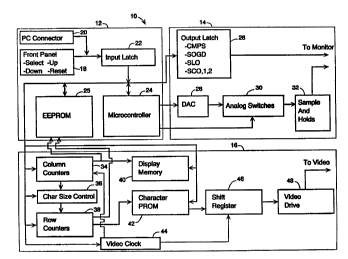
Figure 1 shows a block diagram of a video display adjustment and on-screen
menu
system in accordance with the present invention.
Figure 2 shows a circuit diagram of a video display adjustment and on-screen
menu
system in accordance with the present invention.
Figure 3 shows a circuit diagram of an analog switch and associated sample and
hold
circuits.
Figure 4 shows a circuit diagram of several analog switches and associated
sample
and hold circuits.
Figure 5 shows a flow chart of the operation of the present invention.
5
~~60396
DESCRIPTION OF THE PREFERRED EMBODY
In accordance with the present invention, FIG. 1 shows a schematic diagram of
the
video display adjustment and on-screen menu system 10 in accordance with the
present
invention. The system 10 comprises three principle functional blocks: an
input, memory
storage and controller block 12, a video display adjustment block 14 and a
character display
block 16. Within the input, memory storage and controller block 12, either a
front panel
18 or a PC connector 20 can be used to input adjustment selections to the
system 10. These
inputs are temporarily buffered in an input latch 22. A microcontroller 24
accepts these
inputs from the input latch 22, and stores changes to the video display
parameters in an
IO EEPROM memory storage area 25.
Within the video display adjustment block 14, certain display parameters
provided by
the microcontroller are buffered by an output latch 26. The majority of the
display
parameters are sequentially sent to a DAC 28 that converts the parameters to
analog signals.
These analog signals are demultiplexed by a series of analog switches 30
enabled after every
vertical sync pulse. The signals of each switch 30 are stored by a
complementary series of
sample-and-hold circuits 32. These circuits hold the parameters for display
operation until
new parameters are provided.
The third block, the character display block 16, generates and sends on-screen
menu
information to the video display synchronized to the display's horizontal
frequency. The
column counters 34 increment for each pixel being sent divided by the number
of pixels per
character. In the preferred embodiment, each character is 8 pixels across, so
the column
counters 34 divide the video clock signal by eight. When the column counters
34 reach their
end, the current line of the menu has been reached. A character size control
block 36 then
decides whether to repeat the current pixel line (essentially elongating a
character). Because
higher horizontal frequencies indicate an increased vertical resolution of the
display screen,
repeating individual character lines increases their vertical size. Characters
in the preferred
embodiment are created on an 8 by 8 grid, and then each pixel line is doubled,
to create an
6
~!~so3ss
8 by 16 displayed character. At higher frequencies, each pixel line of a
character is doubled
once more to create an 8 by 32 displayed character. Onto a set of repetitions
of a
character's pixel line are completed, the character size control block allows
the row counters
38 to increment to the next pixel line of the characters in the menu.
A display memory 40 holds the current array of character codes that make up
the
displayed menu. Every eight video clock ticks, the column counter 34
increments to indicate
the next character code in the current menu line. Every 16 (or if doubled, 32)
horizontal
sync pulses (scan lines), the row counters 38 increment the display memory 40
to the next
full Iine of character codes in the current menu. The current character code
(in ASCII)
IO pointed to in the display memory 40 by the column and row counters 34 and
38 refers to
character display information stored in a character PROM memory 42. Every
horizontal
sync pulse, the row counters 34 indicate which pixel line of the current
character display
information is read out of the character PROM 42. These pixel lines are
repeated 2 or 4
times depending on the horizontal frequency, as described. The pixel line for
each character
in the current embodiment is 8 pixels wide and is stored in a shift register
46, where it is
clocked out to a video drive 48. The video drive 48 blanks the current space
on the video
screen and replaces the video display with the current pixel line of character
display
information. A video clock 44 provides the appropriate video clock information
to the
column counters 34, the row counters 36 and the shift register 46 for
synchronizing the
output of each pixel of menu information.
FIGS. 2, 3 and 4 present circuit schematics of the present invention that
describe its
construction and operation in greater detail. FIG. 2 reveals most of the video
display
adjustment and on-screen menu system 10. The front panel 18 in the preferred
embodiment
comprises a series of switches having outpuu labeled Reset, Up, Down and
Select. Reset
resets all user adjustments to factory preset conditions, Select selects
adjustments from the
on-screen menu, Up increments an adjustment, and Down decrements an
adjustment. These
switch-provided inputs can be complemented by a series of direct inputs from a
PC
connector 20, allowing direct input to the menu system from an automated
factory adjustment
7
,~sp39s
system. The inputs are buffered by an input latch 22, comprising a 74LS3?3
octal
transparent Latch with 3-state outputs. The microcontroller 24 reads
information from the
input latch through its ports P0.1 through P0.7 whenever LATl is enabled. The
horizontal
sync (HS) and vertical sync (VS) signals are also sent through the input latch
22 to the
microcontroller 24, which determines whether they are present and their
polarities. If HS
and VS are not present then either SOG or a composite sync signal is used. The
HS signal
is sent to the INTO port of microcontroller 24 since its pulse width can be
too small to be
detected by the microcontroller 24 otherwise. The monitor can receive sync
information in
three ways: (a) separate horizontal and vertical sync signals; (b) a composite
sync signal
(where the horizontal and vertical sync are added together into one sync
signal); and (c) a
Sync On Green (SOG) signal, where the composite sync signal is added to the
GREEN
signal. The microcontroller 24 determines which of the three types of sync
signal is being
sent, then generates the SOG and CMPS signal to let the cozresponding circuits
know what
is being sent.
IS The microcontroller 24 preferably employs a 80C51 CMOS 8-bit CPU and a
l6MFiz
oscillator. In addition to controlling the on-screen menu system and the CRT
display
parameters, the microcontroller 24 creates the pin-cushion correction waveform
for the
display. A I6MHz oscillator was chosen to provide the necessary bandwidth to
synthesize
the waveform. The signals used throughout the invention as inputs and outputs
of the
microcontroller 24 have the following meanings: INTO is an external interrupt
activated by
a high-to-low transition of the vertical sync signal, that lets the
microcontroller 24 know
when to start generating the pin-cushion signal. Therefore, the preferred
embodiment uses
a negative vertical sync signal. The INTO input is also used to determine if
the monitor is
running synchronization on green and the horizontal sync HS. This alternative
procedure
occurs when the input latch 22 is enabled and the HS signal passes through to
INTO. An
inverter 49 is used to invert the VS signal and provide an open collector
output to share with
the input latch's HS output. The inverted signals HS' and VS' are always
positive going
horizontal and vertical synchronization pulses. INTl provides an output signal
WEEP* that
8
~Q60396
is the chip enable command for the EEPROM memory 25 when reading and writing
to the
EEPROM 25.
The TO input receives the HS' signal, allowing the microcontroller 24 to count
the
number of scan lines. The number of lines is used by the pin generation
algorithm, and also
to look up appropriate display parameters for a new horizontal frequency and
then output
these new parameters to the display. T1 provides the CRTD output signal that
is logical 1
when the on-xreen menu is enabled. Port P1.0-7 is an eight-bit data port that
outputs the
display parameter signals (including the pin-cushion waveform) to the DAC 28.
The RXD pin outputs a CLRL signal that clears the row counters 38. This method
is used for ease of programming and speed. There are only two dead periods
during the
display tracing where the pin-cushion waveform is not generated: during
vertical retrace and
in the center of the display. Two separate displays are shown during the on-
menu operations
of the present invention: a main menu, and a smaller Value Indicator Graph
(VIG) that
graphically represents the increments and decrements made by a user to a given
display
parameter (such as brightness). There is enough time in the center of the
trace to allow the
VIG to be erased and re-written to the screen while keeping the display
steady. When the
main menu is being displayed, however, there is not enough time even during
the center
portion of the trace. Therefore, the present invention rewrites the main menu
in two
complete trace cycles. First the menu is cleared from the SRAM display memory
area 40
in one cycle, and then is written in the next cycle, when the row counters 38
are also
cleared.
The TXD pin outputs the WRAM* signal which is the SRAM write enable signal,
for writing to the display memory 40. The ALE pin outputs the Address Latch
Enable
(ALE) signal which is the general read/write enable signal generated by the
microcontrollcr
24 for reading and writing all external RAM and ROM memories (such as FFPROM
25 and
display memory 40). The WR* signal is the write enable command generated by
the
9
~t~60396
microcontroller 24 for writing to cztcrnal RAM and ROM memories, while the RD*
signal
is the read enable command for reading these external memories.
LATO is used to control the output latch 25, LATl is used to control the input
latch
22. ASO*, AS1* and AS2* enable analog switches 0, I and 2 respectively (analog
switches
30A, B and C). The rest of port P2 (P2.0 through P2.2) along with port P0
(P0.0 through
P0.7) provides an 11-bit data and address bus DBO-10 for accessing external
RAM and ROM
through the invention. DBO-5 connect to the output latch 26 comprising a 74LS
I74 hex D
Flip-Flop integrated circuit. Output latch 26 stores several of the display
parameters that are
changed whenever a new video mode is present. The stored parameters of the
output latch
IO are changed by enabling LATO upon recognizing the new video mode, latching
the outputs
of PO.O-5 (via DBO-5) to the outputs of the output latch. The CMPS signal is 1
if no VS
signal is present, indicating a composite video signal. The SLO signal
controls the size of
the characters displayed. If SLO equals 0, each character has an 8 by 16 cell.
If SLO equals
1, the cell is 8 by 32. The SLO signal is sent to the character size control
block 36 discussed
further below.
Signals SCO-2 comprise a 3-bit signal indicating the horizontal frequency. If
the
signals SCO-2 equal 7, the frequency is 30khz, if the signals SCO-2 equal 0,
the frequency
is 75khz. All other values proportionately divide up the frequency spectrum
between these
two extremes. The SCO-2 values can then be used to switch in S capacitors for
different
frequencies to keep acceptable horizontal linearity of the display. The use of
S capacitors
for this purpose is well known to those skilled in the art.
The EEPROM chip 25 used in the preferred embodiment is an XL2815AP-250 that
is rated for a minimum of 10,000 writes per byte of memory. The FFPROM 25
stores all
the video display adjustment settings. ~ The chip select (V~EFP*), read enable
(RD*) and
write enable (WR*) are controlled by the microcontroller 24 as discussed
above. The
FFPROM chip 25 outputs DO-7 are sent to the PO port of the microcontrolles 24.
The
address lines for the EEPROM chip 25 come from the column and row counter
outputs COL
Z~60396
0 through COL 4 and ROW 0 through ROW 5. To minimize the number of separate
components, the present invention uses the column and row counters 34 and 38
also as
addrrss latches for addressing the EEPROM 25. The particular chips chosen for
the column
and mw counters 34, 38 (discussed below) are presettable, allowing them to
function as these
latches. First, DBO-10 loads the EEPROM readlwritc address into the column and
row
counters 34 and 38, enabled by the ALE signal. Then, the counters' outputs
address the
appropriate byte of EEPROM memory while DBO-7 reads or writes that byte's
data.
The digital-to-analog (DAC) block 28 receives its 8-bit digital signal from
port Pl of
microcontrollez 24, and converts the signal to analog form to provide to the
analog switches
IO 30 and their respective sample-and-hold circuits 32. The DAC 28 provides a
< 1 % linearity
with a linear change in digital input. While the schematic of Figure 2
illustrates the DAC
28 comprising discrete components, an appropriate integrated DAC can be
substituted. An
74LS05 hex inverter IC provides an open collector hex inverter since the P1
outputs of the
microcontroller 24 are not truly open collector and can cause non-linearities.
The
specifications of the particular components are as shown in FIG. 2. The output
VADJ of
the DAC 28 connects with three analog switches 30.
Referring now to figures 3 and 4, each analog switch 30 comgrise a CD4051B
single
8 channel analog multiplexer. The single DAC output VADJ drives the three
separate analog
switches 30 to provide 24 separate adjustments. Each respective analog switch
30A, B and
C is switched to on via signals ASO-2. Data bus lines DB8-10 then select 1 of
8 output lines
of the analog switch to enable. At the beginning of each vertical sweep, all
24 adjustments
are updated by sequentially turning on each analog switch and then, in turn,
that switch's
separate output lines SO-7, TO-7 and UO-7.
24 individual sample-and-hold circuits 32 are provided. Each circuit receives
one line
from a given analog switch 30. For example, switch 32g receives ~ signal S6
from analog
switch 30a. The signal S6 is turned on when ASO* is high, and DB8-10 reads
"110".
11
oso39s
Switch 32g provides the Focus adjustment for the display. All the switch
outputs,
connections and truth tables are provided below in Table 1.
Table 1.
Switch
Adjustment
Input
ASO*
AS1*
ASZ*
DB8
DB9
DB10
32a HPOS SO 1 0 0 0 0 0
32b HSIZE S 1 1. 0 0 0 0 1
32c VSIZE S2 1 0 0 0 1 0
32d VPOS S3 1 0 0 0 1 1
32e OSV S4 1 0 0 1 0 0
32f HSIZfi SS 1 0 0 1 0 1
32g FOCUS S6 1 0 0 1 1 0
32h G2 S7 1 0 0 1 1 1
32i n/a TO 0 1 0 0 0 0
32j PWR T1 0 1 0 0 0 1
IS 32k NV T2 0 1 0 0 1 0
321 DYNFOC T3 0 1 0 0 1 1
32m HHLD T4 0 1 0 1 0 0
32n HCTR TS 0 1 0 1 0 1
32o VHI.D T6 0 1 0 1 1 0
32p VLIN T7 0 1 0 1 1 1
32q RBIAS UO , 0 0 1 0 0 0
12
~oso39s
Switch
Adjustment
Input
ASO*
AS1*
AS2*
DB8
DB9
DB10
32r RGAIN Ul 0 0 1 0 0 1
32s GBIAS U2 0 0 1 0 1 0
32t GGAIN U3 0 0 1 0 1 1
32u BBIAS U4 0 0 1 1 0 0
32v BGAIN US 0 0 1 1 0 1
32w CONTRAST U6 0 0 1 1 1 0
32x BRIG~iT U7 0 ~ 0 ~ 1 1 1 1
Table 1 (contd.)
Each sample-and-hold (S/I-~ circuit 32 comprises an LM358 low-power op amp.
The
IO capacitors chosen for the S/H circuits 32 are 0.033 ~cfarads. Each S/H
circuit 32 is updated
for 6 ~csecs. every vertical sync pulse.
Referring back to Figure 2, the character display block 16 provides the on-
screen
menus and value indicator graphs for changing the display parameters. The
display of the
menus is regulated by the column and row counters 34 and 38. Column counters
34
IS preferably comprise chained 74F161 synchronous presettable binary counters.
The first three
output lines ADO-2 clock the eight pixels of each character pixel line and
latch data from the
character PROM 42 to the Shift Register 46. The higher-levci signal lines COLO-
COL4
address the display memory 40, indicating which character on the current menu
line is
active. The final output, RCO, indicates that the 32 columns of the menu line
have been
20 completed, and temporarily stops the video oscillator clock 44, until the
next horizontal sync
signal HS activates the clock again. The CLK signal for the counters is
generated by the
video oscillator clock 44. As noted above, the column and row counters 34 and
38 double
13
X960396
as address latches for reading and writing the EEPROM 25. During these
operations, the
ALE signal is substituted for the CLK signal.
The row counters 38 are also formed from chained 74LS161 synchronous
presettable
binary counters. The first 2 outputs of the row counters LNEl-2 are sent to
the character
PROM's second and third input bits, since each character has eight lines and
each line is at
least doubled (and sometimes quadrupled). LNEO (which attaches to the
character PROM's
first input, comes directly from the character size control block 36,
discussed further below.
The remaining output signals ROWO-5 address the display memory block 40,
determining
which row of character to display. Again, since the counters double as address
latches for
IO reading and writing the EEPROM 25, the data is latched using ALE instead of
the CLK
signal.
The charactez size control block 36 sits functionally between the column
counters 34
and the row counters 38. During menu display, as the columns for a given row
(of character
pixel line information) are exhausted, the character size control block
determines whether
IS to advance the row counters to the next row. In lower horizontal
frequencies, each line of
a character is doubled: i. e. , the column counters cycle through two complete
cycles of the
same character line before advancing the row counters. At higher frequencies,
when
characters would appear squashed, the character size control block 36 retards
the row
counter advance for four complete column cycles. The character size control
block 36
20 counts horizontal rows by using the HC* signal from the column counter
block 34, which
is the same as the horizontal sync signal HS.
The character size control block 36 preferably comprises a 74LS393 dual 4
stage
binary counter and a 74LS 151 8 input multiplexes, as indicated in FIG. 2. The
SLO signal
is sent by the output latch 26 and determines how many repetitions a row
should have. If
25 SLO = 0, the horizontal frequency signal HS is divided by 2, to obtain the
baseline 8 by 16
character cell. If SLO = 1, the HS signal is divided by 4, to obtain an
elongated 8 by 32
character cell. When no display is required, the ALE signal is substituted as
the row clock
14
~9~60396
so that address lines can be latched into the row counters 38 (when they
function as address
latches). The LCL signal line is the clock line for the row counters- Again,
the CLRL
signal from the microcontroller 24 clears the counters during the Vertical
Retrace, while the
CRTD* signal is the CRT display enable signal. The following Table 2 provides
the relation
between these signals.
CLRL SLO
CRTD* LCL
1 X 0 0
X X 1 AI F
0 0 0 HS/2
IO 0 ~ 1 0 ~ HS/4
Table 2.
The addresses generated by the column and row counters 34 and 38 are sent to
the
display memory block 40, comprising 2 1K by 4 static RAM 2114AL-2 chips. ROWO-
4 are
the row address Lines, allowing 32 possible menu rows to be stored, and COLO-4
are the
IS column address lines, allowing 32 characters per row. DBO-7 are the data
input lines from
the microcontroller 24 that can store characters for each address location.
Outputs DBO-5
connect to the character PROAi 42 to indicate which character to display,
while outputs DB6-
7 connect to the video drive 48 to cause appropriate video blattlang and color
for the menu.
As discussed above, the WRAM* signal is the write enable for the display
meraory SRAMs,
20 and the microcontroller WR* signal connects to each chip's CS* pin. The
WEEP* signal
is 0 if writing to the EEPROM 25, such that no writing is done to the display
memory 40.
In the preferred embodiment, although the system is capable of displaying 32
rows,
a maximum of 16 rows can be displayed before the VS signal clears the counter.
To assure
~~60396
that the display is always in the horizontal active area, only columns 8
through 24 are used.
Also, duo to speed limitations of the microcontrolles 24, only 5 rows are
used.
The character PROM memory block 42 comprises a 745472 512-by-8 byte TTL
PROM. Signals LNO-2 comprise the 3-bit character line address (providing 8
lines per
character) that comes from the row counters 38. Signals DBO-5 comprise the 6
bit character
address (allowing 64 possible characters) from the display memory block 40.
Data lines O1-
8 provide the character pixel line information (having 8 pixels per character
line) latched
from the character PROM memory block 42 to the shift register block 46 for
output to the
video display. DBO-5 determine which character to display, while LNO-2
determine which
IO line of that character to output. The character PROM 42 outputs the 8
pixels of the current
pixel line of the current character.
The video clock 44 provides the coordinating timing mechanism for the
character
display section 16. The clock 44 is a variable oscillator that is synchronized
to the incoming
horizontal frequency. The clock's frequency is controlled by varying an OSV
voltage
IS (determined by microcontroller 24 and stored by S/H circuit 32e) such that
character size is
kept fairly constant, regardless of horizontal frequency. The oscillator is
kept synchronous
to the horizontal frequency to maintain the menu information stationary on the
video display.
The video clock frequency is varied by controlling the constant current source
to the
oscillator by varying OSV. The clock is synchronized to the horizontal
frequency by gating
20 the horizontal sync signal HS with the oscillator, starting the oscillator
when each horizontal
line occurs. The clock is turned off when the columns for the display complete
their cycle
for one line. The OSV signal is an analog 10-15V signal stored by S/H circuit
32e. RCO
from counter U10 goes high when the counters reach FF (their end) and kills
the video clock
by using a 74LS393 as a latch. The horizontal sync signal HS' restarts the
clock by clearing
25 this 74LS393 latch. The output CLK drives the counters 34 and 38, while the
inverse output
CLK* drives shift register 46. Table 3 presents a truth table relating these
signals.
16
~so39s
CRTD * HS' RCO
~*
1 X X
0 1 X 0
0 p 0 Video Clock
0 0 1 0
Table 3.
The video clock 44 uses a 74F132 quad 2 input NAND Schmitt trigger, a 74LS02
Quad 2
input NOR gate, and other discrete components as indicated. The clock output
is between
IO and 20 Mhz dependent on incoming horizontal frequency. The clock's
frequency
preferably defaults to be proportional to the horizontal frequency. However,
the user can
also adjust the oscillator frequency for each mode by malting selections on
the menu, thereby
controlling the horizontal size of the characters.
The shift register 46 is a 74F166 8 bit shift parallel-to-serial register.
Data lines O1-
8 from the character PROM 42 provide the video information to the shift
register (the
IS current pixel line for the current character). The CLK* signal from the
video clock 44 shifts
the data to the output one bit at a time. ADO-2 are from the column counters
34 that latches
a new set of pixel information every 8 video clock ticks, loading the next
character's pixel
Line. Z is the video signal output sent to the video drive 48.
The video drive block 48 drives transistor amplifiers on the video display's
driver
circuitry. The video information normally sent to the video display is blanked
for an entire
character whenever character information is written to the display during menu
operation.
All other times, the normal video information is sent to the video display.
The video drive
block 48 employs three 74LS08 Quad 2 input AND gates. The Z lino is the video
signal
17
~9~60396
from the shift register, signal DB6 allows the Z signal to also drive the blue
video signal,
and signal DB7 is from the display memory block and blanks the PC's video for
1 character
cell The CRTD* signal is used to avoid false triggers: the system only blanks
a character
cell when this signal is active. RGD is the video signal drive for the red and
green video
signals. BD is the blue video signal, and BLANK blanks the RGB video signal
sent from
the computer that normally drives the display.
The sequential operation of the present invention is described in flow chart
50 of FIG.
5. Upon video display start-up, the initial conditions for the display are
read 52 by the
microcontmller 24 from the EEPROM memory 25 and sent via the DAC 28 and
digital
IO switches 30 to the individual sample-and-hold circuits 32. During every
vertical retrace, the
microcontroller 24 counts the number of horizontal Iines traced and determines
54 if the
number of lines differ from the previous count. If not, the microcontroller
asks 56 whether
the user has started to make any adjustments. If that is also not true, the
microcontroller
determines 58 if the reset button on the front panel 18 has been pressed. If
the answer is
IS also false, the microcontroller begins generating the top of the pincushion
waveform 60. If
any menu is being displayed, its contents are written 62 at the middle of the
display trace
to the display memory block 40. Then the microcontroller 24 generates the
bottom of the
pincushion waveform 64.
When the vertical sync interrupt occurs 66, the microcontroller 24 updates all
SIH
20 circuits 32, clears the menu display and counters 34, 38 and 40, and counts
the number of
horizontal lines again. If the line count is different, a different horizontal
frequency is being
used. The microcontroller 24 then determines 68 the horizontal frequency, the
vertical
frequency and the polarities of the signals. Having determined which new
frequency mode
is being used, the menu system then reads the appropriate display parameters
70 from the
25 EEPROM memory 25. These display parameters are then converted and sent 72
to the S/H
circuits 32, and the microcontroller 24 begins the normal operation' of
generating the
pincushion waveform in steps 60 through 66. If a user has begun changing any
adjustments;
as determined in step 56, the microcontroller 24 changes the appropriate
adjustmeat value,
18
~A~60396
both in the EEPROM memory 25, and at the next vertical retrace 66, the
appropriate S/H
circuit 32. If the user presses the Reset button at step 58, the
microcontroller 24 reads 74
the appropriate FFPROM memory for the factory-default staadards for the
current frequency
mode. Meanwhile, the normal operation of generating the pincushion waveform,
displaying
the menu display, and updating the S/H circuits 32 at the vertical sync signal
occur as before
in steps 60 through 66.
While the present invention has been described with reference to preferred
embodiments, those skilled in the art will recognize that various
modifications may be
provided. For example, any of the various electrical components can be
replaced by other
discrete or integrated circuitry having an equivalent function. Various menu
configurations
of columns and rows can be chosen depending on display requirements. Not all
the
discussed display parameters need to be included in the set addressed by the
on-screen meau
system, and others not described may be added. The exact order and timing of
various
circuit operations can be modified to correspond to different displays and
requirements.
IS These and othez variations upon and modifications to the described
embodiments are
provided for by the present invention, the scope of which is limited only by
the following
claims.
19