Note: Descriptions are shown in the official language in which they were submitted.
2060419
~ULTIPLE ADAPTER RESPONSE DETECTION CIRCUIT
Ba~k~round of t~e Invention
1. Field of the Invention
The field of the invention is industrial control systems
including programmable controllers, and more particularly,
communication links for connecting such controllers with
remote input and output circuits.
2. Background Art
Industrial control systems such as those described in
U.S. Patent Nos. 3,810,118, 3,942,158, 4,165,534 and
4,442,504 are typically connected to industrial equipmen,
such as assembly lines or machine tools to operate such
equipment in accordance with a stored program. The stored
program includes instructions which, when executed, examine
the condition of selected inputs to the system from sensir.
lS devices on the controlled equipment and energize or de-
energize selected outputs from the system to operate devices
on the controlled equipment.
Inputs to the system may be discrete binary signals s~
as those from switches which may detect limits of process
variables such as motion, temperature, time, or other
quantities, or the inputs may be analog measures of the
process variables themselves, which are generally then
converted to digital binary form for processing. Likew:s-,
the outputs of the system may be either binary outputs as
implemented by mechanical or solid-state relays, or ana --
outputs produced by means of a digital to analog conve~
2060~19
The inputs and outputs processed by the system are
received by the system through I/O modules. A number of I/O
modules may be placed with a programmable controller in a
rack containing a backplane which electrically interconnects
the I/O modules with the controller. Alternatively, the I~O
modules may be remotely located and connected to the
controller by means of a communications "link". An I/O
scanner incorporated into the controller allows the
controller to send and receive data on this link.
Remote I~O modules may be grouped together within a
remote rack having a backplane interconnecting the remote I~O
modules. This remote rack is then connected to the serial
link by means of an adapter. The adapter provides an
interface between the data on the link and the backplane of
the rack and provides a means for each I/O module to rece ~e
and transmit data on the link. Sixteen remote IJO racks ma~
be connected in "parallel" on the link, that is, connecte so
that each rack may monitor the link simultaneously.
The link connecting the controller and the adapters c-^
the remote I/O racks may take one of a number of topologies
One topology is that of a multidrop or "daisy chain"
configuration. In such a configuration, each adapter is
positioned along the link so that it is connected direct'~
with the controller and every other adapter. The adapte-s
are each given a unique address and messages are directed ~~
a particular adapter by transmitting the appropriate add-e~s
before the message.
A remote rack may hold 16, 12, 8, or 4 I/O moduies ~-_
therefore the address transmitted on the link before a
message includes a rack address and a starting quarte~
2060~19
permit multiple racks with less than 16 I/O modules to share
one rack address.
Orderly communication between the controller and the
remote adapters is ensured by having all communications on
the link initiated by the controller. If the controller
needs to transmit or "writen data to the remote I/O racks, it
transmits the data on the link and awaits the return of a
confirmation signal. If the controller needs to receive or
"read" data from the remote I/O rack, it transmits a data
request on the link and awaits the return of the data from
the remote I/O rack.
The address of each remote adapter is selected by the
user and entered by switches on each adapter. This user-
selected addressing permits maximum flexibility in
configuring the indust-ial controller and its remote IiO.
Remote I/O racks may be added or dropped as necessary and
their corresponding addresses reassigned to minimize changes
in the controller program.
This increased flexibility in configuring the indust ,al
control system as provided by user-selectable addressing,
carrie~ with it the risk of two remote I/O racks being
inadvertently assigned to the same address.
If duplicate addresses are assigned to two or more
adapters, data communicated on the link may be corrupted
the interference of those adapters transmitting to the `i-
~simultaneously. Such interference may also result from
multiple adapters responding to the same address as a res_:~
of adapter circuitry failure. Such multiple simultaneous
transmissions are termed "collisions".
2060419
Industrial control systems are sensitive to even a low
probability of collision even if the collisions may be
reliabiy detected. The link between the controller and the
remote I/O operates under severe real time constraints, and
periodic retransmission of garbled data caused by a collision
will unacceptably degrade the link's maximum response time.
Also, the possibility an undetected collision and thus of
undetected garbled data is a serious problem in the
industrial environment where expensive and complex machinery
is being controlled.
In some instances, a collision may cause electrical
damage to high powered output circuits on the adapters when
each attempts to take control of the link.
~ummary of the Invention
The present invention provides a method of unambiguousl-~
determining whether multiple adapters on a link are
responding to the same address. Specifically, an address
transmitted on the link is read by each of the adapters w~.:c:-
compare that address to its pre-assigned adapter address.
The link includes a conductor and if the address on the 1 -.c
matches the adapter address for a particular adapter, tha~
adapter generates an incremental current in the conducto-.
These incremental currents are combined to produce a tota
current related to the number of adapters so respondir.g.
This total current is compared to a predetermined thresho ~
to ensure that only a single adapter is responding.
It is a general object of the invention, therefore, ~
detect the presence of multiple adapters responding to a
single address and therefore to avoid meSQage collisior.s
might result in garbled data or damaged circuitry.
2060419
The current may be induced on the conductor by means of
a resistor having one end connected to a voltage source and
the other end connected to the conductor by a switch.
It is another object of the invention, therefore, to
provide a simple method of producing incremental currents on
the conductor which indicate the number of ~dapters
responding to an address, without the need for complex
circuitry.
The incremental currents on the conductor may be summed
across a resistor connected between the conductor and a
reference voltage, and the currents measured with a voltage
comparator responsive to the voltage across that resistor.
Accordingly, it is yet another ob~ect of the invention
to provide a simple method of measuring the combined
incremental currents on the conductor and thus to indicate
the number of adapters responding to an address.
The foregoing and other object~ and advantages of tr.e
invention will appear from the following description. I.. ~.e
description, reference is made to the accompanying drawi~,gs
which form a part hereof and in which there is shown by way
of illustration, a preferred embodiment of the invention.
Such embodiment does not necessarily represent the full sco~e
of the invention, however, and reference is made therefore ~_
the claims herein for interpreting the scope of the
invention.
2060~9
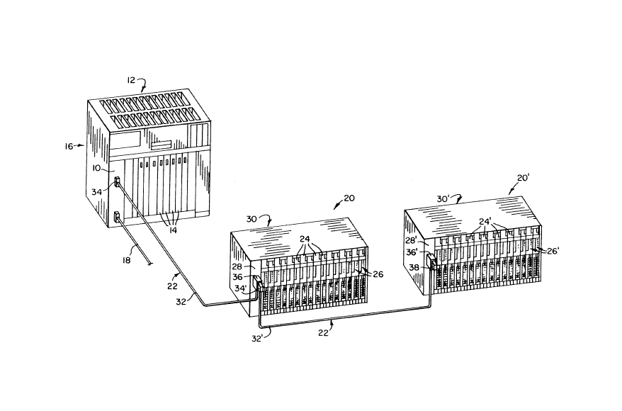
Fig~ 1 is a pictorial view of the communications iink o'
the present invention showing a controller and several remote
I~O adapters and racks arranged in daisy chain configuration;
Fig. 2 is simplified schematic representation of the
multiple adapter response detection circuitry of the
controller and of the two remote IJO adapters shown in Fig. 1
and also showing the MAR conductor of the link and its
termination resistor;
.Q Fig. 3 is a graph of the voltage range on the MAR
conductor of Fig. 2 showing the regions corresponding to
different numbers of responding adapters or the presence o-
absence of a termination resistor;
Fig. 4 and S are timing diagrams of read and write
cycles on the link between the controller and the adapters
showing the activation of the multiple adapter response
detectlon circuitry with relationship to the timing of the
other link signals; and
Fig. 6 is a detailed schematic of the multiple adapte
response circuitry of Fig. 2.
~ ipt;on of the Preferred Embod;ment
Referring to Figure 1, an industrial control system
employing the multiple adapter response (MAR) detection
circuitry of the present invention includes a programmab:e
controller 10 communicating through a backplane 12 with
adjacent I~O modules 14 within a rack 16. Additional -em~:e
I/O modules may be contained within one or more remote ~
racks ~not shown) connected to the psogrammable contro:` e- - '
~060419
via a serial remote I/O link 18. The programmable controller
10 sequentially addresses each remote l/O rack and the
~odules contained therein.
The remote I/O racks may be located up to 5000 feet from
the programmable controller 10. A programmable controller
with remotely located I/O racks is disclosed generally in
Markley et al. U.S. Pat No. 3,997,879, issued December 14,
1976 and entitled: ~Fault Processor for Programmable
Controller with Remote I/O Interface Racks."
The data throughput of the remote I/O link 18 is limited
by its serial format. This limit of data throughput may be
important for certain high speed I/O functions or when a
large number of remote I/O racks requires the scanning of
many I/O addresses.
The programmable controller 10 also communicates with a
number of local I/O racks 20 via a parallel local I/O link
22. The local I/O racks 20 are similar to the remote I~O
racks, having up to 128 I/O circuits arranged in I/O mod~J~es
24 held in as many as sixteen slots 26. The local I/O racKs
20 connect to the parallel local I/O link 22 through an
adapter 28 held in a separate slot 26 and communicating w~:s
the I/0 modules 24 over a backplane 30 on the rear of the
rack 20.
The local I/O link employs a 50 conductor cable 32
having conductors arranged in 25 twisted pairs and conr.ecte-
to the programmable controller 10 by a standard male S0
D-type connector 34. The other end of the cable 32 is
attached to the adapter 28 of a first local I/O rack 2C ~.
one connector, a two headed connector 36. The two heade~.
connector is constructed of two standard male 50-pin D-
~
2060419
_onnectors wired in parallel. The connectors are held?hysically in a single shell so that they face in opposite
directions with their mating axes parallel to each other ts
present an inner and outer facing connector. The uncommitted
S outer connector of the two headed connector 36 may be
attached to a second cable 32' similar to the first. One end
of this second cable 32', fitted with a single male 50-pin D-
type connector 34', is attached to the outer connector of the
two-headed connector 36, and the second end of the second
cable 32~, fitted with a two-headed connector 36' is attached
to an adapter 28' of a second local I/O rack 20'. This
connection system, termed "daisy chainingn, may be repeated
for multiple local I/O racks 20, each of which then has
direct and simultaneous access to the local I/O link 22.
The connectors on the ends of the cables 32 and 32'
having single connectors 34 and 34', are mechanically
attached to their matinq connectors on programmable
controller 10 or on two-headed connector 36 or 36' by mear.s
of engaging, spring-loaded hooks as are known in the art. ~-.
contrast, the two-headed connectors 36, 36' are attached to
their mating connectors on the adapters 28 and 28' by mea..s
of captive machine screws (not shown) that are threaded ir.s
threaded bored holes in the mating connectors. The ca?t~e
machine screws are positioned so that they may be removed
from the threaded holes thus disengaging the two-headed
connecters 36 and 36' f-om the adapters 28 and 28', wi~
disturbing either the connections between the outer conn.e~
of the two-headed connector 36 and the connector 24', o-
between the two-headed connecter 36' and the terminati~~
38. Thus, any local I/O rack may be removed from the !~
2060419
without disturbing the integrity of the communications on the
link 22 between the other adapters 28 (28') on local I/O
racks 20 (20') and the programmable controller 10.
The outer uncommitted connector of the last two-headed
connector 36' receives a terminating unit 38 mating with the
outer uncommitted connector of the two-headed connector 36'
to shunt certain of the twisted pairs of the cable 32' with
terminating resistances (not shown in Fig. 1) to prevent the
reflection of signal enerqy at the end of the cable 32' as is
understood in the art. The mechanical attachment of the
cables 32 and 32', as described, preserves the linear nature
of the daisy chaining and prevents "star" type configurations
with cables radiating out from a single common connection
point. Specifically, there are no bored holes in the
controller 10 for receiving the two-headed connector's
machine screws. This ensurss that the link 22 may be
reliably terminated with a single termination unit 38.
As mentioned the local I/O link 22 employs a 50
conductor cable 32, 32' ~o permit parallel transmission c
data and the higher data transmission rate commensurate
this format. Table I summarizes the function of each
conductor in the cables 32 and 32'.
2060419
Table I
.conduc or nunber dec~a~at;o~
l-32 data/address
33,34 parity
35,36 mode line
37,38 address strobe
39,40 read strobe
41,42 write strobe
43,44 data transfer acknwldg.
45,46 bus error
47 MAR power
48 MAR
49 MAR return
MAR ground
Data and addresses communicated between the programmable
controller 10 and the local I/O adapters 28 and 28' are
multiplexed onto the first 16 twisted pairs of the cable 32,
32' ~conductors 1-32). ~hese twisted pairs are driven
differentially, as is understood in the art, to improve r.o~se
immunity. The 17th twisted pair (conductor 33 and 34)
provides a parity bit for these first sixteen pairs.
Conductors 35 through 46 are combined in differentia:'i
driven twisted pairs to provide six control lines: mode,
address strobe ~"AS"), read strobe (nRSn), write strobe
("WS~), cable data transfer acknowledge (nC~TACK") and ca_:e
bus error ("CBERR"), as w ll be discussed further below~
The remaining four conductors are used in the mult~e:-
adapter response (~MAR~) detection circuitry of the inve~.~ ~~
and include: MAR power ("PWR"), MAR ground ("GND"), the `~
--10--
2060419
'ine (nMAR") ~ and the MAR return ~"RTNn); (collectively the
"M~R Lines"), as will also be described further below.
~.eneral De~cr~ption of the M~R C;rcuit~y
Referring to Figure 2, the MAR lines connect a MAR
detection circuit on the programmable controller 10
("controller MAR circuit 40" ) and to MAR detection circuits
on one or more local I/O adapters 28, 28' ("adapter MAR
circuits 41, 41'"). As described above, the cable 32, 32' is
daisy chained between the programmable controller 10 and the
local I/O adapters 28, 28' so that each adapter MAR circu ts
41, is attached in parallel with other adapter MAR circui s
41' along the link 22.
The PWR line 42 is connected, at the controller MAR
circuit 40, to a positive voltage source 52 and communicates
that voltage 52 to the adapter MAR circuits 41 and 41'.
Likewise the GND line 50 connects the adapter MAR circuits Y
and 41' to a ground reference 54 at the controller MAR
circuit 40.
Within the controller MAR circuit 40, the MAR line 44
and the RTN line 48 are connected through a resistor 56, a.~i
the MAR line 44 is connected to the input of comparator
circuitry 59 which evaluates the voltaqe across the resiste-
56. Also within the controller MAR circuit 40, the RT~ 2-.~
GND lines 48 and 50 are connected together so that the ~.`;
line 48 is at ground potential.
The MAR and return lines 44 and 48, like all the
conductors of the cable 32, 32' connect to each of the
I/O adapters 28, 28'. After the last zdapter 28, the ~
RTN lines 44 and 48 are shunted by a termination resis~-- C
2060~19
Each of the adapter MAR circuits 41 and 41' includes a
-esistor 58, (58') with one end attached to the PWR line 42
and one end connected through series, normally-open switch B
(B') to the MAR line 44.
S Within the MAR detection circuit 40, a resistor 60 with
one end attached the PWR line 42 is connected through a
series, normally open switch A to the M~R line 4~.
~p~rat; o~ of the M~R c; rcuit
I. Detection of Mu.tiple Adapter Responses
Referring to Figs. 2 and 3, the voltage on the MAR line
44 is limited to the range between the voltages of the PWR
and GND lines 42 and S0.
During a period of no link activity, each of switches B
and B' are open. Accordingly, the voltage across resisto~ r 6
is in ~egion I (shown in Fig. 3) near ground as a result o~
the parallel connection of resistor 56 and terminating
resistor C acro~s the MAR line 44 and the RTN line 48, the
latter which is at ground potential.
When a particular adapter 28 or 28' is addressed by ..~e
programmable controller 10 via the link 22, the switch B
associated with that adapter 28 is closed as will be
described further below. If only one such adapter 28
responds to the given address, as is proper, the voltage ~.~
the MAR line 44 will increase and rise into Region II o' -:_
3 as determined generally by the resistive divider forme~ -
resistor 58 in series with the parallel combination of
resistors 56 and C, this resistive divider operating, ~e~-e~
PWR and GND lines.
2060419
In the event that two adapters 28 and 28' respond to the
address issued by the programmable controller 10 over the
link 22, either though the same address being assigned by the
user to both adapters 28 and 28' or a decoding circuit
failure, then two or more resistors 58 and 58' will be
connected in parallel between the PWR line 42 and the MAR
line 44 forming a new resistive divider with the parallel
combination of resistor 56 and C, to ground, and the voltage
on the MAR line 44 across resistor 56 will rise into Region
10 III as shown in Fig. 3.
The comparator circuit 59 employs a high threshold 62
and low threshold 64 to distinguish between these three
Regions I, II, and III and to generate two digital signals D
and ~ having a high and low state which indicate to the
programmable controller 10 into which Region the voltage Gf
the MAR line 44 falls and thus whether none, one, or more
than one adapter MAR circuit is responding.
If the low threshold 64 is exceeded, line D goes high
indicating the number of adapter is greater than or equal tO
one. If the high threshold 62 is exceeded, line Y goes hig~.
indicating that the number of adaptors is greater than '.
Thus, the combination of these signals positively identir es
whether the proper number of adapters, i.e. one, is
responding.
206~9
I'. Detection of Improper Termination
The proper termination of cable 32 improves the
integrity of the link 22 and is also necessary for the above
described detection of multiple adapter responses. If the
termination resistor C is missing or of improper value, the
voltages on the MAR line 44 will differ from their proper
values for the various numbers of adapter responses as shown
in Fig. 3. For this reason, the presence of a termination
resistor C is first determined by the controller MAR circuit
40.
Prior to activity on link 22, typically when the
programmable controller 10 is first activated, switch A in
the controller MAR circuit 40 is closed. The value of the
resistance 60 connected to this switch A is the same as the
value of resistors 58 and 58' and hence closing switch A
raises the voltage on the MAR line 54 to Region II, as if one
adapter were responding only.if the termination resistor C is
in place. If the termination resistor C is missing or too
high ln value, the voltage on the MAR line 44 will rise into
the Region III indicating improper termination. Converse ~,
if the termination resistor ~ is present but too low in
value, the voltage on the MAR line 44 will not rise to Reg_o-
II but will remain in Region I also indicating improper
termination.
These conditions are summarized in the following ta~ e
in which a "1" indicates a closed switch, a proper
termination, or a digital "true" state, and in which a "~'
indicates an open switch, a missing termination, or a d~
-14-
2060~19
"false" state depending on the column as will be apparent
from con~ext:
Table II
~ a ~ s~a~a
1 0 0 1 Region II 1 0 test-termination OK
1 0 0 0 Region III 1 1 test-termination high
0 0 0 1 ~egion I 0 0 no response
0 l 0 1 Region II 1 0 one response
0 1 1 1 Region III 1 1 two or more responses
S ~
Referring to Figs. 1 and 4, switch B in each of the
adapter MAR circuits 41, 41' is realized by means of a PNP
transistor 62 with its emitter connected to the PWR line 42
and its collector connected to the resistor 58 which in tur~,
connects to the MAR line 44. A signal 64 at the base of
transistor 62 with a voltage approximately equal to that of
the PWR line 42 holds the transistor 62 off or the switch B
open. The switch B iS closed when the voltage of the base
signal 6g drops below the voltage of the PWR line 42. The
base signal 64 to the transistor 62 is generated by
communication circuitry 33 in the adapter 28 as will be
described below.
Switch ~ in the controller MAR circuit 40 is constructe~
identically to that of switch B in the adapter MAR circui~ ~l
including a PNP transistor 66 with its emitter connected ~-
the PWR line 42 and its collector connected to the resis~_-
60 which in turn connects to the MAR line 44. A base si~
68 to the transistor 65 is generated by communication
20604~9
circuitry 31 associated with the programmable controlle- 10
in response to link 22 activity as will be described below.
Resistor 56 is connected to ground through a N-channel
MOSFET 70 which permits it to be deactivated when the
programmable controller 10 deactivated in a stand-by mode as
is useful in certain redundant configurations. During the
MAR detection process, the FET 70 is always in the conducting
state.
Resistor networks 72 in conjunction with comparators 74
and 76 establish the threshold voltages 62 and 64 of Fig. 3.
First, the power supply voltage 52 is precisely regulated by
series resistor 78 joining the cathode of zener diode 80,
whose anode is connected to ground. The regulated voltage a
the ~unction of resistor 78 and zener diode 80 is divided by
1~ two resistive dividers formed of series resistors 82 and 84
to ground and series resistors 86 and 88 to ground which
produce regulated threshold voltages 90 and 92 equal
respectively to the low and high threshold voltages 64 and 62
respectively. Capacitor 94 to ground from the junction of
resistor 78 and zener diode 80 to ground and capacitors 96
and 98 shunting voltages signals 90 and 92 to ground
respectively, serve to decouple these voltages fro~. power
supply variation as is known in the art.
Voltage signal 90 is connected to the inverting inpu 5'
comparator 74 which receives the MAR line 44 at its non-
inverting input. The output D of the comparator 74 is hiyh~
therefore, only when the MAR line 44 exceeds the voltage 9
or the threshold voltage 64. This output D generally
indicates that one or ~ore adapters 28, 28' are respor.d~
the programmable controller 10.
-16-
2060~19
Voltage signal 92 is connected to the inverting input of
comparator 76 which also receives the MAR line 44 at its non-
inverting input. The output ~ of the comparator is high,
therefore, only when the MAR line 44 exceeds the voltage 92
or the threshold voltage 62. This output ~ generally
indicates that more than one adapter 28, 28' is responding to
the programmable controller 10. The two outputs D and ~
together, therefore, serve to establish whether none, one, or
more than one adapter 28, 28' is responding to the
programmable controller 10 as has been described above.
These outputs D and L, are received by the programmable
controller 10 as will be described.
Referring for the moment to Fig. 1 and Table 1, the
adapters 28, 28' of the local I/O racks 20, 20' include we!l
lS understood communications circuitry 33 that handle the
routine protocol of the link 22 includinq monitoring the
address, data and control lines of the link 22 and triggeriny
the appropriate responses by the adapter 28, 28'. The
communicationq clrcuiery may comprise generally a dedicated
microprocessor in combination with link driving circuitry,
such as in known in the art, or may be a custom integrated
circuit embodying a state-machine for response to link
protocols and communicating with the I~O modules 24 and 2~,'
directly.
Likewise, the link protocol at the programmable
controller 10 is handled by similar communications circu~
31. These communications circuits free the programmable
controller 10 and the adapters 28, 28l of the local /O -~ ~s
20, 20' from the computational overhead of monitoring a^._
timing various link signals and allow the link protocc! - .-e
2060~19
invisible with respect to the programmable controller 10 and
the adapters 28, 28' of the local I~O racks 20, 20'. Such
communications circuits 31 and 33 are well known in the art.
Certain timing signals used in the communications protocol of
the link 22, and decoded by the communication circuitry 31
and 33, are available to the controller 10 and adapter MAR
circuits 40 and 41 and control the timing of the MAR circuits
40 and 41 as will now be described.
The general timing diagram of a read and write cycle on
the parallel link 22 is shown in Fig. 5 and 6 and will be
familiar to those of ordinary skill in the art. Referring
first to Fig. S, the programmable controller 10 may initiate
a read cycle, during which data 106 may be, for example,
transferred from the local I/O rack 20 to the programmable
controller 10, by transmittinq on the A/D lines of the lir.k
22, the address 100 of the local I/O module 24 of interest.
The status of this transmitted data a~ an address 100 is
indicated by the presence of the address strobe signal 102 on
the AS line which also serves to indicate that A/D lines have
had time to settle into a valid state, taking into account
various internal propagation delays. The programmable
controller 10 then issues a read signal 104 on the RS line.
The adapter 28 communications circuitry 33 compares this
address 100 against its own address, set by the user, and if
they match, upon the occurrence of the read signal 104,
solicits the desired data 106 from the respective I/O modu:es
24 and transmits it to the programmable controller 10 v~a ~.e
A/D lines. As is well understood in the art, the A/D li-.e~
are tri-state to permit bi-directional communication be~~ee^
the programmable controller 10 and the local I~O adapte~s
-18-
2060419
Shortly after the address strobe 102, the control
circuitry of the adapter 28 also activates the switch B to
connect resistor 58 to the MAR line 44 which rises in
voltage, as described, above depending on the number of other
adapters 2B' responding, to create a MAR signal 109.
The transmission of the data 106 is accompanyed by a
data acknowledge signal 108 on the CDTACK line. If instead
the CBERR line is asserted or if the controller MAR circuit
40 indicates that more or less than one adapter 28, 28' is
responding to the particular address 100, then the
communication circuitry 31 of the programmable controller lO
informs the programmable controller 10 of the exact nature of
the error.
Referring now to Fig. 6, the programmable controller 10
may also initiate a write cycle, during which data 110 may
be, for example, transferred to the local I/O adapter 28 f-o...
the programmable controller 10. The address 100 of the
destination I/O module 24 is asserted on the A/D line and ~.e
address strobe signal 102 provided on the AS line as before.
The programmable controller 10 then asserts the data 110 to
be written, on the A/D lines, and issues a write strobe ':2
on the WS line.
The adapter 28 communications circuitry 33 compares ~:~e
address 100 against its own address, set by the user, ar.d
they match, activates the adapter MAR circuit 41 closing
switch B creating a MAR signal 109. Upon the occurrence ~-
the write strobe 112, the adapter 28 receives the writte-.
data 110 and if the data error free asserts the CDTAC~ :^.e
to create a data transfer acknowledge signal 108. Con~e-^-
-19-
2060~19
if the parity of the data is wrong, a bus error signal 108'
is asserted on the CBERR line.
The voltage of the MAR line 44 during these transactio.s
is monitored by the control circuitry 31 of the progra~mable
controller 10 and if the voltage of the MAR slgnal 109
indicates the presence of more or le~ than one adaptor 28,
28' responding to the particular address 100, then the
control circuitry 31 of the programmable controller 10
informs the programmable controller 10 of the exact nature of
the error via communication channels therebetween.
A preferred embodiment of the invention has been
described, but it should be apparent to those skilled in t~.e
art that many variations can be made without departing f-~m
the spirit of the invention. For example, the current
generated on the MAR line 44 could be of either polarity a-.d
could be generated by other means than resistors so long ~s
each adapter may generate a current increment that may
combine to indlcate the total number of adapters genera~ n~
such current increments. Clearly this MAR detection circ~
may be readily expanded to more than one remote adapter.
-20-