Note: Descriptions are shown in the official language in which they were submitted.
2060617
NEW AND IMPl?OVED THERMAL INKJET
PRINTHEAD ORIFICE PLATE AND
NETHOD OF MANUFACTURE
Technical Field
This invention relates generally to the manufacture o~
orifice plates for inkjet pens and more particularly to the
fabrication of such orifice plates having an increased
thickness and an orifice opening convergent geometry to
improve print quality performance.
Backaround Art
In the manufacture of thin film printheads for thermal
inkjet pens, it has been a common practice to align and bond
a metal orifice plate to an ad~acent thin film resistor
substrate using an adhesive barrier insulating material such
as VacrelT~ sold by the DuPont Company of Wilmington, Delaware.
It has also been a common practice to photolithographically
define a plurality of ink firing chambers and ink feed
channels in the VacrelT~ layer so that each firing chamber
therein is aligned with respect to each heater resistor on an
underlying thin film resistor substrate and to an orifice
opening or group of openings in the ad~acent orifice plate.
In this manner, the heater resistors may be electrically
driven as is well known to heat the ink within each of the
firing chambers to boiling and thus cause the ink to be
ejected from the orifice openings in the orifice plate and
onto an ad~acent print medium.
In the past, it has been a common practice to use
electroforming processes to electroplate the orifice plate
member into a desired geometry before being transported to an
orifice plate attachment station. At this location these
orifice or nozzle plates are first optically aligned with the
thin film resi~tor substrate and barrier layer thereon and
then adhesively bonded to the Vacrel~ barrier layer so that
the orifice openings in the electroformed orifice plate are
precisely aligned with respect to the heater resistors on the
Ca8e 189183
2060617
thin film resistor substrate. Various types o~ electroforming
processes have been used in the past in the ~ormation o~ these
orifice plates and are disclosed, for example, in U. S. Patent
No. 4,773,971 issued to Si Ty Lam et al, in U. s. Patent No.
4,675,083 issued to James G. Bearss et al and in U. S. Patent
No. 4,694,308 issued to C. S. Chan et al. All of these above
identified patents are assigned to the present assignee and
are incorporated herein by reference.
It has also been a common practice to electroplate
these orifice plates on a metal surface and up and over the
edges of insulating regions or islands on the metal surface so
as to form orifice openings having contours which converge
toward the surfaces of these insulating regions or islands.
These orifice openings normally converge from a large orifice
opening at the back of the orifice plate and smoothly into a
smaller orifice opening at the front or ink ejection surface
of the orifice plate. As is also well known, the preference
for using a convergent geometry orifice opening of this type
in the fabrication of thermal inkjet printheads is to minimize
"gulping~ within the orifice plate and adjacent ink firing
chambers and thereby in turn reduce cavitation wear on the
thermal inkjet printhead heater resistors during the firing of
the ink;et pen. A further and more detailed discussion of
this problem of gulping and cavitation wear on the heater
resistors may be found in the above commonly assigned U.S.
Patent No. 4,694,308 issued to C. S. Chan et al.
Various types of orifice plate alignment and thin film
resistor substrate attachment processes and procedures are
also disclosed generally in the a~ove referenced patents and
are disclosed in more process-related detail describing the
overall thin film printhead fabrication technigues and
printhead architecture in the Hewlett Packard Journal, Volume
16, No. 5, published May 1985, and also in the Hewlett Packard
Journal, Volume 39, No. 4, published August 1988, both
incorporated herein by reference.
Case 189183
2060617
The orifice plate fabrication process being currently
used by the present assignee i8 disclosed in the above
identified U. S. Patent No. 4,773,971 is~ued to Si Ty Lam et
al and also in a copending application Serial No. 07/236,890
of Si Ty Lam et al which is a continuation application of U.
S. Patent No. 4,773,971. This issued patent and continuation
application of Si Ty Lam et al both disclose electroplating
processes for forming thermal inkjet printhead orifice plates
wherein various metals are electroformed on selected
substrates. These selected substrates or mandrels are grouped
into one class comprising selected metal patterns formed on an
underlying insulating layer or substrate and in another class
comprising selected insulating patterns formed on an
underlying metal layer or substrate. Of particular interest
in these Lam et al electroforming processes for making these
precision architecture orifice plates is an orifice plate
fabrication process wherein a durable inorganic dielectric
pattern such as silicon carbide, SiC, is formed on an
underlying layer of stainless steel which in turn is supported
by a thick glass or guartz plate.
Whereas the above orifice plates produced by the
electroforming processes disclosed in the above identified
U. S. Patent No. 4,~73,971 and copending application Serial
No. 07/236,890 of Si Ty Lam et al have proven to be highly
regarded and commercially succe~sful and superior in mo~t
aspects of their operational performance, and whereas these Si
Ty Lam electroforming processes are capable of producing high
precision architecture orifice plates with closely controlled
orifice diameters and center-to-center orifice spacings, there
are neverthele~s certain applications where it is desired to
increa~Q the thickness of these orifice plates in order to
increa~e the thickness of the orifice bores therein. This
reguirement is necessary in certain applications in order to
decrea~e the ink drop spray which is sometimes caused when the
"tail" of an e~ected drop of ink i8 swept against one side of
a convergent orifice opening as the ink drop is ejected from
Case 189183
2060617
the outer or ink ejection orifice surface of a thermal inkjet
thin film re~istor-type printhead. Thi~ ink spraying e~ect
is particularly evident in thermal ink;et printhead designs
and architectures wherein the heater resistors of the thin
film resistor substrate are offset slightly with respect to
the orifice opening center line. This heater resistor offset
is used in order to compensate for directionality errors which
will otherwise occur when the heater resistors are precisely
aligned with respect to these orifice opening center lines.
This ink drop spray effect in turn produces a visible edge
roughness where the ink drop or dot is deposited on an
adjacent print medium, and this edge roughness in turn
degrades the resolution and print quality of the printed
media.
Disclosure of Invention
The general purpose and principal object of the present
invention is to provide a new and improved thermal inkjet
orifice plate architecture and method of manufacture wherein
these orifice plates are operative to provide a significant
improvement in print quality performance and resolution of the
inkjet printed media.
Another ob;ect of this invention is to minimize and
substantially eliminate the above problem of ink drop spray
and thereby in turn minimize and substantially eliminate
visible edge roughness of dots printed on an adjacent printed
media.
Another object of this invention is to provide a new
and improved orifice plate fabrication process useful in the
manufacture of thermal inkjet printheads which utilizes
existing technologies to produce orifice plates and associated
printhead structures which are reliable in operation and which
may be economically manufactured at relatively high yields.
A feature of this invention is the provision of a new
and improved orifice plate of the type described whose
thickness has been significantly increased relative to prior
Case 189183
2060617
art orifice plate desiqns while simultaneously maintaining
good smooth convergence in the geometry of the ori~ice
openings developed in the orifice plate.
Another feature of this invention is the provision of
a new and improved orifice plate of the type described wherein
good smooth convergent orifice opening geometries are achieved
by electroforming stacked multiple metal layers on a removable
and reusable mandrel and having aligned convergent orifice
openings in each of the adjacent metal layers which together
define composite convergent orifice openings in the completed
orifice plate structure.
Another feature of this invention is the provision of
a new and improved thermal inkjet orifice plate of the type
described wherein the good smooth convergent orifice opening
geometry is achieved in a different method by the use of
anisotropic plating of the orifice plate on an underlying
substrate or mandrel. Using this method, the orifice plate
thickness or vertical plating occurs at a higher rate than its
lateral plating to thereby maintain good smooth convergent
geometries at the orifice openings therein.
Another feature of this invention is the provision of
a new and improved orifice plate fabrication process of the
type described wherein enhanced orifice plate thickness is
achieved by the fabrication of a metal layer-insulating layer
composite structure. In this novel structure, the insulating
layer i5 multi-functional in purpose in that it not only
provides an integral part of the completed orifice plate thus
formed, but it further serves as a permanent mandrel used in
the electroplating of the metal layer portion of the composite
orifice plate.
In a first, multiple layer electroforming process
embodiment according to the present invention, the above
ob~ects and related advantages are achieved by the steps of:
a. providing a mandrel having a surface area thereon
comprised of conductive and insulating regions,
Case 189183
206~617
b. electroforming a first metal layer on the mandrel
surface area and on the conductive regions thereon and
extending over the edges of the insulating regions of the
mandrel to form convergent orifice openings therein located on
top of the insulating regions,
c. forming an insulating pattern on top of the first
metal layer so that insulating sections or islands within the
insulating pattern overlie and are approximately laterally
coextensive with the insulating regions of the mandrel, and
d. electroforming a second metal layer on top of the
first metal layer and extending over the edges of the
insulating section or islands of the insulating pattern to
form convergent orifice openings within the second metal layer
which are aligned with the convergent orifice openings in the
first metal layer, whereby the aligned convergent orifice
openings in the first and second metal layers preserve and
form an overall orifice opening convergent contour extending
from an outer surface of the first metal layer to an outer
surface of the second metal layer.
In a second, anisotropic plating embodiment of this
invention, the above objects and related advantages are
achieved by the steps of:
a. providing a mandrel having a surface area thereon
comprised of conductive and insulating regions,
b. electroplating a metal layer on the conductive
regions of the mandrel and over the edges of the insulating
regions thereon to thereby form convergent orifice openings
atop the in~ulating regions, and
c. anisotropically plating the metal layer at a
vertical or layer thickness rate which is greater than the
plating rate in the lateral direction perpendicular to the
vertical or thickness dimension, whereby metal orifice plate
layer thicknessea on the order of 75 micrometers or qreater
are achieved simultaneously with the production of convergent
orifice opening geometries.
Case 189183
. ~ .
. ' .
- .
2060617
In a third embodiment of the present invention, the
above objects and related advantages are achieved by the steps
of:
a. providing an insulating substrate having a metal
pattern thereon,
b. electroplating a metal over the surfaces of the
metal pattern and into contact with an exposed ~urface of the
insulating substrate to form convergent orifice openings in
the electroplated metal layer, and
c. creating openings in the insulating substrate
which are aligned with the convergent orifice openings in the
metal orifice plate layer to thereby extend the opening
convergence and contour of the metal orifice plate layer fro~
one side of the insulating substrate to the other, whereby
the insulating substrate and ad~acent metal orifice plate
layer form a composite metal-insulator orifice plate structure
capable of being formed to a total thickness on the order of
75 micrometers or greater.
The above brief summary of the invention, together with
its various objects, features, and attendant advantages will
become better understood with reference to the following
description of the accompanying drawings.
8rief Descrimtion of the Drawinas
Figures lA through lE are a series of abbreviated
schematic cross-sectional views illustrating the sequence of
proces~ steps used in a first embodiment of the invention.
Figures 2A and 2B are abbreviated schematic cross-
section view~ illustrating a second embodiment of the
invention wherein anisotropic plating is utilized to form the
novel metal orifice plate described herein.
Figures 3A, 3B and 3C are abbreviated schematic cross-
section views illustrating a third embodiment of the invention
wherein a composite metal layer-insulating layer orifice plate
structure is formed using the insulating layer as a permanent
Case 189183
,................. .
2060617
mandrel and integral part of the composite orifice plate
structure thus formed.
Although only a single convergent orifice plate opening
is shown in Figures 2A and 2B and in Figures 3A through 3C, it
is to be understood that these openings are merely
representative of a larger plurality of orifice openings which
may be arranged in any desired geometry, such as in circular
primitives, angled rows and columns and the like.
Detailed Description of the Preferred Embodiment
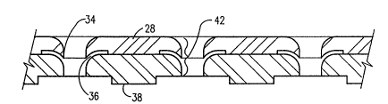
Referring now to Figure lA, there is shown a reusable
mandrel which is designated generally as 10 and includes a
main supporting substrate 12 which will typically be either a
glass or quartz plate having a thickness on the order of 90-
120 mils and having a thin layer 14 of sputtered stainlesssteel deposited on the upper surface thereof. A surface
pattern 16 of a selected inorganic dielectric material such as
silicon carbide, SiC, is formed as shown as an electroplating
mask on the upper surface of the stainless steel layer 14 and
thus in effect forms a three layered reusable mandrel
structure upon which the first electroplating step is carried
out to form a first orifice plate layer 18 in accordance with
the present invention as described below.
Referring now to Figure lB, the mandrel 10 is
transferred to an electroforming station where a selected
metal such as nickel is electroplated in the geometry shown to
form a first orifice plate layer 18 having a plurality of
convergent orifice or nozzle openings 20 therein which are
defined by electroplating the nickel up and over the edges 22
of the plurality of inorganic insulating islands or regions
16. The first nickel layer 18 will typically be plated to a
thickness on the order of about 50 micrometers.
Referring now to Figure lC, a suitable insulating
pattern 24 such as photoresist is formed in the geometry shown
with the photoresist islands 24 being positioned and centrally
aligned in the orifice openings 20 in the layer 18 and
Case 189183
2060~17
extending up and over the convergent edges 26 of the first
electroplated nickel layer 18. These photoresist islands 24
are approximately laterally coextensive with the lateral
dimensions of the silicon carbide insulating islands 16
disposed on the stainless steel surface layer 14 as previously
described. The photoresist islands 24 will typically be about
2 micrometers in thickness and will be of either the same
lateral dimension or either slightly greater or slightly
smaller than the lateral dimension the silicon carbide discs
16.
Referring now to Figure lD, the structure shown in
Figure lC is transferred to an electroforming or
electroplating station wherein a second metal layer 28, also
of nickel, is electroplated on top of the first metal layer 18
and up and over the outer edges of the photoresist pattern 24.
The second layer 28 of electroplated nickel also has a
convergent contour 30 at the orifice openings thus formed, and
these convergent orifice openings extend down into a point of
contact 32 with the photoresist islands 24. If desired, the
process illustrated in Figure lD herein may be further
extended to include three electroplated layers (not shown)
rather than the two layers shown in the figures.
Referring now to Figure lE, the double layer plated
structure shown in Figure lD is transferred to a suitable soak
solvent etching station wherein the photoresist pattern 24 is
removed to leave the "bird beak" geometry 34 as shown and
having the recessed cavities 36 which extend upwardly in the
contour as shown between the first and second electroplated
layers 18 and 28 of nickel. The second layer 28 of nickel
will typically be plated to a thickness of between 30 and S0
micrometers to thereby extend the total thickness of the
composite orifice plate structure shown therein to a thickness
of between 80 and 100 micrometers. The composite orifice
plate structure shown in Figure lE has been further treated to
remove the mandrel 10 including the glass substrate 12, the
stainless steel sputtered layer 14, and the lower silicon
Case 189183
2060617
11
carbide islands 40 from the lower surface 38 o~ the structure.
This composite orifice plate shown in Figure lE has the
desired overall convergent orifice contour indicated generally
by reference number 42, and with the small orifice diameters
typically on the order of 20-50 micrometers and with orifice
center-to-center spacings typically on the order of 80-180
micrometers.
Thermal inkjet pens have been built using the orifice
plate structure shown in Figure lE, and the print quality of
the print sample generated by such pens was excellent. These
samples exhibited a negligible amount of edge roughness as a
result of the undesirable ink spray which has previously been
observed in the use of the prior art pens described above.
Referring now to Figures 2A and 2B, there is shown a
second embodiment of the present invention wherein anisotropic
electroplating is used as an alternative embodiment to the
metal layer stacking process described above with reference to
Figures lA through lE. In Figure 2A, there is shown a glass
plate or substrate 44 upon which a surface layer 46 of
stainless steel has been sputtered deposited. A mask pattern
48 of a selected inorganic dielectric material such as silicon
carbide has been deposited as shown on the surface of the
stainless steel layer 46 using known masking and inorganic
materials deposition techniques. The composite reusable
mandrel consisting of glass, steel and inorganic dielectric
materials 44, 46, and 48 is then transferred to an anisotropic
plating station wherein a thick layer 50 of nickel is plated
up and over the edges 52 of the silicon carbide discs or
island~ 48.
The electroplating rate in the vertical or thickness
dimension of the metal plate 50 may be made to be
signi~icantly greater than the electroplating rate in the
lateral or width dimension of the orifice plate 50. This
technique is useful to generate the convergent orifice bore
geometry in the orifice plates being fabricated. One
technique which has been proposed to accomplish this
Case 189183
2060~17
12
anisotropic electroplating is to first dilute the
electroplating solution to about six (6) ounces per gallon o~
total nickel content and to reduce the electroplating current
to a level which is sufficiently low to avoid burning. Then,
a water soluble polymer such as a high molecular weight
polyvinyl alcohol or a polyethylene glycol should ~e added to
the electroplating solution so that it is operative to reduce
the diffusion of nickel ions substantially to the upper
surface areas of the metal being plated and minimize the
electroplating rate in the orifice bores.
Another suitable Watts Nickel solution which has been
proposed for this anisotropic plating would include the use of
dilute nickel sulfate, NiSo4 6H2O, of twenty-two (22) ounce~
per gallon of electroplating bath; nickel chloride, NiCl6 in
twelve ounces per gallon of electroplating bath and six (6)
ounces of boric acid per gallon of electroplating bath. Then,
by agitating the solution this has the effect of supplying
more nickel ions to the top surfaces of the nickel being
electroplated and simultaneously it reduces the nickel ion
concentration in the orifice bore region. The current
density, agitation rate and electroplating temperature may be
varied by those skilled in the art to arrive at a desired or
optimum vertical-to-lateral nickel electroplating rate for
ultimately producing the desired embodiment as shown in Figure
2B.
The solution temperature should be set somewhere in the
range of 35-40C. Using this process, an orifice plate 50 may
be expected to plate up to a thickness of about 75 micrometers
or greater while simultaneously maintaining the integrity of
the smooth convergent contour 54 of the orifice openings thus
iormed which terminate at a point of contact 56 on the
surfaces of the silicon carbide islands 48.
Once the electroplating process used to form the nickel
layer 50 has been completed, the reusable mandrel consisting
of layers 44, 46, and 48 is peeled away from the lower surface
58 of the nickel layer 50 to thereby leave the orifice plate
Case 189183
2060617
13
50 intact and ready for transfer to an orifice plate alignment
and attachment station for securing the orifice plate to a
thin film heater resistor substrate and barrier layer (not
shown). If greater orifice plate thicknesses are desired,
additional layers of metal may be electroplated as described
above with reference to Figures lA-lE.
Referring in sequence now to Figures 3A, 3B, and 3C
there is shown in Figure 3A a permanent mandrel which is
identified generally as 60 and includes a polyimide or other
suitable substrate material 62 which is formed to a thickness
typically on the order of about 25 micrometers. A metal
pattern 64 having a plurality of openings 66 therein is
deposited on the upper surface of the polyimide substrate 62,
and the metal pattern 64 will typically be a material such as
copper deposited to a thickness of approximately a 1000
angstroms and with openings of 20-50 micrometers in diameter
and center-to-center spacings of 80-180 micrometers. The
permanent mandrel 60 shown in Figure 3A is transferred to an
electroplating deposition station wherein a thick metal layer
68 such as nickel is plated in the convergent geometry shown
in Figure 3B on the top of the copper pattern 64 and down over
the edges 66 thereof and into a point of contact 70 with the
upper surface of the polyimide substrate layer 62.
The composite orifice plate structure shown in Figure
3B is then transferred to another materials processing station
where the polyimide material in the region 72 of the layer 62
and bounded by the sidewall boundaries 74 is removed such as
by the use of a laser ablating process. One such process is
described in an article by Poulin and Eisele entitled
"Advances in Excimer Laser Haterials ProcessingU, ~EI~
,P~oceeding,s, Volume 998, page 84, Lumonocs Press, September
1988. This step further extends the orifice bore dimension
and convergent contour of the previously formed orifice
openings 76 in the metal layer 68 down along the aligned
sidewalls 74 of the opening 72 in the polyimide material 62.
In this manner, the output ink ejection orifice opening of the
Case 189183
, ... .
2060617
14
thus formed structure is now located at the circular exit
opening or hole 78 in the polyimide layer 62. The polyimide
layer 62 will typically be on the order of about 25
micrometers in thickness, whereas the metal electroplated
layer 68 will typically be on the order of about 50
micrometers in thickness to bring the total composite layer
thickness of the orifice plate structure shown in Figure 3C to
a value on the order of 75 micrometers or greater.
The provision of a composite orifice plate of the type
described and having an outer polyimide layer as shown in
Figure 3C has several attendant advantages. First, the
polyimide orifice plate material has a non-wetting surface
which impedes the build-up of ink thereon, thus impeding ink
spray and providing repeatable drop trajectories. Secondly,
the interior surfaces of the polyimide materials may be
rendered wettable by the use of laser ablation, thereby
enhancing orifice refill and bubble purging characteristics
while impeding bubble ingestion and enhancing the high
frequency stable operation of the orifice plate. Thirdly, the
polyimide material provides for the ease of manufacturability
as a result of its reel-to-reel processing capability.
Various modifications may be made in and to the above
described embodiments without departing from the spirit and
scope of this invention. For example, the invention described
above is not limited to either the particular metals used in
the mandrels described or those metals used in the formation
of the electroplated metal orifice plates. Reusable mandrels
compri~ing metal substrates having selected insulating
pattern~ formed thereon such as those described in the above
identified U. S. Patent No. 4,773,971 and application Serial
No. 07/236,890 to Si Ty Lam et al may be used instead of the
specifically described metal-on-insulator mandrels in the
above three embodiments of the invention. In addition, the
nickel orifice plates described above may be further treated
3S such as by the use of gold plating techniques to plate the
surfaces of the metal orifice layers with gold after the
Case 189183
2060617
orifice or nozzle plate structures have been completed as
described. Also, if greater orifice plate thicknesses are
required for any of the above described embodiments,
additional layers of metal may be electroplated as described
above with reference to Figures lA-lE.
Accordingly, the above and other design and process
modifications available to those skilled in the art are within
the scope of the following appended claims.
Case 189183
.......... .