Note: Descriptions are shown in the official language in which they were submitted.
~~'~w1~; _D3
.e 10 '~
SPECIFICATION
BACKGROUND Of' THE INVENTION
1. Field of the Invention
This invention relates to a diamond-coated hard material having a diamond-
or diamond-like carbon-coating layer with a high bonding strength to a sub-
strate.
2. Description of the Prior Art
Diamond having many excellent properties, for example, very high hardness,
chemical stability, high heat conductivity, high sound wave propagation speed,
etc. has widely been used as hard materials utilizing these properties or dia-
mond or diamond-like carbon coated hard materials, illustrative of which are
as follows:
OO single crystal diamond, sintered diamonds or diamond-coated cutting
tools such as throwaway inserts, drills, microdrills, endmills, etc., which
are capable of cutting Al, Cu, various practically used light metals or alloys
thereof at a high temperature and obtaining well finished surfaces, because of
hardly reacting with these metals or alloys.
O various wear resistance tools such as bonding tools capable of work-
ing for a long time with a high dimensional precision, because of high wear
resistance.
O various machine parts such as radiating plates.
~ various vibration plates such as speakers.
O various electronic parts.
In the production of artificial diamond, there are methods of forming dia-
mond coating layers from gaseous phase, for example, microwave plasma CVD
method, RF-plasma CVD method, EA-CVD method, induction field microwave plasma
CVD method, RF hot plasma CVD nethod, DC plasma CVD method, DC plasma jet meth-
od, filament hot CVD method, combustion method and like. These methods are
useful for the production of diamond-coated hard materials.
Since many of the diamond-coated hard materials are lacking in bonding
- 1 -
I I
CA 02060823 2002-04-02
strength of the diamond-coated layer to a substrate, the diamond-coated layer
is stripped to shorten the life in many cases. The great reason therefor is
that diamond not capable of forming intermediate layers with all materials has
low wettability with other materials.
In order to obtain a diamond-coated hard material having a high bonding
strength, there have been proposed a method comprising selecting a substrate
having the same heat expansion coefficient as diamond (Japanese Patent laid-
Open Publication No. 291493/1986, proposing sintered Compacts containing
Si,N~ as a predominant component, and sintered compacts containing SiC as a
pre-
dominant component), a method comprising subjecting the surface of a substrate
to etching to remove metals having bad infueneces upon formation of the
diamond
coating layer on the substrate surface and thereby increasing the formation
den-
sity of diamond nuclei on the substrate surface (Japanese Patent Laid-Open Pub-
lication No. 201475/1989, etching the surface of a cemented carbide with an
acid solution to remove Co metal component and to suppress graphitization of
the diamond nuclei; Japanese Patent Laid-Open Publication No. 124573/1986,
subjecting the surface of a substrate to a scratching treatment with diamond
grains or a diamond wheel and thereby improving the nuclei forming density on
the surface of the substrate), etc.
As described above, diamond is chemically stable and does not form inter-
mediate compounds with all materials. When a diamond-coated hard material hav-
ing an excellent bonding strength is prepared, therefore, such a condition
must
be provided that a diamond coating layer and a substrate are bonded by a
strong
physical strength.
The inventors have made studies to realize this condition and consequently,
have found that when protrusions having a high bonding strength to a substrate
are formed on the surface of the substrate by a chemical or mechanical means
and a diamond coating layer is formed thereon, thereby forming such a state
that protrusions are intruded into the diamond coating layer, the bonding
strength between the diamond coating layer and the substrate is rendered very
- 2 -
CA 02060823 2002-04-02
high. This can be considered to be due to that the contact area of the diamond
coating layer with the substrate is increased and the protrusions have anchor
action in the diamond coating layer, whereby the diamond coating layer is hard
to be stripped from the substrate.
SUMMARY OF THE INVENTION
It is an object of the present invention to provide a diamond-coated hard
material having an excellent bonding strength, whereby the above described
problems can be solved.
The above described object can be attained by:
(I) a coated hard material comprising a diamond- and/or diamond-like
carbon-coating layer formed on the surface of a hard material, i.e. substrate,
characterized in Chat (1) microscopic roughness is present on the surface of
the substrate and (2) protrusive parts thereof are defined by the surface
roughness Rmax within a range of 1.0 to 30 a m in a standard length when the
standard length is 50 a m in the interface of the diamond- and/or diamond-like
carbon coated layer and the substrate, and (II) a coated hard material compris-
ing a diamond- and/or diamond-like carbon-coating layer formed on the surface
of
a hard material, i.e. substrate, characterized in that (1) microscopic rough-
ness is present on the surface of the substrate. (2) at least one protrusive
part is present in a standard length when the standard length is 10 a m in the
interface of the diamond- and/or diamond-like carbon coated layer and the sub-
strate, (3) the ratio of sum A of the lengths of dent parts to sum B of the
lengths of the protrusions is in the range of 0.05 ~ A/B ~ 20 in the standard
length in the interface and (4) the protrusions are intruded into the diamond-
coated layer.
BRIEF DESCRIPTION OF THE DRAWINGS
Fig. 1 is a schematic view of a coating layer-substrate interface in one
embodiment of the present invention.
Fig. 2 is a schematic view to illustrate the state shown in Fig. 1 by
linearly drawing it.
- 3 -
fir, "~ ~ rt.~'3
Fig. 3 is a schematic view of a coating layer-substrate interface in
another embodiment of the present invention.
DETAILED DESCRIPTION OF THE INVENTION
In the present invention, the roughness is not macroscopic roughness
formed by a scratching treatment with (1) a diamond wheel or (2) diamond grind-
ing grains, but microscopic roughness in a very small range, i.e. roughness in
a standard length of 50 a m or 10 a m in a diamond coating layer-substrate
interface..
The inventors have made various roughened states and consequently, have
found that when the surface roughness in the substrate interface is defined
by Rmax of 1.0 to 30 a m in the standard length of 50 a m and the pro-
trusive parts are intruded by at least 0.2 a m into the diamond coating layer-
substrate interface, a strong bonding strength is obtained. This surface
roughness is defined as a surface roughness (Rmax) of a substrate after coated
by lapping a cross-section of the substrate coated with diamond, observing and
photographing to review a boundary line of the diamond coating layer-substrate
interface. This corresponds to the above described invention (I).
The inventors have made various roughened states and consequently, have
found that when at least one protrusive part is present in the standard length
of 10 a m and the ratio of sum A of the lengths of dent parts to sum B of the
lengths of the protrusions is in the range of 0.05 s A/B s 20 in the standard
length and the protrusions are intruded by 0.2 a m into the diamond-coated
layer, a high density strength is obtained. This is calculated by lapping a
cross-section of the substrate coated with diamond, observing and photograph-
ing to review and model a boundary line of the diamond coating layer-substrate
interface. This corresponds to the above described invention (II).
In the present invention, it is preferable to carry out the commonly used
scratching treatment of a substrate with diamond grains in order to promote
formation of diamond nuclei on the whole surface of the substrate at the
initial
period of coating. During the same time, this scratching treatment is more
- 4 -
. i
CA 02060823 2002-04-02
preferably carried out by adding the substrate and diamond grains to a solvent
such as water, ethyl alcohol, acetone, etc. and then applying ultrasonic vaave
thereto, since a scratching treatment by pressing hard diamond grains against
the substrate in phyiscal manner results in breakage of the resulting protru-
sions. Diamond nuclei are uniformly formed on the whole protrusive and non-
protrusive parts of the substrate surface by this scratching treatment,
whereby
it is rendered possible to form such a state that the protrusions are intruded
into the diamond coated layer.
As a useful method for forming the specified roughness on a substrate,
there are m a method comprising depositing columnar or hexagonal pillar
crystal
grains and/or needle crystal grains on the surface of a substrate, 4 a method
comprising removing an etchable binder by etching, (~? a method comprising
mask-
ing a substrate, etching and then removing the mask, O a method comprising
physically working, for example, by appllying laser and the like. Depending
on the kind ofthe substrate, a suitable method should be chosen therefrom.
The method D consists in subjecting a substrate to some heat treatment,
freely growing columnar or hexagonal pillar crystal grains or needle crystal
grains and/or promoting secondary crystal generation on the surface thereof by
the substrate component, the method ~ is available for a material composed of
a hard phase and a binder phase, differing in corrosive property against acids
and alkalies, and is more available in the case of using a hard phase
previously
being in a columnar or hexagonal pillar or needle form and the method~ con-
sists in providing a mask in a suitable pattern using a photomask, etching
and then removing the mask by etching.
As a material for forming the protrusion, there can be used silicon car-
bide, silicon carbide-containing materials, tungsten, tungsten carbides or
carbonitrides, carbides or carbonitrides of tungsten with at least one metal,
titanium nitrides. carbides, carbonitrides or solid solutions thereof or mix-
tures thereof and materials containing them.
The material for forming the roughened part is preferably consolidated in
- 5 -
i i
CA 02060823 2002-04-02
one body with the substrate and is preferably a same material as that of tl~e
substrate. Of course, similar materials but differing in composition can be
used.
In Fig. 1, the state of the diamond-coated layer- or diamond-like carbon-
coated layer-substrate interface according to the present invention (I) is
schematically shown. That is, a macroscopic undulation appears in the inter-
layer, but Rmax is calculated regarding this undulation as linear as shown in
Fig. 2.
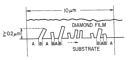
In Fig. 3, the state of the diamond-coated layer- or diamond-like carbon-
coated layer-substrate interface according to the present invention (II) is
schematically shown. Herein, the ratio of sum A of the protrusion lengths,
i.e. ~ A to sum B of the dint lengths, i.e. E B must be in the range of
0.05 ~ E A / E B ~ 20 and the intruded lengths of the protrusions are
preferably at least 0.2 a m. For example, when one protrusion of 0.5 a m is
present in 10 a m, ~ A / E B = 19.
In the present invention (I), the formed protrusive parts should satisfy
the requirements that when a standard length is 50 a m in the interface of a
diamond- and/or diamond-like carbon coated layer and a substrate, the surface
roughness of the substrate interface is represented by an Rmax of 1.0 to 30 a
m
in the standard length and the protrusive parts are preferably intruded in the
diamond coated layer with at least 0.2 a m. When the surface roughness at the
substrate interface is represented by a Rmax of less than 1.0 a m, the bonding
strength is not increased, while if more than 30 a m, on the contrary, the
bonding strength is lowered. When the maximum intrusive depth of the protru-
sions is at most 0.2u m, the bonding strength is substantially similar to
that in the case of providing no protrusion.
In the present invention (II), it is required that when the standard
length is 10u m in the diamond- and/or diamond-like carbon coated layer-sub-
strate interface, at least one protrusion is formed in this standard length,
the ratio of sum B of the lengths of protrusions and sum A of the lengths of
-6-
ii
CA 02060823 2002-04-02
the protrusions is in the range of 0.05 to 20 and the protrusions ace intruded
into the diamond-coated layer. In this case, the intruded length is preferably
at least 0.2 a m. When the ratio of sum B of the lengths of protrusions and
sum
A of the lengths of the protrusions is outside the range of 0.05 ~ E A / E t3
~ 20, the bonding strength Is not improved.
As the substrate, any hard materials can be used, for example, cemented
carbides, cermets, A120~, silicon carbide and other ceramics. Above all, when
protrusions of titanium compounds such as titanium carbides, nitrides and
carbonitrides and/or titanium compounds-containing materials, tungsten
carbides
and/or carbides of tungsten alloys and/or materials containing these compounds
or materials are present, a high bonding strength can be obtained. Further-
more, when the shape of the protrusion is a Columnar or hexagonal pillar
crystal
or needle crystal with an aspect ratio of at least 1.5, a bonding strength is
further increased.
As to the thickness of the diamond coated layer, if less than 0.1 a m, no
improvement of various properties by the coated layer, such as wear
resistance,
is found, while if more than 200 a m, further improvement of the properties
cannot be given. Therefore, a thickness of 0.1 to 200 a m is preferable.
The foregoing illustration is conducted as to a case where diamond is
coated, but the present invention can be applied with similar benefits to
cases
where diamond-like carbon is present in a diamond-coated layer, one or more of
these layers are coated and the coated layer contains foreign atoms such as
boron, nitrogen, etc. Where diamond-like carbon Is coated, the excellent ad-
vantages of the present invention can also be obtained.
The following examples are given in order to illustrate the present in-
vention in detail without limiting the same.
Example 1
A throwaway insert comprising silicon carbide whiskers ceramic (specific-
ally. AltOa-35 vol % SiC whiskers-5 wt % ZrO,) as a substrate and having a
shape
of SPG 422 was made, brought into contact with fused NaOH and etched to expose
- 7 -
CA 02060823 2002-04-02
needle crystals of silicon carbide whiskers having a minor axis of 1 a m and
a major axis of 8 a m on the surface of the insert. This insert and 2 g of
diamond grains each having a grain diameter of 8 to 16 a m were added to
ethyl alcohol, to which supersonic wave vibration was added for 15 minutes.
Using 2.45 GHz microwave plasma CVD apparatus, the thus resulting insert was
heated at 1000°C and maintained in a mixed plasma of hydrogen-2 %
methane at a
total pressure of 80 Torr for 8 hours to prepare a cutting insert coated
with diamond of 8 a m in layer thickness.
For comparison, a comparative insert was prepared by using a substrate
having the same shape and composition as described above without conducting
the
etching treatment and providing a diamond coated layer on the insert having no
needle crystals of silicon carbide whiskers on the surface thereof (The ultra-
sonic wave treatment was not carried out for the comparative sample).
In this test, it was confirmed by the Raman spectrometry that the coated
layer deposited on the surface of the substrate was a diamond coated layer.
Using these cutting inserts, intermittent cutting tests were carried out
under the following conditions.
trorkpiece to be cut: Al-24 wt % Si alloy (block material)
Cutting Speed . 400 m/min
Feed . 0.1 mm/rev
Cutting Depth . 0.5 mm
When the flank wear width, the wear state of the edge and the deposition
state of the workpiece, after 3 and 10 minutes, were observed, the cutting in-
sert of the present invention showed normal wearing represented by a flank
wear
width of 0.05 mm after 10 minutes from start of cutting and deposition of the
workpieCe was hardly observed. On the other hand, in observation of the cutt-
ing edge after 3 minutes from start of cutting, a large peeling of the diamond
coated layer was found, the flank wear width amounted to 0.16 mm and the work-
piece was subject to marked metal deposition, so that the cutting had to be
stopped.
_ g _
~r a ~r.~..
When the insert after the cutting test was cut, subjected to lapping and
then the interface of the substrate and diamond coated layer was observed by
an optical microscope, the insert of the present invention gave the results
that silicon carbide whiskers were intruded into the diamond-coated layer by
at most 3.5 a m and in the interface, the microscopic surface roughness was
represented by an Rmax of 4 to 5 a m in the standard length of 50 a m. In
the comparative insert, on the contrary, there were found no silicon carbide
whiskers in the interface of the substrate and diamond-coated layer, nor
intrusion of the substrate into the diamond-coated layer.
Example 2
A throwaway insert comprising JIS-K10 cemented carbides (specifically,
WC-5 % Co) as a substrate and having a shape of SPG 422 was prepared,
subjected
to mirror working and then to laser working, whereby to obtain inserts (1) and
(2) of the present invention worked in:
(1) lattice of grooves each having a depth of 3.0 a m and a width of 1.5
a m at an interval of 2 a m and
(2) lattice of grooves each having a depth of 6.0 a m and a width of 3.0
a m at an interval of 3 a m.
The resulting samples had respectively a microscopic Rmax of 3 and 6 a m as
calculated values.
In the similar manner to described above, this insert and 2 g of diamond
grains each having a grain diameter of 8 to 16 a m were added to ethyl
alcohol,
to which supersonic wave vibration was added for 15 minutes. On the surface of
the thus prepared insert was formed a diamond-coated layer with a thickness of
6 a m by the use of a known hot filament CVD method under the following con-
ditions:
Reaction Tube Vessel . Quartz Tube of 200 mm in Diameter
Filament Material . Metallic W
Filament Temperature . 2400 °C
Distance between Filament and
- 9 -
Insert Surface . 7.0 mm
Total Pressure . 100 Torr
Atmospheric Gas . HZ-1.5 % CHa Gas
Time . 7 hours
For comparison, a comparative insert was prepared by using a substrate
having the same shape and composition as described above without conducting
the
laser treatment and providing a diamond coated layer on the insert (The ultra-
sonic wave treatment was not carried out for the comparative sample).
In this test, it was confirmed by the Raman spectrometry that the coated
layer deposited on the surface of the substrate was a diamond coated layer.
Using these cutting inserts, intermittent cutting tests were carried out
under the following conditions.
Workpiece to be cut: A1-12 wt % Si alloy (round rod)
Cutting Speed . 1000 m/min
Feed . 0.15 mm/rev
Cutting Depth . 1.5 mm
When the flank wear width, the wear state of the edge and the deposition
state of the workpiece, after 5 and 30 minutes, were observed, the cutting in-
serts (1) and (2) of the present invention showed normal wearing represented
by
a flank wear width of 0.02 mm or 0.03 mm after 10 minutes from start of
cutting
and deposition of the workpiece was hardly observed. On the other hand, in
observation of the cutting edge after 5 minutes from start of cutting, a large
peeling of the diamond coated layer was found, the flank wear width amounted
to 0.24 mm and the workpiece was subject to marked metal deposition, so that
the cutting had to be stopped.
When each of the inserts after the cutting test was cut, subjected to lapp-
ing and then the interface of the substrate and diamond coated layer was ob-
served by an optical microscope, the insert of the present invention gave the
results that the cemented carbide as a substrate was intruded into the diamond-
coated layer by at most 3 a m and in the interface, the microscopic surface
- 1 0 -
ii
CA 02060823 2002-04-02
rough ness was represented by an Rmax of 2.8 or 6.1u m in the standard length
of 50 a m, which was confirmed to be substantially the same as the value meas-
ured before the coating. In the comparative insert, on the contrary, there
were found no intrusion of the substrate into the diamond-coated layer, nor
presence of the roughness.
Example 3
A throwaway insert comprising silicon carbide whiskers ceramic (specific-
ally, AIZOa-35 vol % SiC whiskers-5 wt % ZrOx) as a substrate and having a
shape
of SPG 422 was made, brought into contact with fused NaOH and etched to expose
needle crystals of silicon carbide whiskers having a minor axis of 1 a m and
a major axis of 8 a m on the surface of the insert. This insert and 2 g of
diamond grains each having a grain diameter of 8 to 16 a m were added to
ethyl alcohol, to which supersonic wave vibration was added for 15 minutes.
Using 2.45 GHz microwave plasma CVD apparatus, the thus resulting insert was
heated at 1000°C and maintained in a mixed plasma of hydrogen-2 %
methane at a
total pressure of 80 Torr for ? hours to prepare a cutting insert coated
with diamond of 9 a m in layer thickness.
For comparison, a comparative insert was prepared by using a substrate
having the same shape and composition as described above without conducting
the
etching treatment and providing a diamond coated layer on the insert having no
needle crystals of silicon carbide whiskers on the surface thereof (The ultra-
sonic wave treatment was not carried out for the comparative sample).
In this test, it was confirmed by the Raman spectrometry that the coated
layer deposited on the surface of the substrate was a diamond coated layer.
Using these cutting inserts, intermittent cutting tests were carried out
under the following conditions.
Workpiece to be cut: A1-24 wt % Si alloy (block material)
Cutting Speed . 400 m/min
Feed . 0.1 mm/rev
Cutting Depth . 0.5 mm
- 1 1 -
iC~'~ ~ ~.~ T : ~"i. T
When the flank wear width, the wear state of the edge and the deposition
state of the workpiece, after 3 and 10 minutes, were observed, the cutting in-
sert of the present invention showed normal wearing represented by a flank
<aear
width of 0.05 mm after 10 minutes from start of cutting and deposition of the
workpiece was hardly observed. On the other hand, in observation of the cutt-
ing edge after 3 minutes from start of cutting, a large peeling of the diamond
coated layer was found, the flank wear width amounted to 0.14 mm and the saork-
piece was subject to marked metal deposition, so that the cutting had to be
stopped.
When the insert after the cutting test was cut, subjected to lapping and
then the interface of the substrate and diamond coated layer was observed by
an optical microscope, the insert of the present invention gave the results
that silicon carbide whiskers were intruded into the diamond-coated layer by
at most 4 a m and in the interface, 3 to 6 protrusions were present and A/a
was 1.0 to 1.6 in the standard length of 10 a m. In the comparative insert,
on the contrary, there were found no silicon carbide whiskers in the interface
of the substrate and diamond-coated layer, nor intrusion of the substrate into
the diamond-coated layer.
Example 4
A throwaway insert comprising JIS-K10 cemented carbides (specifically,
wC-5 ~ Co) as a substrate and having a shape of SPG 422 was prepared,
subjected
to mirror working and then to laser working, whereby to obtain inserts (1) and
(4) of the present invention worked in:
(1) lattice of grooves each having a depth of 3.0 a m and a width of 1.5
a m at an interval of 2 a m and
(2) lattice of grooves each having a depth of 3.0 a m and a width of 3.0
a m at an interval of 3 a m.
(3) lattice of grooves each having a depth of 0.2 a m and a width of 1.5
a m at an interval of 2 a m and
(4) lattice of grooves each having a depth of 3.0 a m and a width of 2.0
- 1 2 -
II'. I
CA 02060823 2002-04-02
a m at an interval of 8 a m.
The resulting samples had respectively a A/B ratio of 1.75, 1.33 and 0.25.
In the similar manner to described above, this insert and 2 g of diamond
grains each having a grain diameter of 8 to 16 a m were added to ethyl
alcohol,
to which supersonic wave vibration was added for 15 minutes. On the surface of
the thus prepared insert was formed a diamond-coated layer with a thickness of
6 a m by the use of a known hot filament CVD method under the following con-
ditions:
Reaction Tube Vessel . Quartz Tube of 200 mm in Diameter
Filament Material . Metallic W
Filament Temperature . 2400 °C
Distance between Filament and
Insert Surface . 7.0 mm
Total Pressure . 100 Torr
Atmospheric Gas . H2-1.5 % CH, Gas
Time . 7 hours
For comparison, a comparative insert was prepared by using a substrate
having the same shape and composition as described above without conducting
the
laser treatment and providing a diamond coated layer on the insert (The ultra-
sonic wave treatment was not carried out for the comparative sample).
In this test, it was confirmed by the Raman spectrometry that the coated
layer deposited on the surface of the substrate was a diamond coated layer.
Using these cutting inserts, intermittent cutting tests were carried out
under the following conditions.
Workpiece to be cut: A1-12 wt % Si alloy (round rod)
Cutting Speed . 1000 mlmin
Feed . 0.15 mm/rev
Cutting Depth . 1.5 mm
When the flank wear width, the wear state of the edge and the deposition
state of the workpiece, after 5 and 30 minutes, were observed, the cutting in-
- 1 3 -
i.. i
CA 02060823 2002-04-02
serts (1) and (4) of the present invention showed normal wearing represented
by
a flank wear width of 0.03 mm, 0.02 mm, 0.08 mm or 0.07 mm after 10 minutes
from
start of cutting and deposition of the workpiece was hardly observed. On the
other hand, in observation of the cutting edge after 5 minutes from start of
cutting, a large peeling of the diamond coated layer was found, the flan!<
wear
width amounted to 0.23 mm and the workpiece was subject to marked metal deposi-
ition, so that the cutting had to be stopped.
When each of the inserts after the cutting test was cut, subjected to lapp-
ing and then the interface of the substrate and diamond coated layer was ob-
served by an optical microscope, it was confirmed that the cemented carbide as
a
substrate was intruded into the diamond-coated layer by at most 3 a m and the
ratio of A/B was a value expected. In the comparative insert, on the contrary,
there were found no intrusion of the substrate into the diamond-coated layer,
nor presence of the roughness.
The diamond- and/or diamond-like carbon-coated hard material of the pre-
sent invention has better peeling resistance than the diamond- and/or diamond-
like carbon-coated hard materials of the prior art. The method of Example 1
or 3 relates to a surface treatment utilizing the properties of a substrate,
but that of Example 2 or 4 is an available and excellent method independent on
the kind of a substrate. In the latter case, good results can be obtained
even when using various ceramics or cermets containing silicon carbide, AlzO,,
etc. as a predominant component as a substrate. The above described examples
are given in the case of cutting tools, but of course, the hard materials of
the present invention can be applied to not only wear resistance tools such as
TAB tools, but also end mills, drills, drills for making hole on print sub-
strates, reamers, etc.
- 1 4 -