Note: Descriptions are shown in the official language in which they were submitted.
20 609 43
1 28151-51
An Optlcal Frequency Devlatlon Measure and Control Devlce for
Laser Llght
Background of the Inventlon
The present inventlon relates to an optical frequency
devlation measure and control devlce for a laser llght whlch ls
used ln the flelds of communlcatlon and measurement utlllzlng
modulatlon of laser llght and controls the semlconductor laser
so that the optlcal frequency devlatlon of laser llght ls
subjected to frequency or phase modulatlon wlth an lnput
modulatlng slgnal.
Descrlptlon of the Related Art
Direct optical frequency modulatlon of semlconductor
laser llght has come lnto use recently for communlcatlon and
measurement. For example, ln the fleld of communlcation,
optlcal communication systems in which optical data for
transmlttlng to a transmlssion line ls produced by dlrect
frequency modulatlon of laser llght are belng put into practice.
One of the systems is a coherent optlcal communlcatlon system
based on frequency shlft keylng (FSK) uslng coherent llght. In
the FSK system, data modulatlon (FSK modulatlon) is performed so
that the optlcal
.~
~,....--
2060943
output frequency of a semiconductor laser Ls shifted
to a flrst optical frequency f1 or a second optical
~requency f 2 by two logic values 1 ~nd O of data to be
transmltted. In this case, in order to obtain a high
reception sensitivity, it is required to make ~he
optical frequency deviation constant.
The ~M modulation efficiency (the variation of
optical frequency per unit current of a semiconductor
laser) varies with agin~ change oP the bias current of
a semiconductor laser itsel~ or aging deterloration of
an optical module containing the laser. In the case
of optical frequency-division multiplex (FDM)
tran~mission, in particular, in which the bias of a
semiconductor la~er a~ the transmit~ing end ls
controlled for automatic frequency control (AFC), the
FM modulation efficiency varles to a lar~e extent as a
result of a change of the blas. Thus, the modulation
index, i.e., the deviation oE the first and second
optical ~requencies f1 and f2 from the central optical
frequency fO, wlll deviate from its initlal set value
even i$ the semiconductor laser is mod~lated with an
equal drive current. The deviation of the m~dulation
index will con~iderably deterior~te the receptlon
sensitivlty at the receiving end in the optical
communication system.
~luu)
3 2060943
T~ nt lnventlon ls directed to an optical
frequency deviation measure and control devlce for a
laser llght which causes no such deviation. The
D~e~ent invention ~ A h l
measurement system using coherent llght.
The technique of pe~forming dlrect optical
frequency modulation on a semiconductor laser has
appeared quite recently. There is no concep~ of
m~asuremen~ and control of the optical frequency
devia~ion of ~ semiconductor la~e~. No established
prior art therefor has been known yet,
Summary of the Invention
It is an ob~ect of the p~esent invention to
provide an optical ~requency deviation meas~re and
control device for a laser light which is simple in
construction, small in ~ize and inexpen~ive.
It is the other ob~ect of the present invention
to provide an optical frequency deviation measure and
control device ~or a laser light which permlts
automatic frequency control (AFC) and automatic output
control (~PC) ~imultaneously at a tran~mitting end and
also permits more than one laser to be controlled at
the tran3mitting end. The device does not depend On
the mark factor, needs no high-~peed ci~cuit and 1~
- 2060943
4 28151-51
useful for FDM transmission in partlcular.
According to one aspect of the invention there is
provided an optlcal frequency deviatlon measure and control
device for a laser light for measuring and controlling the
deviations of the optical frequency of a laser light source
emitting light sub~ected to frequency or phase modulation
accordlng to an lnputted modulation signal, sald device
comprising:
a llght interference means responsive to laser light
sub~ected to frequency or phase modulation accordlng to inputted
data, for outputting interference light dependent optical
frequency discriminating characteristics;
an optical receiving means responsive to said interference
light for converting light intensity to an electrlcal signal;
an operating point stabilizing means responsive to said
electrical signal for causing an operating point of said laser
light to correspond to the optical frequency corresponding to
the maximum or mlnimum value of said optical frequency
discriminating characterlstlcs; and
an optical frequency deviation measuring means for
detecting the deviation of the optical frequency from an average
value of light intensity of said interference light obtained
from the electrical signal from said optical receiving means
under the stabilization control of an operating point of said
laser light by said operating point stabilizing means; or an
optical frequency deviation stabilizing means for calculating an
error value between said average value and a predetermined value
and feeding back said error value to control a modulation factor
2060943
5 28151-51
of said laser light.
Accordlng to another aspect of the lnventlon there ls
provlded an optlcal frequency devlatlon measure and control
devlce for a laser llght whlch measures an optical frequency
devlation of a semlconductor laser produclng light frequency-
modulated or phase-modulated with an lnput modulatlng slgnal or
controls the optical frequency deviation, comprising:
interferometer means responsive to appllcation of output
light from said semiconductor laser for outputting interference
llght dependlng on lts optlcal frequency dlscrlmlnatlng
characteristic;
optlcal recelver means responslve to appllcatlon of sald
interference light for converting its llght lntenslty to an
electrlc signal;
operating point setting means responslve to appllcatlon of
said electrlc slgnal for settlng an operatlng point of sald
lnterferometer to correspond to an optlcal frequency
correspondlng to a maxlmum value or a mlnlmum value of sald
optlcal frequency dlscrlmlnatlng characterlstlc; and
optlcal frequency devlatlon detectlng means for extractlng
a low-frequency component of the average llght output lntenslty
of sald interference light which has been low-frequency
modulated beforehand at said operating polnt by means of a
synchronous detectlon and detectlng an optlcal frequency
deviation.
According to another aspect of the inventlon there ls
provlded an optlcal frequency deviation measure and control
devlce for a laser llght whlch measures an optical frequency
` B
2060943
6 28151-51
deviatlon of a semlconductor laser produclng llght frequency-
modulated or phase-modulated with an input modulating signal or
controls the optical frequency deviation, comprising
interferometer means responslve to appllcatlon of an output
light from sald semiconductor laser for outputting an
lnterference llght dependlng on its optlcal frequency
dlscrlmlnatlng characterlstlc;
optical receiver means responslve to an applicatlon of sald
interference light for converting lts llght lntenslty to an
0 electric signal;
operating point setting means for detecting the operating
point of said lnterferometer by extractlng a low-frequency
signal of sald interference llght whlch ls low-frequency
modulated by a blas of sald semlconductor laser from sald
electrlc slgnal by means of synchronous detectlon and settlng
sald operatlng polnt to correspond to an optlcal frequency
correspondlng to a maxlmum value or a minimum value of said
optical frequency discrlmlnatlng characterlstlc; and
optlcal frequency deviation detectlng means for extracting
a low-frequency signal component produced at said operating
point by means of synchronous detectlon and detecting an optical
frequency deviatlon.
According to another aspect of the lnvention there is
provlded an optlcal frequency deviation measure and control
device for a laser light for measuring and controlling the
deviation of optical frequency of a laser light source emitting
light subiect to frequency or phase modulation according to an
inputted modulation signal, sald device comprising:
.
-
20 609 43
7 28151-51
an optlcal interference means responslve to the laser llght
sub~ected to frequency or phase modulatlon accordlng to input
data and provlded internally wlth a flrst polarizer for
outputtlng lnterference llght dependent on optlcal frequency
dlscrlmlnatlng characteristics;
a first ~/4 plate and second polarizer sequentlally
arranged responslve to reflected llght from said interference
means;
a flrst and second optical receiving means responslve to
two types of light from said second polarlzer for converting
each llght lntensity to an electrical signal;
a feedback means for applylng feedback, accordlng to the
lnformatlon obtained by the difference between electrical
signals of sald flrst and second optical receivlng means, to
control the osclllatlng frequency of sald laser llght or the
lnterference characterlstlcs of sald optlcal lnterference means
such that an operatlng polnt of sald laser llght corresponds to
the optical frequency correspondlng to the maxlmum or mlnlmum
value of sald optlcal frequency characterlstlcs;
a thlrd optlcal recelvlng means responslve to transmltted
llght from sald optlcal lnterference means for convertlng the
light lntensity to an electrlcal slgnal;
an optlcal frequency devlation measuring means for
detectlng the devlatlon of optlcal frequency from an average
value of light intensity of said transmltted llght obtalned
accordlng to an electrlcal signal provlded by said third optical
receiving means during the stabillzatlon control of an operatlng
polnt of said laser llght by sald feedback means; and
, .~ . . --
- 2060943
8 28151-51
an optlcal frequency devlatlon stablllzing means for
calculatlng the difference between said average value and a
predetermlned value to feedback sald dlfference to control a
modulatlon factor of sald laser llght.
Accordlng to another aspect of the lnventlon there ls
provlded an optlcal frequency deviatlon measure and control
devlce for a laser llght for measurlng and controlllng the
devlatlon of optlcal frequency of a laser light source emlttlng
light sub~ect to frequency or phase modulatlon accordlng to an
0 lnputted modulatlon slgnal, sald devlce comprlslng:
an optlcal lnterference means responslve to laser llght
subjected to frequency or phase modulatlon accordlng to lnput
data and lnternally provided with a second ~/4 plate for
outputting lnterference llght dependent on optlcal frequency
dlscrlmlnatlng characterlstlcs;
a flrst ~ /4 plate and second polarlzer sequentlally
arranged in response to reflected llght from sald optlcal
lnterference means;
a flrst and second optlcal recelvlng means for convertlng
each llght lntenslty to an electrlcal slgnal ln response to each
of two types of llght from sald second polarlzer;
a feedback means for applylng feedback, accordlng to the
lnformatlon obtalned by the dlfference between electrlcal
signals of said first and second optlcal recelvlng means, to the
osclllatlng frequency of sald laser llght or to the lnterference
characterlstlcs of sald optlcal lnterference means such that an
operatlng polnt of sald laser llght corresponds to the optlcal
frequency correspondlng to the maxlmum or mlnlmum value of sald
,
20~94~
9 28151-51
optlcal frequency characterlstlcs;
a third polarlzer responslve to transmltted llght from sald
llght interference means;
a thlrd optlcal recelvlng means for convertlng llght
lntenslty to an electrlcal slgnal ln response to at least one
type of llght from sald thlrd polarlzer;
an optlcal frequency devlatlon measurlng means for
detectlng the devlatlon of optlcal frequency from an average
value of llght lntenslty of sald transmltted llght obtalned
accordlng to an electrlcal slgnal provlded by sald thlrd optlcal
recelvlng means durlng the stablllzatlon control of an operatlng
polnt of sald laser llght by sald feedback means; and
an optlcal frequency devlatlon stablllzlng means for
calculatlng the dlfference between sald average value and a
predetermlned value to feedback sald dlfference to control the
modulatlon factor of sald laser llght.
Accordlng to the above aspects of the present
lnventlon, there ls no need for wldeband optlcal recelver and
electronlc clrcults. Thus, the optlcal frequency devlatlon
measure and control devlce for a
_............................................................. P01
2060943
laser light can be made small ln size, ~imple in
B cons~ruction and ~nexpensive. contr~ I
In addition, as a result of the feedback to~the
bias or the ~emperature.of the laser and the
5 stabl~;~at~on c>f the op~rA~ing poin'c, APC: and ~C can
be performed ~imultaneously at the transmitting end
and two or more semiconductor la~ers at the
transmitting end can be controlled. And, the
dependence on mark rate and tha need for high-speed
circuits are eliminated. Further, using a signa~
havin~ a steep gxadient, th~ s permits a considerable
m~asu~e of the S/N ratio in the opti~al frequen~y
de~iation ~on~rol.
In the fourth and fifth a~pects o~ the present
15 invention, the stabilization of the operating polnt of
laser light can be controlled without other
controlling operation such as synchronous det~ction,
etc .
The above described aspects of the present
20 invention can be applicable to an op~ical
communication system in ~n F~M method. In this case,
each operating point of each laser light ~central
optical f requency ) can be assigned as a maximum or
minimum value of a plurality o~ pointB in optical
25 frequency discrimlnatin~ c~harac~erlstics. As
Pql~
11 206~943
reRult, an operatlng point of laser light in th~ F~M
transmlssion system can be posltioned at exact and
equal ln~ervals on the optical frequency axis.
s Brie~ ~escription of the l:)rawing~
Fu~ther ob~ ects and ad~antages of the pre~ent
invention will be apparent f~om the ~c)llowing
d~3scription of prP.farretl embodiments of the pre~ent
invention wi~h reference to the accompanying d~awings,
10 in which:
F~g. l is a basic block dlagram of a fir9t a~pect
of the present invention;
Fig, ;~! is a c~raph of optical frequency
discriminating characteristics of the optical
15 interferometer of Y~iy. 1;
Fig, 3 is a graph illustrating a relationship
between avera~e value o~ li.ght intensity and optical
f requency deviation;
Fig. 4 illustrat:es experimental data for
20 sub~tantiating that the graph of Fig. 3 can ~e
obta ined;
Yiy. S is a basic ~lock diagram of a second
aspect of the present invention;
~ ig . 6 illustrate~ optical f~equency
25 discriminating charac'ceristics of the Mach-Zehnder
Po15
20609 43
interferometer, more specif.icall~, A illu~rates
optical frequeney discriminating c:haracteristics of
two interference light wa~les and B is a graph
illustrating the xesult of subtraction of the two
5 lnterference light waves;
Fig . 7 i 1 lustr~a~es opt ical f requency
discriminating characteristics o~ the Mach-Zehnder
interferometer, more speci~cally, A illustrates the
charac'ceristic when the operating poin~ is stabilize!d
10 a t t h e c e n t r a l v a l u e, 13 i l l u s t r a t e s t h e
ch~racteristics when ~he ope~atin~ point i.9 shifted to
the rig~t, and C illustrateæ ~he characteristics when
the opeLatin.~ p~lnt i..s EshiEted to thc: left;
Fig. 8 illustrates variations in average light
15 output when the operating point i~ shifted, A
corresponds to the c:ase where ~f < ~SR/ 2, B
cor~esponds tc:) the case where ~,f = FSR/2 and C
corresponds to the case where ~f > FSR/~;
Fiy . 9 1:; A graph illustr~t~ ng opti~al frequency
20 devia~ion verBU~ synchronous detector output signal;
~ i.g, 10 is a basis blocl< dl~gram of a third
aspect of the preSent invention;
E~ig, 1 1 illustrates opti ::a1 frequency
discriminating Gharacteristics of the inte~ferometer,
25 more spe~ifically, A illustrates optical ~requency
P016
- : 2060943
dlscrim~nating char~c~eristics of two interferen~e
light waves and ~ is a graph illustra~ing the result
of -~ubtraction of the two 1nterference llght waves;
Fig. 12 illus~ra~es spect~a of llght outputs o~
5 the interferometer when the operating point is swept
under the conditions th~t A ~ B < C in magnitu~e of
~f;
Fig. 13 is a graph illu~tratlnq optical frequency
deviation versu~ synchronous de~ector output ~o~ a
lo low-frequency signal 522;
~ig. 14 i~ a basi.s block diagram of ~ forth
aspect of the present invention;
Fig. 15 is a ~asis block diagram of a fifth
aspect of the present invention;
1 5 Fig, 16 is a block diagram of a firs~ embodiment
of the present in~ention;
Fig. 17 ill~st~ates specific a~rangements of the
operating point detectox and the operatln~ point
con~roller of Fig. 16;
Fig. 18 i~ ~ wavef~rm diagxam for l~e in ~l~e
operation of a low frequency oscillator;
Fig, 1 9A is a synchronou~ signal waveform diagram
when a Mach-Zehnde~ interferometer is u~ed;
~ig. 19A is a ~ynchronous si~nal waveform diagram
when a Fabry-Pero~ interferometer ~s used;
v ~ v / P0 1 7
2060943
1 4
Fig. 20A illustrates the Mach-Zehnder
interferometer for outputtinSI two ~omplementary
interference light waves;
Fig. 20-~ illustrates the optlcal fre~uency
5 discrirninatir~g characteristic~ c)f the two interference
light wave~3 in ~ig. 20A;
~ i g . 2 ~ P, i l ~ u s t r a t e s t h e F a b r y - P e r o t
interferometer for outputting two compl~mentary
interference light waves; ~--~
1~ Fig . 21 s illustrates the optical frequency
discriminating characteristics of the two inter~erence
ight waves in Fig. 21 A;
Fi~. Z~ illu~trates anot.her m~d~l~ for obtainin~
two complementary interference light waves;
Fig~ 23 is a block diagram of a second embodiment
of the present invention which performs automatic
light output contrQl as well;
Fi~. 24 illustra~es a modificatlon of the
difference si~nal producing means of Fig. 23;
2~ Fig. 25 is a block diagram of a third em~odimen~
of ~he present invention;
~ Fig. 2h is a block dlagram of a fourth embodiment
of t~e present invention;
~ig. 27 ls a block diagram of a fifth embodiment
25 of the present invention:
?l,,8
2060943
Fig. ~8 is a ~lock diagram of a sixth embodiment
of the p~cscnt invention;
- Fig. 29 is ~ ~lock diagram of a seventh
e~bodiment of the present invention;
Fig. 30 Ls a block diagram of a eighth embodiment
of the p~e~ent invention;
~ig. 31 is ~ w for explaininq the axis
direction of ~¦4 plate a~d polarize~ in the eighth
em~odiment;
Fig. 32 is a view for explalning the
characteristics of optical ~re~uency in the eighth
embod~ment;
Fig. 33 is a block diagram of a ninth embodiment
of the present invention;
Fig. 34 is a view for explainin~ the axis
direction of ~¦4 pl~te and polarlzer in the ninth
embodimel~t of the pr~nt invcn~ion;
Flg. 35 is a view for explaining the
characteristics of optical frequency in the ninth
2 o embodiment;
Fig. ~6 is a ~lock diagram of a tenth embodlment
of the present invention; and
Fig. 37 is ~ ~lock dlagram o~ a eleventh
embodiment o~ the present invention.
POI9
2060943
16
Description of the Preferr~d Embodi~ents
~xplanation o the princi~les
~ l~. 1 is a baslc block diagram o~ a an optioal
frequency devia~ion ~easur~ and control device for a
laser light according to a first a~pect of the pre~ent
inventi.on.
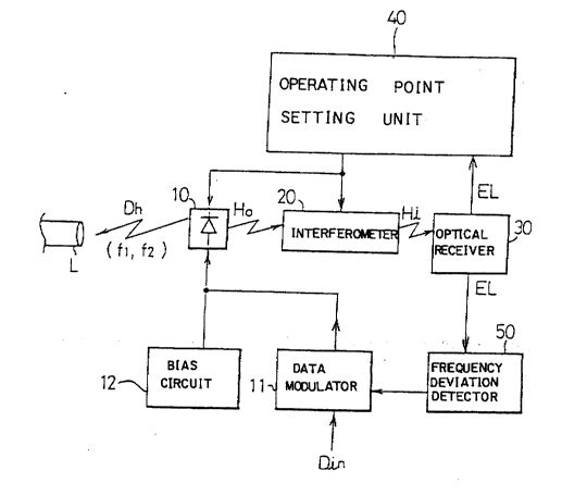
In Fig. 1, the f~rward light of a semiconductor
laser 10 is ~ransmitted to a t~nsmission li.ne L as
light data Ph. A control signal may be extracted from
the ~orward li~ht~ The }iqht da~a Dh is sub~ected to
opti~al frequen~y modula~ion ~f1, f2) or phase
modul~tion in a~cordanoe with logic levels 1 and 0 of
data Din ~o be transmit~ed. Tl1e modula~ion wi~h data
Dln i~ performed by a data modul~tor 11. A well-known
~ias circuit 12 is provided for performing the
modulation under the optimu~ drive conditions.
C05t~ tuent elements 20, 30, 40 and 50 other than
the elemen~ 10, 11 and 12 COnstitUte the measu~e and
control device of the pre~ent invention. The measure
and control device operates in response to reception
of output liqht ~Io of the s~miconductor laser 10, for
example, its backward ligh~. As shown, the measure
and control device is comprlsed of an interferometer
20, an optical ~ecelver 30, an operatlng point settinq
means 40 and a fr~quency deviation detector 50.
PQ2n
2060943
The interferometer 20 receives the output light
Ho of the semiconduCtox laser 10 an~ outputs
interference liyht Hl in accordance with its optical
fre~uency discriminating ~haracterlstics.
S Th~ optical receiver 30 receives the int~rference
light Hi and converts its intensity to an electric
~i~nal EL~
The operatin~ point settlng means ~0 receives the
electrlc s~.gnal EI. and ~ets the oper~tlng point of the
interferometer 20 ln such a way that the operatin~
point always corre~ponds with the maximum value o~ ~he
minimum value of the optical frequen~y di~crimin~ting
characteri stic5 .
The deviation detector 50 receives the electric
1 S slgnal EL outp~t from the optieal receiver 30 under
the stabilized operating point and detects the ave~age
value of t~le li~ht intensity. A difference between
the average value and a set value corresponding to the
fixed optical frequency deviation ls fed back to the
data modula~or 11.
The principle of the operation of the optical
frequency devlation and control dev.i.ce fo~ a las~r
light ac~ordlng to the fir~t aspect o the present
invention is based on the two following polnts:
: ~5 ~1) stabili~ing the operating point of the
~02
- 206~94~
18
interferometer to correspond wi.th the maximum optical
frequency o~ the m~nimum optical ~r~quency o~ the
optlcal frequency discrlminatinq characteristics of
the inter~erometer; and
(2) under the ~t~illzed ~ t~llg p~int,
detecting ~he average ~alue of the li~ht intensity of
~he interferenee light ~li and feedlng the averà~e
value back to the data modulator 11 so as to allow the
average value to converge to a ~et value t~f the light
lntensity ~hen a predetermined optical fre~uency
deviatlon is produ~ed.
The operatlons of (l) ~nd ~2) ~re mainly
performed ~y the operating settlng means 40 and the
deviation detector 50, respectively,
Fig. 2 is a graph o the optical frequency
discriminating characteristic of the interferometer.
In the gr~ph, the abscissa indicates the optical
frequency~ i.e., the o~er~ting frequency of ~he
interferometer 20 and the ordinate indlcates the
intensity P of the inter~erence light Hi from the
lnterferometer 20. As the in~er~erometer ~0, any of
Fabry-Perot lnterferome~er, Michelson interferometer
and Mach-Zehnder inter~erometer, etc., are applicable
whi~h ~r~ ~ll w~ll kllowrl. T~l~ yraph indi~ates ~he
frequency discriminating eharacter~ ~tlc ob~erved by
2060943
the Mach-Zehnder interferome~er.
In general, the opti~al frequency discriminatiny
charaeteristic di~lays a sin~soidal va~iation of the
light intensity with ~he variation of the optical
S frequency. The graph in Fig. 2 indicates part of the
cha~ac~eristic. ~s shown, the light intensity assumes
the maximum value MAx and the mlnlmum v~lue MIN. The
optieal frequencies w~ich allow the light intensity to
assume the n~aximum v~lu~ MAX and the minimum value MIN
are fmax and fmin, respeeti~ely. In the present
invention, the operating point (the centr~l optical
frequency fO b~twecn the fir~t and second optlc~l
frequencie~ fl and f~) is set so as to always maintain
either of the maximum and minimum valu~s of the li~ht
intensity. That is, the ope~atlng frequency of the
int~rferomete~ 20 ls set ~o fma~ or ~min.
Now, let u~ ~onsider the optical frequency
dRvlaLi~n ~E of the fir~t ~nd 3ccond optioal
~requencies f1 and f2 from the centr~l optical
frequency fO with the operating $requency as fmax.
When 4f, like ~f'in ~ig, Z, i5 smaller than the
prede~ermined de~iation ~f, the llght int~nsity P' of
the interference ligl-t ~1i resulting from ~f' ls
greater than the predetermined light inten~ity P
resulting from ~f. Conversely, when ~f, llke ~f''
Po23
2060943
~o .
in Flg. 2, Is l~rger than ~f, the llght lntena~ty P"
resulting from .~f" i~ ~msller ~han the predetermlned
li~ht inten~ity P fron~ Af .
In thi~ ca~e, both en~ of ~f ~ ~f ~ and ~f ~ ~
corr~pond to the flr~t and ~econ~ ~eq~enci~ nd
f2. Actually~ each of the tran~ition~ f~om f1 to f2
and f2 to f1 takes place alon~ the curve of the graph
of Pig. 2. Thu~ it heco~es posslble to monitor the
optical frequency devlation in term~ o~ the average
value Pav of the light lntenslty P.
~ lg. 3 i~ a gr~ph lllu~tratln~ averag~ value of
light inten~ity versus optical ~req~ency devlatlon.
In the grapll, a solid line indicates the relationship
when the operating point is set a~ the ~aximum valu~
MAX a~ ln t~lQ above ex~mple, whllo the chain .~.lne
lndicates the relationsh~p when the operatlng polnt is
set as the ~inimum value MIN. In the case where the
operating point ~s set a~ the maximum value MAX as in
the above example in Fig. 2, while the optical
frequency devia~lon .~ become~ ~maller ( ~f') or
larg~r I ~f'')~ the Average value Pav of the llght
intensity becomes larger ~Pav " ~ or smaller ~P~v'~.
Fig. 4 ~hows experimental data for substantiatlng
that the graph of Fig. 3 can be obta~ned. In the
graph, the abscl9sa indicates the outp~t voltage of a
P024
2060943
21
pattern pulse ~enerator which corresponds to the
modulation current to a laser dlode for ~imulating the
optical fre~uency devia~lon, whilo the ordinate
i.ndlcates th~ ~urrent flowing th~ough a PI~ diode fo~
5 simulating the average value of the liqht lntensity.
In this graph, the curve plotted by white dots
corresponds to the characteristic indicated by the
solid line in Flg. 3, while the cur~e indicated by
black dots corresponds to the characte~istic indicated
by the br~ken llne in Fiy. 3.
In the device o Fig~ 1, the opexatin~ point
setting means 40 is provided by taking account of the
gr~ph of Fig~ 2, while the deviation detector 50 is
provided by taking account of the graph of ~ig. 3.
The feature of the present inVentiOn is to use the
light i.ntensi~y of the lnterference l~g~t Hi as a
control variable arl~ treat only low-f~equency
componen~s of ~he lLght intensity. Thus, the measure
and control devlce according to the first aspect of
the present inventlon may be a device WhiCIl iS ~lmple
in const~uctlon and operates at a very low ~requency.
FLg. S is a basic: bloek diagram ~f an optical
frequency deviation measure arld control device for ~
laser li~ht a~cording to a second aspect of the
25 present inventlon.
Po25
- 2060~43
In the f lgure, a semicon~uctor laser 110 output~
output light ll10 having its optical frequency shi~ted
to a fir~t optlcal frequency fl and a s~cond optical
frequency f2 ln accordance with logic levels 1 and 0
of a high-rate modulating signal. That is, the outpu~
light of th~ semiconduct~r la~r is sub~ected to
frequency-shlft keying.
The optical frequency deviation mea~ur~ and
control ~evice for a laser light accordlng to the
second aspect of the present inventlon operates in
response to reception of FSK mod~lated output l~ght
H10 from thc semiconductor laser 11 n a~ S shown,
comprlses an interferometer 1~0, an optical ~eceiver
130, an operatlng point setting means 140 and an
optical frequency deviation detector 150.
The interferometer 120 is responsive to the
outpu~ light H10 o~ the semiconductor laser 110 to
output interer~nce light H1i depending on it3 optical
frequenoy discrlmina~iny characteri~tics.
The optlcal receiver 130 receives ~he
interference llght H1i and converts its light
intensity to an electric slgn~l EL10.
The operating point setting means 140 receives
the elect~ic signal ~L10 and sets the operating point
25 of the interfRrometer 1 20 ~o that it corresponds to
P026
2060943
the opt:lc2.l frequency corre~3ponding to the value which
is mtdway between the maximum value and the ~inlmum
value of the optical f~equency discriminating
characteristic.
The op~lcal freguency deviation ~e~ector 150
extracts a low frequency signal component of the
average light output intensity of the interference
light H1 i which has been modulate~d wlth ~ low
frequency in ad~ance under ~he operatin~ point from
O the electric signal ~L10 by means of sync~ronous
detection and detect~ an optlcal f~equency deviatlon.
The principle of the operation of the optical
f~equency deviation measure and ~ontrol devlce fcr a
laser light according to the second a~pect of the
pr~sent invention ;~ based on the two followin~
points:
~1) sta~ilizing the operating point of the
intcrferometer 1~0 at the optical ~requency
corresponding to the value which is the median value
O between th~ maxlmum value and the m1nimum value of lts
optical frequencv discriminatlng characteristic; and
(2) und~r the stabiliz~d opcrating point,
ext~acting a low-frequency signal component of tlle
aver~ge llght output intensity of the interfer~nce
light 1~1i which is outpu~ modulated with a low
Po~
- 2060943
24
frequency in advance from the interferometer by mean~
of ~ynchronous detection of the ele~tric signal EL10
from th~ op~ical receiver 130 with a low frequency
si~nA1 ~nd de~ectinq an optical ~req~ency deviation
from the synchronous-detected output ~ignal.
The operation~ tl) and (2) are mainly performed
by the operating point setting means 1~ and the
optical frequency devlation detector 150,
respectively, as will be described below in more
detail.
1 0
~ ir~t, of the op~ratinq p~int will be described~
Fiq. 6A ls a graph illust~ating the optical
frequency d~scrlminating characte~istiC of th~
interferometer 1 20 . In the graph, the abscissa
indicates the operating requency of the
1 5
interferometex and the ordinate indicates the light
intensity P of the interference light H1i rom the
interferometer 120. ~rhe interfer~nce l$ght H1 i
contains two components H1ia and H1ib which are
complement~ry to e~ch other. In Fig. 6A, the ~olid
curve indlcate~ the optical frequency d~scriminatin~
characteristic of the interfexence light component
H1 ia and chain line indlc~es the sa~e charact~ri~tlc
of ~he interference light eomponent H1ib. As th~
interfero~eter 1Z0 in the device according to the
Po28
2060943
second asp~ct, any of the ~abry-~erot int~rferome~er,
the Mlchelson. interferometer, the Mach-Zehnder
interferometer, etc. are appl~cable, which a~e a~l
well known. The graph of ~ig. 6A indlcate~ the
S optical ~requen~y ~iscriminati~g char~t~ristic o~ the
Mach-Zehnder inter~erometer.
As ~hown, the li~ht intcnsity assumeS the maximum
value MAX and the minimum value MIN. The optical
frequency producing the maximum value ~AX is fmax,
whlle the optical frequency producing the minimum
value MIN is fmin. In the pxesent invention, the
operating point (the central optic~l f~equency fO
~etween t.he ~ st And ~econd optlcal frequ~3ncies f1
and f2) is set to correspo~d to the medlan v~lue ~E~
15 (frequency ~med) of the maximum and minimum values at
all time~,
The addition o~ the two in~er~erence light
compo"ents H1la and Hlib, which are complementary to
each other, will produce a flat output as indicated by
20 a chai~ lin~ in Fl~. 6A. The flat outpu~ ~ ~
proportional to the light output of the semicond~ctor
laser 11 O . On the other other hand, the subtraction
of the two complementary components H1 ia and H1 ib will
double the amplltude as shown in Fig. ~ and the
~esultant output erosse~ the z~ro point at the median
P029
I
2060943
26
value ME~, i.e., the operating point . Thus , by
controllin~ the bias or temperature of the
semi conductor 1 aser 1 10 or ~he interferomet~r -I 20 so
that the Bignal resulting from the subtraction of the
complementary interference li~ht components ~1 ia and
H1 lb becom~s zero at all times, the ope~atin~ point is
allowed to st:ay at the median value MED o~ the optical
frequency discriminating character~sti~,
Next, the detec~ion o~ tho optical freques)oy
1~ deviation wlll be descri.bed.
It is supposed here for the purpose of
si~plifying description that the output light H10 of
~he semiconductor laser 110 ha~ been subjected to
ideal FS~ modulatlon of a ~a~k rate of 1/2. The mark
15 rate refers to the ratio between 1s and Os in a
nodulating ~ignal. If ~ 1 and a O eacl1 occur at equal
probability, then the mark rate w~ll bc t /~. If the
ratio hetween 1s and Os is 1 to 3, then the mark rate
will be 1/4. The ideal FSK modul~tlon means that the
20 tran~i~ion 'cime betw~n the first optic~l ~requoncy f1
and the seccrld o~tic~l freq~ncy ~2 le infinit~mal.
The operating point i~ stabilized at the median
value ~ED of the optical fre.~uency discriminating
characterlst~c as ~lescr ~ bed above, This state is
shown in Fig. 7A. For convenience, the optical
Po30
2060943
frequency deviation 4f i~ set such as ~f = FS~/2.
Ilere, FSR refers to the optical frequency differenc~
between ad~ acent ~aximum ( minimum ) values of the
optical frequency discriminating characteristic in a
5 free ~pect~al range. Th~ ht output is varied with
a low-~requency signal with the operating poin~
stabilized a~ the median value MED. If, as ~hown in
Fig. 7B, the operating point shifts to the right, e~ch
of the optical fre~uen~ies f1 and f2 will also shift
to the ri~ht. Consequently, the light output ~1 at
tlle opti~al freque~cy ~1 increases, while the optical
output P2 at the optical frequency f2 decreases. If,
as shown in Fig . 7C, the operating point ~hifts to the
left, each of the optical frequencies fl and f~ will
also shift to the left~ Consequently, the light
output P1 at the optical frequency f1 increases, while
the optical output P2 at the optic~l frequency f2
d~creases. The variations in the ~ptical outputs P1
and P2 are observed as va~iations in the average light
output ~ntensity from the i.nter~erometer 120. ~ere, a
variat~on o~eu~s in the phase and amplitude of the
varying average light output intens~ty from the
interferometer 120, depending on the magnitude o the
optic~l frequellcy deviation ~E (= fl- f2), whlch will
~5 be descri~ed below.
Po3
2060943
28
8A shows the case w) e~e ~f i~ small.er than
FSR/2. In the figure, when the operating point i~
shifted to the riqht by a low-f~quency signal S1, the
optical frequencies f1 and ~ shift to the right, so
5 that the li~ht outp~ts at f 1 and f 2 increase . When
the oper-Ating polnt ~ 5 shifted l:c~ Lll~: l~$t~ 1 he
optical ~requencies f1 and f2 shi~t to the left, so
that the l igl~t outputs decrease. Thus, the ~verage
light output intensity will vary a~ shown at the r1 ght
of th~ figu~e.
~ i~. 8B shows the oase where ~f - FSR/2. In
this ~ase, since f1 and f2 shi$t on a complementary
basis as also ~hown in Fig. 7B, the increment and
decremen~ of the light output are equal to each other.
Thus, although the operating point is changed wlth a
low-frequency ~ignal S1, there i5 no variation in the
average light output intensity as shown at the right
of Fig. 8B.
Fig. 8c show~ the case where Qf ) FSR/2. In the
figure, when the operating point i~ shifted to the
ri~ht by a low-~requen~y ~ignal S1, the optical
frequencies fl and f2 shift to the right, so that the
~ i.ght outputs at ~1 and ~2 decreaSe. When the
operating point is shifted to the left, on the other
hand, the optlcal frequencie~ f1 and f2 ~hift to the
3 P032
- 2060943
~9
lef'c, so thAt 'che li~ht ou'cputs at fl and ~2 inc:rea~e.
Thus, the avera~e ligh'c outpu~ intensl~y will var y as
shown a~c the right of the figure. The variation in
the average light output intensity ln Fig. 8C in which
5 ~f > FSR/2 is o~posite in phase to th~t in ~ig. 8~ in
which ~f ~ FSR/2.
As described above, the amplitude and phase of
the variation in the average light outpu'c intensity
vary accordiny to the magni tude o~ t~l~ optical
~ ~equency deviation af . There~o~e, the conve~sion of
the ave~age light output intenslty f~om the
int:erferome'cer 1~0 to an ~lectric signal ln the
optical receiver 130 and the synchronous detection o
the elec~ric signal ~ith the lo~-f~guency signal S1
15 permi~ t~e magnitude of 'che optical $requency
deviation ~f to be obtained.
Fig . 9 shows optical f requency deviation .~f
versus synchronous detection output signal of the
average li~ht output intensity. Either the signal
lndica~ed by a ~olld line or the output slgnal
in~icated by a chain line is output dependlng on the
phase of ~ ~e~erence signal for synchronous detection
indicating whi~h of posltive and negativc slope~ of
the optical ~requency di~criminating characteristic
~urve th~ operating point i~ set on. Here, the
-- 2060943 P~33
deviation of ~he synchronous detection output signal
from zero represents the deviatlon of the optical
frequency deviation ~ f~om ~R/2. ~hen bf = FSR/2,
the synchronous detection signal is zero~ There~y, if
t.he synchron~us ~etecti~n olJtput gignal is m~asured,
the value of the optical ~requency devlatlon 4f will
be measured. Thus, it will be seen th~t lt is
possible to measure and control the optical frequency
deviation.
In the d~vice of Fig. 5, the operating point
setting means 140 i~ provided taking a~count of the
~raph o~ ~ig. ~ and the optical frequency deviation
detector 150 ~ provlded taking ~ccount o~ the graph
of Fig. 9. The feature of the present inven~ion is ~o
use the ligh~ lntensity of the inter~erence light H1i
as a control variable and handle only a low-$requency
component of the li~ht intensity. The~efore, the
rneasure arld control device according t.o the ~econd
aspect of the pre.~ent lnvention m~y be A 8~vlce which
is simple in con~truction and ope~ates at a ve~y low
frequency.
Fig. 10 is a ba~ic block diagra~ of an optical
frequency deviation measure and cont~ol device for a
laser ligh~ acco~dlng to a third aspect of the presen~
invention~
P03~
. I
2060943
31
In th~ fl~ure, a s~miconduct:or l~cr 210 outputs
output ligh~ ~120 having its op~ical frequency shifted
to a first optical frequency f1 and a second optical
frequency f2 according ~o lo~ic levels 1 and O of a
5 hi~h-spe~d modulating signal~
The measure and eontrol device ~ccording to the
thi.rd aspec~ of the present invention operates in
response to the FSK modulated output light H20 from
the seln~conductor laser 210 an(3, as shown, ~omprises
10 an lnterfero~eter ~20, an optlcal recelver 230, an
operatin~ point se~tin~ means 2~0 and an optical
~equency deviation detector 250.
The interferometer 220 is responsive to th~
output light 1120 of the ~emlconductor lase~ 210 to
15 OU~:pllt interEerence light H;~i depending on its optic:al
freq~lency disc~iminating characteristics.
The optical receiver 230 receives the
in~erference light H2i and converts its li ght
lnten~ity to an electric slgnal EL20.
The operating point setting means 240 detects the
oper~tinq point of the interEerometer ~20 by
extrac~ ~ ng f rom the electric siçlna~ EL20 a low-
frequency si~nal of the interference si~nal H2i which
has been low-frequency modulated by means of
synchronous de~ection and sets the operating point of
Po35
- 2060~43
the interferometer 220 so that it corre~ponds to the
optical frequency corresponding to the maximum value
or minimum value of the optical frequency
discrim1 natin~ chat-Acteri~tic.
The optical frequency deviation detector 250
extracts a low frequency signal component produced
under the operating point from the ele~tric signal
E~,20 by means of synchronous detQction and detects ~n
optioal frequency deviation.
The Principle of the operation of the an optical
frequency deviation measure and control devlce f~r` a
laser light according to the third aspeot of the
present invention is based on t~e two following
poin t s:
(1) stabilizing the operating point of the
interferometer 220 at the optical ~requenoy
correspondlng to ~he maximum or mlnimum value of the
optical frequency discriminating cha~acterl~tic of the
in~erferometer 220; and
~ (2) under the ~tabilized ope~sting point,
extracting a low-frequency signal component S22 which
is twi.ce a low-frequency signal S21 of the avera~e
light output in~ensity of the in~erfe~ence li~ht 1~2i
which is output, modulat~d with a low f~equency in
advance, from the interferometer 220 by means of
P036
I
33 2060943
synchronous detection o~ the electric signal EL20 from
the optical receiver 230 and detecting an optical
freq~ency deviation from the synchronous-detected
output signal.
The operations (1) and (2) are mainly per~ormed
by th~ operating ~o; nt setting means 240 and the
optlcal frequency de~iation detector 250,
res~ectively~ as will be describéd below in more
detail.
First, the setting of the operatiny point will be
descr ibed.
Fig. 11A is a graph illustrating the optical
frequency di~crilllirlA~iny cha~acterist~c o~ the
int~rerometer 220. In the graph, the abscissa
15 ~ ndicates the optical frequency input to the
interfe~ometer 220 and ~he ordinate indic~tes the
light in~ensity P of the interference light H~i from
the interferome~er 220. The interfcrence light H2i
contains two complementary components H2ia and HZib.
ln F~g, 11~, ~he ~olid line indicateS ~he optical
frequency discriminating charactC~istiC of the
interference light component HZia and the chain line
~ ndicates the like characteristic of the interference
light component HZlb. As the interferometer 2~0, any
of the Fabry-Perot inter~erometer, the Michelson
3 P031
_
34 2060943
inter~erometer, the r~ltAch-zehr~ lnterferometer, etc~
are applicable, which are all well known. The g~aph
of E; ig . 1 1 A indicates th~ optical fxequency
discriminating ~haracteri.stic of the ~a~h-Zehnder
5 inter~erometer.
As shown, the light intensity assumes the maximuln
value MAX and the minimum value MIN. The optical
frequency produclng the maximum value MAX ls ~max,
while the optic~al fre~uency producing the minimum
10 value MIN is fmin. In the present lnvention, the
o~erating poin~ (the optical fr~quency fO which is
~edian value between the first and second optical
frequencies fl and f2) is set to corre~pond to either
the maxlmu~ value or the m~nimum value.
The add~tion of 'che two interierence light
components H2ia and H2ib, which are complementary to
each other, will produce a flat output as indlcated ~y
a chain line in ~ig . 1 1 A. The flat output is
proportional to the light outpu'c of the 9emicondu~tor
20 lase~ Z10. On the other hand, the subtraction of the
two complementary inte~eren~:e components ~12ia and
H2ib will double the amplitude of the output as shown
by a solid line ln Fig. 11 B. A signal resulting from
synchronous de~ection of the subtracti~n signal with
~5 the low-frequenc~y signal S21, whic~h has been
P03~
2060943
superimposed on ~he bias of the semiconductor laser
210 or the interferometer 220, i~ equivalent to a
w~fo~m which is oht~ine~ hy dif~erentiatinq the
subtraction signal, or a waveform lndicated by a
chain line in Fig. 11~. Thus, the synchronous
detection si~nal becomes zero a~ the maximum value MAX
and the minimum value ~IN. Therefore, by controlling
the synchronous detection signal to follow the zero
point at all times, the operatin~ point can be set to
corr~spond to th~ maximum v~ e MAX o~ the minimum
value MIN of ~he optlcal requQncy dl~cxlmin~ting
characte~istic.
The de~ection o~ the optlcal fre~uency deviation
will be descri~ed next.
Fig. 1 2 A, B, C illu~trate spectra of light
ouLputs of the interfe~omete~ ~0 when an FS~
modulated light signal is received and the ope~ating
point is swept. In this case, the Mach-Zehnder
interferometer is u~ed. As ~he optlcal frequency
a~
=~ . 20 deviation ~f ~mod~lation index) becomes greater, the
spectrum of modulated light signal beco~es wider.
.~, ...
Thu~, the cohe~ence of llgh~ becomes worse, and th~
Ypectrum of light ou~put from the interferometer 2~
broadens as shown in Fig. 1 Z. In Fig. 1 2, the
2S ma~nitude of the optical frequency deviation ~ ~
P039
I
3~ - 2060943
becomes greater in the order A, B, and C and the
speetral waveforms of the average l~ght outputs become
gentler accordingly.
The synchronous detection of the light outpu~ by
5 the low-frequency s~gn~l S21 permits the operating
point to be stabilized at the m~ximum value MAX or the
minimum value MIN of the spectrum at all times. When
the operating point is stabilized at the maximum value
M~X, the ~vcr~g~ 1 iqht outp~t ~rom th~ 1 nterferometer
10 220 ls observed a~ a deforme~ waveform of the low-
frequency signal S21 a~ shown in the center of Fig.
1ZA, B~ C. When the operatin~ ~oint is present at the
maxlmum val~le MAX, the the low-~re~u~n::y signal
component S21 ~ecomes minimum, Instead~ the low-
15 frequency signal component S22, whose frequency is
twlce that of the low-f~equency co~ponent S21, is
produced most ~trongly. The amplitude of the low-
~requency si~n~l compon~nt S22 represents the ~radiell~
of the shoulder of the spectrum. Since the gradient
20 varies with the magnitude of ~, f as shown in Fi~. 1 2A,
B, ~, the amplitude of the low-frequeney signal S22
corresponds to ~ f.
Fig. 13 shows a ~elationship between a.signal
~ft.er ~ynchronou~ ~tectio~1 by ~he low-frequency
25 signa~ S~2 which ls twice the low-frequency signal S21
~. P040
37 2060943
in frequency and the optical ~requency deviation ~f.
A value of ,~f is measur~d on the l~asis of the graph.
~hat is, by de~ectin~ the low-frequency ~ignal
component S22 indicating variations in the aver~e
5 light output intensity of the interference light H2i,
whi~h is produced under t~ ilized operat1ng
point, with l ~le low-frequency slgnal S~2 and making a
onmpAriSon between the detected sign~l and a set value
of ~he synchronous detection output signal which
10 produces a p~edeter~ined optical frequency devi~tion
~f, ~f can be detected. The feedb~ck to ~he data
modulator so that the set ~alue of the dete~tion
siqnal will be reached wi.ll make stabilization of the
op~ical ~requency dev~a~ion (modul~tion index)
15 possible~
In the device of Fi.~. 10, the ope~ating point
setting means 240 is provided taklng note of t~e graph
o~ Fig. 1 1 and the optical frequenCy deviation
detector 250 i~ provided taking nOte of the graph of
~o Fi~. 13. The feature of the pre~ent lnven~ior, is to
use the light intensity of the interference light H21
a~ a control variable and handle only a lo~-frequency
component o the light intensity. There~ore, the
device for measurlng and controllin~ the optlcal
~s frequency deviation o~ the semiconductor laser
P~4
2060943
accordin~ to the third aspect of the present invent~on
may be a devlce which is si~ple in construction and
operates at ~ very lvw fre~uency.
In the above de~cribed ~irs~ to third aspec~s,
S the sta~ at~on o~ an oporat~n~ ~int o ~a~e~ light
is controlled by synchronous de~ection, etc, throu~h a
synchronou~ detecting circuit. On the other hand, ~n
the fourth and fifth aspect~, controll~n~ operation
such as synchronous detec~ion, etc. is not requlred
for the stabilization control of an operating polnt.
Fig~re 14 is a basi.s block diaqram of a fourth
aspect o~ the present invention.
In Fl~ure 14, laser light H30 is a backward light
outpu~ted by a semi.conductor laser 319. Forward li~ht
1S outputted by the ~emiconductor la~er 319 is applied to
the transmi~sion line ~not shown ln Flgure 14) as
optlcal data. Then, the optical frequency of thc
laser light H30, is subjected to frequency or phase
modulation into either a Eirst or a ~econd optical
~requency with the predetermined central optical
frequency ~operatin~ point) based on the drive current
provided ~y a data modulator 320 according to the two
l~gic values 0 an~ 1
A light interferenc~ unit 304 responsive to the
laser light H30 emits inter~erence llght depending to
. ~ P04~
-
2060943
the optical frequency di~criminating character~stlc~.
The light interference unit 304 comprises a first
polarizer 303 1nserted therein.
Then, a flrst ~4 plate 30~ and a second
5 polarizer 307 for accep~ing light ~IB1 reflected from
thc light interference ~nit 304 through a half mi~ror
321 are sequentially positioned.
A flr~t optlcal receiver 312 and a second optical
receiver 313 receive two types o~ light HB3 and HB3
10 resp~ctively and convert the light int~nsity of each
typ~ of light to an electr1cal signal EL31 and EL32
~espectively.
Th~n, a feedback unit 314 fee~s back the
o~clllating frequency of the laser llght H30 or the
1S interference charac~eristic~ of th~ light interference
unit 304 according to ~he information lndicating the
phase difference be~ween two o~thogonal directlonal
components of the laser llght H30 obtained from the
d~ffer~nce co~pone.n~.s between the electri~al signals
EL31 and EL32 ~rom the first and ~e~ond op~ical
receivers 31~ and 313 so that the operating point o~
the laser light ~I30 correspond~ to the optical
frequency corresponding ~o the maximum or mini~um
value of t:he optical frequency dist~riminating
characteristic~. Namely, the feedback unit 314 feeds
-- 2060943
28151-51
back, accordlng to the slgnal obtalned by subtracting the
electrlcal slgnal EL32 from the electrlcal slgnal EL31, the blas
or the temperature of the semiconductor laser 319 or of the
light interference unlt 304 that outputs the laser light H30.
On the other hand, a thlrd optlcal receiver 317
recelves transmitted llght H31 from the llght lnterference unlt
304 and converts lts light lntenslty to an electrical slgnal
EL34.
Under the stabillzation control on the operating point
of the laser llght H30 by the feedback unlt 314, an optical
frequency deviation stabillzer 318 calculates the dlfference
between the average value of the llght lntenslty of the
transmltted llght H31 obtalned by the electrlcal signal EL34
from the third optlcal receiver 317 and the predetermlned value,
and then feeds back the dlfference to the modulation factor of
the laser light H30. For example, the dlfference ls fed back to
a data modulator 320 for performing modulatlon according to
lnput data Dln.
Flgure 15 ls a basls block dlagram of a flfth aspect
of the present lnventlon.
The flfth aspect shown ln Flgure 15 is dlfferent from
the fourth aspect shown ln Figure 14 in that not a polarlzer but
a second ~/4 plate 401 is lnserted lnto a llght interference
unlt 402 and a third polarlzer 403 ls lnserted between the llght
interference unlt 402 and the thlrd optlcal receiver 317.
The fourth and flfth aspects respectlvely shown ln
Flgures 14 and 15 can be, llke other aspects of the present
lnventlon, appllcable to the FDM transmlsslon system. In thls
~.,
~ .~.
" ~.
2060943
41 28151-51
case, each of llght lnterference unlts 304 and 402, polarlzers
303, 307, and 403, and ~/4 plates 306, and 401 operates wlth a
plurallty of the laser llghts H30 each havlng a dlfferent
operatlng point. The corresponding number of optical recelvers
312, 313, and 317 to the number of laser llghts H30 are
parallelly positioned for receiving HB3, HB3', and H31 (H32)
respectively. The feedback unit 314 and the optical frequency
deviation stabilizer 318 shown in Figures 14 and 15 respectively
perform parallel or time divisional operation for each laser
light H30. Specifically ln thls case, the feedback unit 314
causes an operatlng polnt of each laser llght H30 to correspond
to any of a plurality of optlcal frequencles correspondlng to a
plurallty of maxlmum or mlnlmum values of one optlcal frequency
dlscrlmlnatlng characterlstlc of the llght lnterference unlt
304. Then, the frequency of each laser llght H30 can be
automatlcally controlled by feeding back a signal to control the
blas or temperature ln each laser
~ ~,
~,
Pnn
42 2060943
31g outputting e~ch laser light H30.
In the fourth and ~ifth a~pects respectlvely
shown in Figures 14 and 1 S, an automatic llght output
controller can be provided for feeding back the
5 o~cillation output of the laser light ~30 according to
~he electrical si~nal EL33 from a part of the laser
light 1130 or the third optical receiver 317 so that
the oscillation ou~put of thé laser li~h~ H30 ean be
stabili~ed to a predetermined value.
The operational principle of the fourth and fifth
aspects of the measure and control device for a laser
light as configured above is gener~lly identical with
the fir~t aspect of the present invention and
summarized as follows:
15 1 ) An operating point of laser llght mu~t be
stabilized to the optical frequency corresponding to
the maximum or minimum value of the optic~l frequency
discrl~inating characteristics in the llght
interference unit.
2) Under the stabilized operating polnt, an average
value of the in~erfe~ence light intensity must be
detected and measured, and the modulation factor of
the laser light must be fed back so that the average
value can ~e converged towards the set va~ue for the
li~ht intensity when a predeter~ined deviatlon of
,, P002
.. . I
2060943
optical frequency is produ~ed.
That is, the present inventiOn adopt~ the
prineiple that an average value of l$ght intensity and
th~ optical frequency deviation have ~ specific
5 functlon relatlon to ea~h other when an op~rating
polnt of l~or light ( ~nt~al optical frequenc~)
corr~ponds to the optical frequency correspondin~ ~o
the maximum or Minimum value of the optieal requency
diseriminating char~eristics of the light
10 interference unit.
As degcribed above, in the fourth and ~ifth
aspects respectively shown in Figures 14 and 15,
stabllization control on an operating point of laser
light can be perormed, as a pre-proce~s or
15 stabilizing the optical ~requency deviation of laser
light, without additional controlling operation such
as synchronous detection, eto. as descxibed in the
firs~ to third aspects of the present lnvention.
That is, as shown in Figu~es 14 and 15, ~he first
20 ~ 4 plate 306 and the second polarizer 307 are used
with each of m~in axis slanted at predetermined
degrees. ~hen, the information indicating the phase
difference between two orthogonal polarization
~:umE~ ents of the l~scr l~ght HB1 ~an be oht..q 1 ned in a
25 form~t comprising an item "sin ~ indicates phase
PoO3
_ .. i
44 2060943
difference) as a difference signal between the
electrical si~nal EL31 o~ the ~irst optical receiver
312 and the electrical signal EL32 of the ~e~ond
opti~l L-eceiVer 31 3. U~ing such inf~rmation of a
5 phase difference, the maximum or minimum point in the
optical frequency discriminating characterietics may
correspond to the zero point ~indlcating that the
a~plitude ls zero) of the above desc~ibed difference
slgnal.
Based on the fact above, an operating point ~an
be contro~led such that an operating point in the
las~r light li30 constantly co~responds to the optlcal
f requenc~ corresponding to the maximum and minimum
value of the optlcal frequency discriminating
15 characterlstics of the li ht interf~rence unit 304
~ s;g~l ~ ~o nt~r
using the ~eedback unit 314 for feeding back the bias
or the temperature of the laser 309 or the light
lnterferen~e unit 304 according to the above de~cribed
diff~rence s igna 1, etc . .
~0 The difference between the ~ourth and fifth
Aspects respectlvely shown in Fig~res 14 and 15
resldes ln that the lock-in-ranqe of an operating
point of the laser light EE30 can ~e lBrger in ~he
fifth aspect than in the fourth aspect.
The fourth and fifth aspects of the presen~
2060943
inventlon descrlbed above can be appllcable to the optlcal
communlcatlon systems ln the optlcal frequency-dlvlslon multl-
plex (FDM) transmlsslon method. Speclflcally ln thls case, as
the feedback control operatlon ln the operatlng polnt stabll-
lzatlon control ls performed on the osclllatlon frequency of
laser llght, each operatlng polnt of each laser llght (central
optlcal frequency) ls set on a plurallty of maxlmum or mlnlmum
values respectlvely ln one of the optlcal frequency discrlml-
natlng characterlstlcs of a llght lnterference unlt. Thus,
automatlc frequency control (AFC) of each laser llght can be
performed slmultaneously. The lnterval of the optlcal fre-
quency between the ad~acent maxlmum and mlnlmum values of one
of the optlcal frequency dlscrlmlnatlng characterlstlcs ls a
flxed value. Therefore, as a result of the slmultaneous
executlon of above descrlbed automatlc frequency control,
operatlng polnts of respectlve laser llght ln the FDM trans-
mlsslon system can be arranged at equal lntervals on the
optlcal frequency axls.
Explanatlon of the Preferred Embodlments
Flg. 16 ls a block dlagram of a flrst embodlment of
the present lnventlon. Herelnafter, llke parts are shown by
correspondlng reference characters throughout all the vlews of
the drawlngs. The present embodlment
X 28151-51
POQ5
2060943
4~
shows a speciic ~orm of each of the opexating setting
points 40 (Fig. 1 ) and the deviation det~cting means
50 (~i~. 1). First, the operatlng setting means 40
compri~es an operating point detector 41 and an
S o~era~ing poin~ controller 42.
In order to va~y an osclllation frequency a~ the
operating point ln the optical frequency
discriminating characteristic, the oper~ting point
detector 41 controls the oscillatton fr~quency of the
10 semiconduct~r laser 1 0 or the lnterference
characterl~tic of the interferometer 20 by way of a
control line L1. ~he operating point controller 42
receives an electric signal EL which varie~ fxom the
; optical receiver 30 with varyln~ operating point and
15 shifts the operating frequency according to the resul~
of the reception ~o that the operating frequency
converge~ ta th~ ~aximum ~luc MAX o~ the minimum
value MIN. To shift the operating point, the
oscillatlon ~requency of the semiconduc~or laser 10 or
20 the interference characteristic of the interferometer
21 is controlled throu~}1 a con~rol line L~.
The devia~ion detecting m~ans S0 comprises a
coln~)~rator 51. The c.omp~rat~r receive~ e direct
current component of the electric signal at its first
input ter~inal and a predetermined set voltage V1 ~t
P006
.~ 2060943
q7
its second input terminal. The output of the
comparator is ~ed to the dat~ modulato~ 11 . The set
voltage V1 corresponds to V1 in ~he graph of Fig. 3~
The optical frequency deviation a f corresPonding to
S Vl i~3 to ~c held constant.
Fig. 17 illustrates a specific arrangement of
each o~ the operating point detector and the operatin~
polnt controller of Fig. 1~. The operating point
detector 41 (Flg. 1 6 ) consis~s me~ely o~ a low-
frequency oscillator 43 which varles the oscillatlon$requency of the semiconductor laser 10 or tlle
interference characteristic of ~he interferomet~r 20
at a low frequency. The low ~requency means that it
is low in comparison with the frequenCy of a data
transmlssion speed, and it is, for example, 100 llz.
On the oth~r hand, the ~ erating point controller
42 ~Fig. 1~) consists m~rely of a synchronous detector
44. The synchronous detector is responsive to the
electric si~nal EL from the optical recei~er 44 and
the oscillator output of the low-~requency oscillator
43 to perForm synchronous detection on the electric
sign~l and ~xtrAct ~ signal com~onent synehronized
with the o~cillator output. Further, the synchronous
detector controls the bias of the semiconductor ~aser
10 or the interferometer 20 via the control line L2
,~"3 PG07
2060943
48
using the extracted slgnal component applied thereto.
It i 8 ea 5 y to vary the inter~erence
characteri~;tic of 'che lnterferometer at a low
requency and the bias of the interferometer.
5 Basically~ th~ length of t~le resonator of the
interferome~er and the delay time difference have only
to be varled. Specifically, there ~re known the
following methods of utilizing:
(1) the phntoelastic effect;
~) the electro-optical effect;
(3) mechanical external force; and
(4) the thermal optical effect,
The oscillation ~re~uency ~f the semiconductor
lase~ 10 can be varled by controlling its drive
current, The bias of the semiconductor laser c~n be
v~ried by ~ontrollir~ the ~ias circuit 12.
Here an additional explana~ion ~111 be made o~
the op~ration of the low-fre~uency oscilla~or 43 and
the synchronou~ detector 4 4 ~
Flg. 18 is a waveform diagr~ for use in
explanation of the operation of the low-frequency
oscillator. The figure particularly shows an exalnple
where the output of the low-freq~ency oscillator is
superimposed on the drive current of the semiconductor
~5 laser. The ~rive cur~ent is indicated by Ip.
Pnl2
2060943
4g
~ar~ing the d~ive current Ip to have two valu~s, the
frequency of the output lig~1t Ho of the semiconductor
laser 10 ls shlft~d to th~ first optical frequ~ncy f1
and the second optical frequency f2 with the frequency
~0 cente~ed. When, in this state, tl1e output of the
low-f~equency oscilla~o~ 43 i~ 6uperimposed, the dri~e
current winds with the oscillato~ fr~quen~y fl like a
wave as shown. The electric signal ~L containing the
low-frequency component is subjected to synchronous
detection in the syncl1ronous detec~or 44 responsive to
the output of the osc~llator 43.
Fic~. 1gA is a wav~r~ dlagram o~ a synch~onous
detection signal ~hen the Mach-Zehnder int~rferometer
is used, while Fig. 17B is a like waveform diagram
when the Fabry-P~rot inter~erometer is used. For the
purpose of better understanding, the corresponding
optical frequency discriminating characteristic is
shown at the ~op of each of th~ synchronous detection
signal waveform diagrams. These optical frequency
discriminating eharacteristics correspond to the
graph of Fig. 2.
The si~nal resulting from the syncl1~onous
det~ction is equiva~ent to a waveform obtained by
differ~ntiating the optical freq~ency discriminating
cha~acterist,~,c as descr~.bed in connection with Fig.
Po13
2 0 6 0 9 4 3
11 B. Thu~ , the synchronous detection ~ignal become~
zero at the maximum value MAX and ~he minimum value
MIN ln the optical frequency discrimina~ ng
char~cte~i~tic, For this rea~on, lf the zero p~int c~
5 the synchronous detectlon signal i~ always followed,
the operatinq point will continue to be ~et at the
maximum value MAX or l:he minimum value ~IN.
The above description was made in connection with
control fc~r keeping the optical frequency deviation
10 constant. The automa~ic frequency con'crol (APC) may
be performed at the same time. This is re~lized by
feedlng the ou~pu~ of the 8ynchronvu~ detector 44 back
only tc~ the ~em~.çnn~n~t.c~r laser 10 in ~lg~ 17, so that
the center optical frequency fO is maintalned at a
15 de~ired cc~nst~nt value.
Furthermore, the automatie light output control
(APC) can be per~ormed at ~he same tlme. To reallze
the APC, however, there ls a need ~or an
interferometer whlch splits the output light HO of the
2~ ~cmiconductor laser 1~) lnto two complemQntary
interference light components (H~ Hib~. In this
case, two optlcal receivers (31, 32) are needed to
receive the two complementary inter~erence light
components, Th~ two optical receivers will be
25 described later.
2060943 P014
Fig. 20A i1lustrates ~.he Mac~l-Zehnder
interferometer ~hich outputs t~o complementary
interfe~ence light components and Fig. ~OB illustrates
the optical frequency discriminating characterist.ics
of the two intererence light compon~nt~. In ~ig.
20a~, M de~ignates half mlrrors and M' de~ignates
mirrors. A p.redetermined difference in length i5
p~u~uce~ be~ween two light pH~hS to ther~by p~ducQ
two complementary lnte~ference light co~ponents Hia
and Hib~ The two complemen~ary interfe~e.nce light
components Hia and Hib have such optical frequency
discriminating characteristics as shown in Fig. 20B.
~ he same analysis can be applied to the Fabry-
Perot inter~erometer.
Fig. 21 ~ illustrates Lh e Fab~- P erot
interferometer which outputs two complemen~ary
in~erference light components and Fig. 21B illustrates
the optical frequency discriminating eharacteristies
o the two in~erference light component5~ In fig.
21~, the interferenoe li~ht Hia is transmitted light,
while thc ;nter~eren~ light Hib is re~lected light.
I~ is .~o as not to return the re~lected light Hib to
the ~emiconductor laser 1~ that the Fabxy-Perot
interferometer FP is s].anted wlth respect to the
optical axis of the output light ll~. Note that there
Po15
2060943
52
are othe~ means for obtaining two complementary
interference light components.
~ ig. 22 illus~rates another means for obtaining
two complement~ry interference light componen~s.
According to this means, a ~irst polarizer PL1 and a
second polarizer Pl.0 are p~ovided at tle input and
output sides of a double-ref~action crystal CR,
resp~ctively~ and two complement~ry inte~f~rence light
~ omponents Hi~ and Hlb are obtained from the output
10 l ight ~lo .
HereinA~ter, a clescriptivll will be m~e of ~n
optical requency deviation me~sure and control
device for a laser light ~sLng the two ~omplementary
; interfer~nce light components ~a and Hib which are
obtained in the manner des~ribed above.
F~g, 23 is a block diagram of measure and
control device according to a second embodiment of the
present invention, which incorporates intcrfer~meter
21 (refer to Figs. 20A, 21A and 22) whi~h outputs two
complementary interference light components Hia and
Hib and two optical ~eceivers 31 and 3~ for receivlng
the two interference light components. Electric
signals ~Ll and EL2 output from the optical rec~ivers
31 and 32 arc add~d to~eth~r in an ~dder 47 to produce
their sum signal. The sum ~ignal is fed b~ck to the
2060943 P016 I
s3
semiconductor laser 10, so that the light output o~
the semiconductor laser 10 can be kept constant at ~ll
times. In practice, volta~e ~ignals corresponding to
the electric signal~ EL1 and ELZ are added together.
For the addition of voltages, voltaqe detecting
resistors 45' and 46' and an instrument ampliiers 45
and 46 are provided .
The reason why the APC can be perfor~ed by the
output of the adder 47 will ~e mad~ clear by referrlng
10 to Fig. 20B. The additiol1 o~ the two interf~r~nce
light components Hia and Hib, ~hich are complementary
to each together, will produce a flat output as
indica~ed by a chain line in Fig. 20B. ~hat ls, the
a~ditlon vf ~hc electric si~n~l~ EL1 ~n~ E~2 in the
adder 47 produces a flat outp~t signal. If the
feedback is made to the semiconductor laser 1~ so that
the level of the flat output signàl will remain
constant ~ all times, the APC will be realized. In
~i~. 23, an ~PC control cixcuit 48 detects a ~eviation
in the output of th~ adder 47 from a pre~et value V2
for feedback to the semiconductor laser 10.
In this case, as the illpUt to the synchronous
detector 4 ~, the output of t~le me~surement ampl if ier
45 or 46 is used.
In the a~rangement of Fig. 23, a difference
2060943 POi7
54
signal of the electric signals E~1 and EL2 is used as
the input to the optioal frequency deviation detecting
means 50, The difference signal of the electrl.c
signals EL1 ~nd EL2 is equivalent. to ad~ition of the
broken cu~ve to the solld cur~e with the forme~
reversed in polarity in ~ig. 3. Thus, suoh a ~ignal
havin~ a greater rate of variation aS shown by a dash-
dotted line in Fig. 3 is obtained. In other words, .it
becomes posslble to control the Optical frequenoy
deviation ~itl1 ~ signal havin~ a ~teep ~La~ien~ This
incre~ses the S/N ratio in the control of the optlcal
requency deviation.
In Fi~, 3, lf adiustment is made so tha~ the
; optlcal frequency deviation at the int~rsection X of
the solid ~urve (~orresponding to Hia) and the broken
curve ~corresponding to Hib) becomes a desi~ed optical
frequency de~iatiorl, it will ~e ~b~ained when the
difference signal of the electric signals EL1 and ~L2
become zero. That is, the deviation detecting means
~0 50 has only to provide fc~dback to the data modulator
11 so that the difference signal o~ EL1 and EL2 al~ays
converges towards ze~o.
It ls easy to adjus~ the lase~ light properly so
that the desired optioal f~equency deviation can be
25 obtained, ~he ad~ustment is realized easily ~y
P018
206094S
changing the free ~pectral rang~ (FSR), ch~nging the
finess of the interferometer 21 and ch~nging the
relative amplification factor ~f the optical rec~ivers
31 and 32, the optical coupling rate, the quantum
5 efficiency, etc. The ~rranqement of Fig. 23 can be
modi~l~d as ~llown in Flg. ~. rn thls c~e, the above
ad~ustment can also be made by changing ~he relative
amplification factor of the measurement ampli~iers 45
and 46.
~ig . 24 illustrates a modif ication of means for
taking the dif ference signal in the embodiment of Fig .
23. In this modiflcation, the difference signal of
~L1 and ~LZ is ob~ained fLom a su~l ract~r 5Z.
~igure 25 is a block diagram of a third
embodiment of the present invention.
~ he e~bodiment is applicable to a~ optical
frequency-division multiplex (FDM) transmlssion
system, that is, an optical communica~ion system for
processing cen~ral optic~l frequency simultaneously in
;~ a single optical Liber t~ multipleY. and transmit
lnformation of a plurality of lines.
~ semiconductor laser 15, a data modulator 16, a
bias uni~ 17, an interferometer 2~, and an optical
receiver 33 shown in fig. 2~ correspond to 10, 11, 12,
25 2û, and 30 of the first embodiment shown in Figures 16
P019
- 206094
s~
and 17. An operating point ~tabilizer 49 shown ln
Pigure 25 co~respond~s to the low frequency oscillator
43 and ~ynchronous detecting circult 44 shown in
Fi~ure 17, whiJe an optic~l f~equency deviation
5 stabilizer 54 ~hown in Figure 25 corresponds to the
comparator 51 shown in Figure 1~.
The third embodiment shown ln Figure 25 ls
different from the fir~t embodiment shown in Figures
16 and 17 in the ~oin~ that the ~ .ransmis~l~n
system requires a plurality of central optical
~requ~ncy, while e~ch of the semiconductor laser 15,
d~ta mofl~ t.~ 1 6, bias unit 17, optical r~ceiver 33,
operating point sta~ilizer 49, ~nd the optlcal
frequency deviation stabiliz~r 54 comprises a
plurallty ~ n of units, thereby realizing
multiplexed transmis~lon of trans~is~ion data ~in of a
plurality ~1 - #n of lines. The light interfe~ence
means 22 compr~ses, in thls embod~ment, a Fabry-Perot
interfer~meter. Each of ~ n backward light l~o
provided by each of #1 - ~n semlconductor laser is
sp~tially divided by n optical ~iber and led ~y ~ne
unit of Fa~ry-Per~ inte~erometer 22, while ~cl- of
interference ligh~ Hi is spatially divided by n
optical ~lber and led by n opti~al receivers 33.
~5 The stabilizi~g operation of an operating polnt
2060943
,
57
and optical frequency deviation by ~ semiconductor
l~Ber 15 ~n each o n part in #1 - #n s~ts ~own ln
Flgure 25 a~e basicelly the same ~s the flrst
e~bodiment shown in ~lgure9 16 and 17.
HOWQVer, in this embo~i~ent~ th~ Ouep~t ~
each of th~ oper~tlng polnt stabilizer 49 (corresponds
to the low frequency oscillator 4~ and synchronous
dotectin~ circuit 44 of the first embodlment shown ~n
~iguro 17) i8 8up~rimposed and negatively fed back to
the bias cùrrent ln each bias unit 11 or to the
control in~l~t. of the te~peratu~Q control eloment of
each semiconductor laser 15. Thus, each operating
point of each laser light tcent~al op~ l r~-equency)
of each semiconductor laser 15 is ~et to n p~nts
15 ind~cating the maximum value MAX (Figure 191~) of t~ e
optical ~requency discriminatin~ characteristics of
lnterferometer 22. Then, the interval of the optlcal
frequen~y between ad~acent maximum value points in one
optical frequency discriminating characteristics is
~0 ~Ssigned a fixed value. Therefore, as a result of
slmultaneous realization of each autom~tic frequency
COntrol ~ ~FC) on e~ch laser l~ght of o~h
semiconductor laser 15 as described above , n operating
points of #l - ~n .semiconduct-~r laser t 5 in the FbM
transmission system can be positioned exactly at equal
2060943
intervals in an optical frequency axis.
Th~ optlcal frequenoy deviation celn be stabil.ized
to each predeterrnined value i~or each laser ligh~ of
each semiconductor laser 15 unde~ ~he above described
5 automatic ~requency control ~ AFC ) .
Further, a plurality of l~ r light ~pplled to a
single peak value of either ~h~ m~ximum or minimum
value of the optical ~requency diseriminating
characteristics enables tra~smission at a common
frequency through different t~ansmlssion lines.
Figure 26 is a block dia~ram of a ~ourth
em~odiment of the presen~ in~ention. In Flgure 26,
all parts assigned the same numbers a~ ~hose assi~ned
to the third embodiment have the ~ame functions
5 respectively.
The fourth embodlment is different fr~m the third
embodiment in ~he poin~ that an operating point
stabilizer and an optical fre~uency deviation
stah:i1i.zer are 61 and ~2, each ~mprising a ~in~le
~0 unit, and each unit is operated in a time divisional
manner.
The output pro-~ided by each of #1 - ~n optical
~,~3 rec:eivers ~3 is applied to the operating point
~tabilixer ~ and optical frequenCy deviation
,.,~.., ...., ~. ~
25 st~bilizer ~ through switches 63 ~nd 64. Each ~c
59 2060943
control resul~ is stored in data storages 67 and 68
hrou~h swit~hes ~5 and 66. I~ch ~ the ~d s~o~geY
67 and 6~ ~egatively feed back the latest ~ontrol data
ff1 ~ #n ~t ea~h co~rol point simultaneou~ly to each
S bi~s unit 17 (or a temperature control terminal of
each ~emiconductor laser 15) and each data ~odulator
16, thus reducing the circuit scale in the above
descrihed configuration.
In thlLs embodiment, the modulation o~tput for
1~ synchronous de~ection provided by the oper~ting point
stabilizer ~ (corresponding to the oscillation output
of the low ~requency oscill~tor 43 in the first
em~odimen~ shown in Figure 17) is superlmposed to the
interf~rometer 22, thereby elimlnatin~ the necessi ty
of low fr~.qt2ency modulation of optical frequency of
- each laser light from each s~miconductor laser 1S.
Therefore, the influence of low frequenCy modulation
component on the modulatiorl co~ponent corresponding to
an essential communication signal of each laser light
csn be comple~ely eliminated.
Fig. 27 is a block dlagram of a fifth embodiment
o~ the present invention.
I~ the fi~re, ~orward ligh~ of semi~ond~ctor
laser 110 is ~ransmitted to a transmission line (not
shown)a~ optical data Dh. A control signal may be
2060943
-
~aken from the forward light. The optical data Dh has
been su~ected to optical frequency modulation or
phase modulation accord$ng to logic levels 1 and O of
data Din to ~e trans~nitted~ The modulation with the
S dal:~ ~in to be transmitted i~ per~or:rned by a
modulation circuit 111. Though not shown, a well
~nown bi~s ~ircuit is connected to the semiconductor
laser 110 in or~er to perform the optieal modulation
~nder the optimum drive conditions.
10The device o~ the present invention operates in
~ponsc to rec~pti~n of FSK mod~latcd ~tput ligh~
~t10 ~rom the semiconductor laser 110, which consists
of backward light. Interferometer 120 receives the
: outpu~ light ~10 from the semiconductor laser to
15 produce two complementary interference light
comporlentS ~1 ia and H1 i};) accordin~ to their optical
~requency discriminatin~ ~har~ct.~istics.
Examples of an interferometer adapted to produce
two complementary interference light components are
illustrated in Figs. 20A, 21A ~nd 22. The op~ical
frequency di~criminating characteristics of ~he two
eomplementary in~erference light components H1ia and
H1ib are illustrated i~ ~ig. 6A.
Referring back to ~ig. 27, two optical receiver~
~5 131 and 136 are provided for receiving the two
F;
61 2060943
interference light components ~tia and II1ib. Each o~
the optic~l receivers may compri,se a photodiode. The
interference light components H1 ia and H1 ib are
respectively converted to -elec~ric signals EL11 and
S EL1~ which indicate their light intensity. In a
subtracter 141 and an adder 143, voltage signals
Correspon~lng to t}l~ el~tri~ signal~ EL11 ~nd EL12
are sub~ec~ed to subtrac~ion and addition. To this
end, there a~e provided voltage detectlng resistors
132 and 137 and ins~rument amplifie~s 133 and 138.
The subtracter 141 outputs the difference between
the electric si~nals ~L11 and ~12 f~om the opti~al
rece i ver s 13 1 and 13 6 .
The adder 143 outputs the sum of the electric
signals EL11 and EL1~.
In the present em~odiment, the oper~tin~ point
setting mean~ 140 comprises an operating point control
circuit 142 and an ~PC control circuit 144.
The operatlng point ~021trol ~ircuit 142 uses the
20 dif ference signal of the electric signal~ E3.11 and
EL12 fr~m the subtrac~er 141 as an operating point
detecting signal and makes ~he operating point
corre~pond to the median M~ between the M~X and the
MIN of the optic~l frequency discriminating
characteristic at all times. The methods of shifting
- 2060943
62 28151-51
the operatlng point includes a method of providing feedback to
control the bias or temperature of the semiconductor laser 110
via a control line Lll to control the oscillation frequency of
the semiconductor laser 10 and a method of provldlng feedback to
control the bias or temperature of the lnterferometer 120 vla
the control line Lll to control the lnterference characteristic
of the interferometer 120. Both of the methods may be used ln
comblnation. In the case of feedback to control temperature, a
known Peltier devlce is used. Slnce the two interference light
components Hlia and Hlib are complementary to each other, the
dlfference therebetween crosses the zero polnt at the medlan MED
as shown in Flg. 6B. Namely, the use of the dlfference slgnal
of the electrlc slgnals ELll and EL12, whlch crosses the zero
polnt at the medlan MED, as the operatlng polnt detectlng slgnal
and the provlslon of feedback to control the blas or temperature
of the semlconductor laser to the bias or temperature of the
lnterferometer permlts the operatlng polnt to be stablllzed at
the optical frequency at whlch the dlfference slgnal becomes
zero. In the case of feedback to control the bias or
temperature of the semiconductor laser, the control of the
operatlng polnt frequency also permlts the osclllatlon frequency
~o60~43
63
of the outp~t light Hl O of the ~emiconductor laser to
be controlled. ~hus, the stzlbilization of the
operating point and ~utomatic frequency con~rol (~pc)
of the semicond~lctor laser c:an be performed at ~he
S same t itne .
The APC control circult 144 uses the sum of the
e~ectric signals EL11 and EL12 ~rom the adder 143 aæ
an optical ou~put detec:ting signz~l and comprises a
~omparato~ whi<:~h ~eceives at its firs~ input the
10 optical o~ltp~.lt detectil~y ~Lgnal ~nd ~t its s~ n~
inpu~ a predetermined ~et voltage V1 l . The control
circuit detects a difference ~etween the set voltage
V1 1 and the optical output detecting signal and
provides feedback to the bias of the semiconductor
5 laser 1 10 via the control line L1~ so that the
difference ~ay become zero at ~ll times. Since the
two interference li~ht components ~1ia anA H1ib are
relative to ea~h other, the addition thereof will
pxoduce a flat output as indica~ed by a dash-dotted
2~ line in Fig. 6A. The ~lat o~tput is proportional to
the light output of the semiconductor 1~ser 110.
Namely, the automatic light output control (~PC) is
re~li.zed by set~inq the voltage V11 to cor~espond to a
fla~ signal obtained by addition of the electrL~
25 signals E~1 1 and ~Ll 2 and prov~ding feedb~ck to the
_ 64 2 0 6 0 9 4 S 28151-51
semiconductor laser 110 so that the level of the flat slgnal may
become constant.
The optical frequency deviation detecting means 150
comprises a low-frequency oscillator 151, a synchronous detector
152, an optical frequency deviation stabilizing circuit 153 and
an amplifler 154.
The low-frequency oscillator 151 varies the
osclllatlon frequency of the semlconductor laser 110 or the
interference characteristic of the interferometer 120 through a
control line L13 at a low frequency in order to vary the
oscillation frequency at the operating point in the optical
frequency dlscriminating characteristic. The low-frequency is
used hereln to mean that it is low in comparison with the
frequency of a data transmission rate and is, for example, 100
Hz. The operating point is varied by a low-frequency signal
whose speed is higher than the response speed of the operating
point setting means 140. The low-frequency signal Sl is used as
a synchronous detection signal in the synchronous detector 152.
By superimposing the low-frequency signal Sl on the bias or
temperature control slgnal of the semlconductor laser or on the
bias or temperature control signal of the lnterferometer 120,
the osclllatlon frequency at the operatlng polnt is varied.
Although the operation of the low-frequency oscillator
151, like the operatlon of the low-frequency oscillator 43
illustrated ln Flg. 17, can be explalned by referrlng to the
waveform dlagram of Flg. 18, lt ls omltted hereln. The electrlc
slgnals ELll and EL12 containing a low-frequency component are
detected by the synchronous detector 152 uslng the low-frequency
~,~,......
2 060 943 28151-51
osclllator output.
It is easy to vary the blas of the lnterferometer 120
as in the case of the lnterferometer 20 descrlbed prevlously.
The explanatlon thereof is omltted hereln.
Referrlng back to Flg. 27, the synchronous detector
152 detects the dlfference slgnal component of the electrlc
slgnals ELll and EL12 from the subtracter 141 uslng the low-
frequency slgnal Sl whlch ls the synchronous detectlon slgnal
from the low-frequency osclllator 151 and extracts a slgnal
component synchronlzed wlth the synchronous detectlon slgnal.
The signal component extracted by the synchronous detectlon ls
the optlcal frequency devlatlon detectlng slgnal whlch ls used
to measure an optlcal frequency devlatlon. Herelnafter, the
measurement of the optlcal frequency devlatlon ~ f ln
?1,~
2060943
6~
the synch~onous deteotor 152 will be descri~ed.
When the operating point of the ~SK modulated
optical signal i~ st~ilized at the median MED ~etween
the MAX an~ the MIN o~ th~ optical fxequQn~y
discriminating characteristic of the interferometer
120 and the op~ratin~ ~; nt is shifted b~ the low-
frequency signal 51 o the synchron~us deteGtion
sign~l, the phase and amplitude o~ variations of the
average light output intensity vary ~ccordin~ to the
10 m~gnit:ude of the optical frequency deviation ~ ~ as
shown in Fig~ 8. Thus, the magnitude of optical
frequ~ncy de~riation ~ ~ can J3e obtained by c~nverting
the average l lght output intens i ty f ~om th~
intererometer 120 to an electric signal and detecting
15 the electric signal usin~ the ].ow-frequencY signal S1~
A relationship between the optical frequency
deviatlon ~ f and t~e synchronous detection output
sign~l for the avera~e light outp~t intensity is
illust~ated in Fig. g. In the figure, a deviation ~f
~he ~ynchronous detection output signal ~rom zero
represents a deviation of the optical frequency
deviation ~, f from FSR/2. When ~ f = FSR~2, the
synchronous detec~ion output signal be~omes zero.
~hat ls, the measurement of the synchronous detection
output si~nal is equivalent to the measurement of ~.f.
~7
2060943
The optical freq~ency de~iation stabilizing
circuit 15~ may comp~ise a ~omparator ~hich receive~
its first input a deviation detect signal o~talned
by the ~yn~h~onous detector 152 and at its s~cond
S input a preset volta~e V1~ ~nd provides f~edback to
the modulation circuit l 11 so that the difference
therebetween ~a~ become zero. Thereby, t~e opti~al
frequen~y deviatlon ~f tmodula~ion index3 is kep~
con~tant.
1 A8 an input to th~ synchronou~ detector 152 use
is made of th~ dif~erenoe signai of th~ electrie
si~nals EL11 and E~12. The difference signal is
equivalent to addition of a broken curve to a ~olid
curve in Fig.~ wlth the ~o~mer reversed in polarlty.
In other words, the optical requency deviation ca~ be
controlled using a signal having a steep gradierlt.
This permits ~ considerable increase of the stN ratio
in th~ optical ~re~uenoy devi~tion control.
The amplifier 154 is provided, in superimposing
the synchronous detection signal from the low
frequency osclllator 1 S1 on the )~ias of the
semiconductor las~r 110 via the control line L13, for
~eeding the optical frequency deviation dete~t signal
fr~m the optical frequency deviatiOn fitabilizlng
circuit 1S3 back to the modulation amplitude of the
2060943
low frequency signal S1 which is the synçhronous
detection modulation signal so that the optical
~requency deviation of optical f~equency modulation by
the modulation signal may be made constant and the
5 optical frequency deviation de~ecting means 1 S0 may
not be affected by the modulation e~ficiency of ~he
light source of the ~emic:onductor laser 110.
~ hat is, when ~he FM modula~ion ef f iciency
~ optical frequency v~riation per unit bias current )
10 becomes ~mall beca~se of ~gin~ ~hange of the bias o~
L~e s~mi~onduc~or la~er itsclf, tho low frequency
signal S1 may not be superimposed in the worst case.
Thus, the operat~ing E~oint may not vary as set and l~ho
synchronous detection may ~ecome impossible. 'rO avoid
15 this, the amplifie~ 1~4 is used to make large the
amplitude of the modulation signal ~or synchron~us
deteGtion when the FM efficiency becomes small and to
make small the amplitude o~ the modulation si~nal when
thc FM effi~iency become~ ~oo lar~e. Th~t. i ~, the
20 low-frequency signal 51 is controlled to have
sub~tantially the ~a~e amplitude. ~he ma~nitude of
the FM rnod~lation ef ficiency is determined on the
basis oi the magnitude o~ the optical frequency
deviation a f .
~S A mark rate ~onitor mcans l~O may comprise an
~ 2060943
lntegrator in the modulation circuit 111. Th~ unitol-
mea~s ~ontrols the operating state of the optic~l
frequençy deviation detecting means 150 by calculatin~
the probability that logic level~ 1 and 0 will occur
in data modulation in which the fre~uency of the
output light H10 of the semiconductor laser 110 is
~hiftcd to the f;.rst and secon~ ~requencie~ f1 and f2
in accordance with logiG levels 1 and 0 of data to ~e
transmitted.
Fig. 7A i~ a graph when the mark rate is 1/Z.
When the mark rate is 1/4, that is, 1s and Os o~ur in
the ratio of 1 to 3, the avera~e l~ght output
intensity moves to the top right in Fig. 7~. For this
; rea~on, the gr~ph of Fig. 9 varies with the result
tha~ the value of ~ f when the synchronous detection
o~tput signal becomes zero will vary ac~ording to the
magnitude of the mark ~ate. ThUs~ it is required to
change the set volta~e V12 of the optical frequency
deviation stabilizlng circuit 153 according to the
~ ma~k rate. The m~rk rate monitor 160 c~lculates the
mark rate of modulation signal of the modulation
circult 111 and change the set voltage Vl2 according
to the calculated mark rate, ~o thereby ~ontrol the
operating state of the optical frequency deviation
~5 detectlng means 150. That is, a mark rate m~ni~or
70 2060943
6iqnal o an input mod~tion si~nal is fed back to
the optical frequency devlation ~tabilizin~ circuit
153 with ~he result that the circuit is not aff~cted
by variation ln mark rate.
Fi~. 28 is a block dia~ram of a sixth embodlment
o the pre~ent invent~on.
In the figure, forward li~ht of a semiconductor
laser 2~0 ~s transmit~ed to a transmission llne not
shown a6 optical dat~ ~h. A cont.rnl ~ignal may be
ta~en rom the forwa~d light, The optical data Dh has
been subjected to optical frequency modulation or
phase modulation according to logic levels 1 and 0 of
data Din to be transmitted. The modul~tion with the
data ~in to be transmitted ls performed by a
15 modulation c~ircl~i.t 21~. Though no'c shown, a well
known bias clrcuit is connected to the semico~ductor
laser 210 in order to perform the opti~al modulatlon
under the optimu~ drive condit.ions.
The device o~ the present inventlOn operate.~ in
~ response to reception of ~SK modulated ou~put light
~I~0 from the ~emiconductor lase~ 210, which con~ t6
of ba~kwar~ ht. A~ interferometer ~0 receives the
output light H20 from the semiconductor laser to
produce two complementa~y interference light
co~ponents H2ia and H2ib a~cording to their optic~l
2060943
71
frequency disc~iminating char~cterlstics.
Examples of an interferometer adapted to produce
two complementary interferen~e light components are
lllustrated in Figs. 20~, ~lA an~ 22. The aE~t.ica~
fxequency discriminating characte~istlcs of the two
complementary interference light components H~ia and
H2ib a~e illustrated in Fig. 11A.
Referring back to Fig. 28, two optical receivers
231 and 232 are pro~ided for recci~ing the two
- 10 interference lig~t components H2ia an~ ~2i~,
respect~vely. Each of the optical receivexs may
comprise a photodiode. The interference light
components H2ia and H2ib are re~pe~tively converted to
electric si~nals ~L21 and EL22 which indicate their
light in~ensity. In a subtracter ~37 and an adder
238, voltage signals eorresponding ~o the electric
signal~ EL21 and EL22 are subjeet~d to subtraction and
addition. To this end, there are provided voltage
detecting re~istors 233 ~nd 234 and lnstrument
amplifiers ~35 and 236.
The subtracter 237 outputs the ~l~fe~ence between
the electric signals EL21 and ~L22 f~om the optical
receiv~ro 231 a~d 232.
The adder 238 ou~puts the sum of ~he electric
signals EL21 and EL22.
2~60943
72 28151-51
In the present embodlment, the operatlng polnt settlng
means 240 comprises a low-frequency osclllator 241, a
synchronous detection circuit 242, an operating point
stabilizing clrcult 243, two adders 244 and 245 and an ampllfier
or attenuator 246.
The low-frequency oscillator 241 produces a low-
frequency signal S21 and varies the frequency at the operating
polnt in the optical frequency dlscrlmlnatlng characterlstic at
a low frequency. The methods of shlftlng the operatlng polnt
lncludes a method of providlng superlmposltlon on the blas or
temperature control slgnal of the semlconductor laser 210 via a
control llne L21 to control the osclllatlon frequency of the
semiconductor laser 210 and a method of provldlng
superimposition on the bias or temperature control slgnal of the
interferometer 220 via the control line L21 to control the
lnterference characteristic of the lnterferometer 220. Both of
the methods may be used in combination. In the case of feedback
to control temperature, a known Peltler devlce ls used. The low
frequency ls used herein to mean that lt is low in comparison
wlth the frequency of data transmlsslon rate, and for example,
100 Hz.
The synchronous detector 242 recelves the dlfference
slgnal component of the electrlc signals EL21 and EL22 from the
subtracter 237, which is used as an operating point detecting
signal, and the low-frequency slgnal S21 from the low-frequency
osclllator 241 and extracts a slgnal component synchronized with
the low-frequency signal S21. The slgnal after the synchronous
detection is equivalent to a waveform obtained by
,.. .
-_ 2060943
73 28151-51
differentlatlng the optlcal frequency dlscrlmlnatlng
characterlstlc as descrlbed ln connectlon wlth Flg. llB. Thus,
the synchronous detectlon slgnal becomes zero at the maxlmum
value MAX and the mlnlmum value MIN in the optlcal frequency
dlscrlmlnatlng characterlstlc. Thus, the operatlng polnt can be
made to correspond to the maxlmum value MAX or the mlnlmum value
MIN by causlng the operatlng polnt stablllzlng clrcult 243 to
converge toward zero. That ls, lf feedback ls provlded to the
blas or temperature control slgnal of the semlconductor laser
210 or the blas or temperature control slgnal of the
lnterferometer 220 so that the synchronous detectlon slgnal may
always become zero, the operatlng polnt wlll be stablllzed at
the optlcal frequency at whlch the synchronous detectlon slgnal
becomes zero. In the case of feedback to the blas or
temperature control slgnal of the semlconductor laser 210, the
control of the operatlng polnt frequency also permlts the
osclllation frequency of the semlconductor laser
2060943
to be controlled. Thus, the stabilization of the
op~.rating poi~l~ and a~omatic frcq~ncy con~rol ~FC)
of the semiconductor laser 210 ca~ ~ performed at the
same time.
The APC control circuit ~7 uses the sum of the
electric si~n~ls ~;L21 and EL22 from the adder Z38 as
an optical output detecting signal and m~y comprise a
eo~parator which receives at its first input the
~E~tical output det~3c~iny s~gnell ~nd at its ~econd
input a predetermined set voltage V21 . The APC
c:ontrol circuit 247 detects a c3ifference be~ween the
set voltage V21 and the opti~al output deteeting
signal and provides ~eedback to the bias of the
semi~onductor laser 210 vi~ the control line L22 so
~hat ~ e different.e may become zero ~t all tlmes.
Since the two interfexence light components E~2i~ and
I~2ib are c:omplementary to each other, the addition
thereof will produce a flat output as indicated by a
chain line in Fig . 1 1 A. The flat output is
proportional to th~ light outpu~ of the semiconductor
laser 210 ~ Nan~ely, the automatic light output control
~APC) is realized by setting the volt~yte V21 to
correspond tc) the flat signal obtatned by addition of
the electric signals EL21 and EL22 and provldin~
feedback to the semi~onductor laser z10 so that the
2060943
28151-51
level of the flat slgnal may become constant.
The superimposltion on and the feedback to the
temperature control signal of the semlconductor laser 210 from
the low-frequency osclllator 241 and the operating stablllzlng
clrcuit 243 and the superlmposltlon on and feedback to the blas
or temperature control slgnal of the lnterferometer 220 are
comblned ln an adder 244. Also, the superlmposltlon on and
feedback to the blas control slgnal of the semlconductor laser
210 from the low-frequency osclllator 241 and the operatlng
polnt stablllzlng clrcult 243 are comblned ln an adder 245.
Although the operation of the low-frequency osclllator
241 llke the operatlon of the low-frequency osclllator 43
illustrated ln Flg. 17, can be explalned by referrlng to the
waveform dlagram of Flg. 18, it ls omltted hereln. The electric
signals EL21 and EL22 contalnlng a low-frequency component are
detected by the synchronous detector 242 using the low-frequency
osclllator output.
It is easy to vary the blas of the lnterferometer 220
as ln the case of the lnterferometer 20 descrlbed prevlously.
The explanatlon thereof ls omltted hereln.
The optlcal frequency devlatlon detectlng means 250
comprlses a second low-frequency osclllator 251, a second
synchronous detectlon clrcult 252 and an optical frequency
deviatlon stablllzing clrcuit 253. The second low-frequency
oscillator ls a multlpller whlch recelves a low-frequency slgnal
S21 from the flrst low-frequency osclllator 241 and produces a
low-frequency slgnal S22 whose frequency ls twlce that of the
slgnal S21.
,iiB
.. . .
76 2050943 28151-51
The second synchronous detectlon clrcult 252 recelves
the dlfference slgnal of the electric signals EL21 and EL22 from
the subtracter 237 as an optlcal frequency devlatlon detectlng
slgnal under the condltlon that the operatlng polnt of the
lnterferometer 220 ls stablllzed at the maxlmum value MAX or the
mlnlmum value MIN of the optlcal frequency dlscrlminating
characterlstlc by the operatlng point settlng means 240. It
also recelves the low-frequency slgnal S22 from the second low-
frequency oscillator 251 as a reference signal for synchronous
detectlon and performs synchronous detectlon on the dlfference
slgnal to extract the low frequency slgnal S22, thereby
detectlng an optlcal frequency devlatlon.
Having descrlbed ln connectlon wlth Fig. 12, when the
low-frequency slgnal S21 from the low-frequency osclllator 241
ls superimposed on the bias or temperature control slgnal of the
semlconductor laser 210 or the
k
F~ 0
2060943
inter~ero~nete~ 220 to shift the ~p~r~iny point, the
low frequency signal componen~ S22 whose frequency ls
twice that of the low frequency signal S21 appe~rs
most strongly in variations in ~he average light
S intensity of the interferometer 220, The ampl$tude of
~he signal S~2 co~responds to ~he magnitude o~ ~ f.
This is ~ased on the fact that the detect signal ~fter
the synchronous dete~::tion of an electriC s~ ~nal
correspondln~ to the light inten~ity with the low
f~equency signal S22 and the optical frequency
deviation a f have such ~ relationship as show in Fig,
1 3 .
If the low fxec~uency signal S~Z, whos~ frequency
is twice that of the low frequency signal S21, of the
15 average light output intensity of the int~rference
llght H2i which has be~n modulated wi~h the low
frequency æignal S21 previously is extracted by
synchronous detection using the low frequency slgnal
S22, then an optical fre~ency deviation det~cting
20 sign~l will be obtained. In this case, ~s the optical
frequency devi~tion detecting signal to thc second
synchronous detection circuit 252 the dif ference
component of the electric si~nals El21 and EL22 from
the subtracter 237 is used. The diffe~ence signal is
doubled in amplitude as shown in Fig. 11B, The
-
78 2060943
optic~l frequen~y deviation ~f can be detected usin~ a
si~nal h~ving a steep gradient. Thi~ wi}l increase
the S/N ratio in the optiçal frequenCy deviation
control.
The optical f.reqllency de~riation stabilizing
~lxcuit 253 m~y comprise a comparator which receives
at its first input a deviation detecting ~ignal
o~tained by the second s~chronou5 detector 25~ and at
its second input a preset voltage V22 and provides
feedbeck to the modulation circuit 211 so that ~h~
dif ference theteb~tween may converges toward zero~
The set volta~e v22 ~or~esponds to volta~e V~2
corresponding to a prPset optical f requency deviation
~ f in the g~aph of Fi~. 13. The set volt~e V22
corresp~nds to the optical frequency deviation a f to
h~ k~pt constant. The control of stabilization of the
optical frequency de~iation ~modulation index) will
a 1 s o bec ome pos sible.
The ~mplifier ox attenuator 246 is provided, in
~0 superimposing the low frequency signal S21 which is a
modulation signal for synchronous detectlon sign~l
~rom the low frequency oscillator 241 on the bias of
the semiconductor laser %1 n via the ~olltrol line L~1,
for fceding the opti~al frequen~y deviation detecting
25 signal from the optical frequencY deviation
P042
2060~43
79
~tabilizing circuit 253 back to the modulation
amplitude o~ the modula'cion signal S21 for synchrc>no~s
de~ectlon so that the optical frequency deviation of
optical frequency modulation by the modulatlon signal
5 may be kept constant ~nd the operating poin~ settlng
means ~40 and ~he optical frequency deviation
detecting means 250 may not be affected by the
modula~ion efficiency of the light eOurce of the
semiconductor laser 210.
That ls, when the FM modulation e~ iency
~optical fre~uency va~ti~n p~r unit b.i.as current )
becomes small ~ecause of a~ing change of the bias o~
the semiconductor laser 210 itself, the low freq~ency
signal S21 may not ~e superimposed in the worst case.
5 Thus, the operating point may not vary as set and the
~ynohronou~ detection may be~ome impossible. To avoid
thi~, the amplifier or attenuator 24~ is used to make
t~e amplitude of the modulation signal for synchronous
detection large when the ~M efflciency becomes small
and to make the a~plitude of the modulation signal
- small when the FM ef ficiency becomes too large . That
is, the low-frequency si~nal 521 i~ made to have
substantially the same amplitude. The magnitude o~
the ~M modulation efriciency ~s dete~mined on the
~S basis of the ma~nitude o~ the optical frequency
~0 2060943
d~viation a ~.
A mark rat~ monitor means 260 may comprise an
inte~rator in the modulatlon circuit 211. The monitor
means controls the operating state o~ the operating
S point setting means ~40 and the optic~l fr~quency
deviation detecting mean~ 250 by calcul~tin~ the
pro~abil i ty that logir~ lev~ls 1 And 0 will occux ln
data modulation ln which the frequency of the output
light 1120 o~ the semiconductor laser 210 is shifted to
10 the f irst and second f requencies $1 and f 2 in
accordance with logic levels 1 and 0 of data to be
transmitted for feedback to the operating stabillzing
circuit 243 and the optical frequency deviation
detecting means ~ 53 .
The light output intensi ty at the operating point
in Fig. 11 varies between the case whexe the mark rate
is 1f~, n~mely, where the probability that a 1 will
oc~ur and the probabili~y that a 0 will occur are in
the r~tio of one ~o one and the case where the mark
rat~ is 1/4~ n~mely, where the proba~ ity that a 1
will occ~r and the probability that a 0 will occur ~re
in the ratio of one to three. For this reason, the
graph of Fig. 13 varies with the result that the
value of A f ~hen the synchronous detection output
~5 signal becomes a preset value will vaxy according to
rQ~4
20 60 943
81
the magni tude of the mark rate. Thus, it is required
to change the set voltage V22 of the optical freq~ency
~e~iation stabilizing Oi~ 253 a~ordin~ to the
mark rate. The mark rate monitor 260 calculates the
mark rate o the modulation signal of the modulation
cir~uit 2~1 and ~hange the set voltage V22 according
to the calculated ~nark rate so that the optical
frequency deviation detectin~ means 250 will not be
affccted by variation in m~rk rate. The o~erating
point set~ing ~eans 240 performs contro~ so that the
output of the synchronous detection ~rcuit 242 may
become zero . An of fset voltage may be added to the
output of the synchxonous de~ection circuit 242
according to a variation in the mark rate to shift the
operatin~ point from the maximum value or the ~lnimum
value.
~ i~. 29 is a block diaqram of a ~eve~th
embodiment of the present invention. This embodi.ment
is direc~ed to a measure and con~rol device for use
with F~M ~fr~quency-division multiplex) tran~mission.
As shown, there ar~ two or more 8emiconductor
lasers 210(#1, #2,....~nl because separate optical
~xequencies are required in the FDM transmission.
A 1 s o , t h e r e a r e pr ov i ded two or more modulation
oircuits 211(#1, #2,....#n) for optlcal frequency
.û.5
82 2060943
modulating light outputs of the se~iconductor lasers
with datas Dln~#1, ~2,....#n) to be transmitted. FSK
modulated outputs o~ the semiconduc~or laser~ are
input to an optical coupler ~12 and t~en output to an
S intcr~erometer ~20. The optic~l outputs are
transmitted to an op~ical receiver 230 ~s interferen~e
light H2i based on optical fre~uen~y discrimlnatin~
characte~istics.
The feature o~ the present embodiment is that a
single inter$erometer is provided. In ~eneral, the
maximum values ~ the minimum values ) in the opti~al
frequency discrimin~tlng characteristic of
interferomete~s are sp~ced at equal intexva~s as is
~hown in Fig.11A and 11s. In the case of FDM
tranSmissi4n in which more than two frequencies are
requi~ed and the frequencies used need to ~e spaced
with accuracy, particularly in the case where, like
the present i~vention, an optical fre~uency deviation
is measured and controlled with the operating point
stabilized at the maximum value or minimum value of
the optical ~equency discriminating characteristic,
it is convenient because the frequency spacing is
dete~mined slmply by setting ~he operating point of
each semicondu~tor laser at a cor~espondil g respe~t~ive
_ _ 1
2060943
83
ntaximum value in an optical f~equen~y discriminating
charàcteri stic .
The interferometer ~20, the optical receiver 23Q,
th~ operating point setting me~ns 2~0 comprising the
5 low- requency o~ci l la tor 2 4 1, the synchrono~ls
detection ~ircuit 242 and 'che adder ~45, and the
optical f~equency deviation deLecting means ;~50
compriSing the second low-freq~ency o~cillator 251,
the second sync~ronous detection circuit 2S2 and the
optical fre~uency deviation stabilizin~ circuit 253
are each ~he same as a corr~pondin~ one in the sixth
embodiment in arrang~ment and function and thus their
~escription is oml~ted.
The present em~odiment is provided with a switch
eir~uit 270 which is responsive to application of a
swit~hlng signal from a contxol circuit not shown to
select a semiconduGtor laser ZlO(~iJ which need~
stabilization control of optical fxequency and optical
frequency deviation~ This will be described below.
The principle of the op~ration of the present
invention is summari~ed by stabili zing the operating
point of the interferometer 220 to the maximum value
or the mlnimum value of ~he optieal fxequency
discriminating characteristic, and detecting and
~S eontrolling the optical frequenc~ deviation ~ afte~
84 2 0 6 0 9 4 3 28151-51
extraction of the low-frequency slgnal component S22 produced
under the stabilized operating point from the electric signal by
means of synchronous detection. It is therefore required to
superimpose the low-frequency signal S21 for synchronous
detection from the low-frequency oscillator 241 on the bias or
temperature of the semiconductor laser 210. (With the seventh
embodiment applied to FDM system, to keep the optical frequency
discriminating characteristic fixed, the low-frequency signal
S21 is not superimposed on the bias or temperature control
signal of the interferometer 220. Instead, the interferometer
ls subjected to dlfferent temperature control.) That ls,
selectlon is made to superimpose a modulation signal for
synchronous detection on, and feed an operation point
stabilizing signal and an optical frequency deviatlon
stabilizing signal back to, a semiconductor laser 210(#i~ which
requires stabilization control of optical frequency and lts
devlatlon.
Specifically, n semiconductor lasers 210(#1,
#2,....#n) are sequentially selected on a tlme-dlvision basis by
the swltch 270 and a modulation signal for synchronous detection
ls superlmposed on the blas or temperature of a selected
semlconductor laser 210(#i). At this point, other semiconductor
lasers are operating to produce forward and backward light. The
switch circuit 270 is provided with a register for storing data.
The semiconductor laser 210(#i-1), which has been selected
immedlately before the laser 210(#i) is selected, continues to
output to a transmission line the light with an optical
frequency deviation of ~f at the point of time when it was
'~ :
, ". . ~.. .
2060~4~ Z8l5l-5l
sub~ected to stabillzatlon control ln response to a control
slgnal stored ln the reglster when lt was selected. After the
elapse of a flxed perlod of tlme, the laser 210(#1-1) ls
selected agaln and sub~ected to stablllzatlon control of optlcal
frequency and lts devlatlon by superlmposltlon of a modulatlon
slgnal for synchronous detectlon on lts blas or temperature
control slgnal.
Though not shown, the seventh embodlment of the
present lnventlon may be modlfled as follows.
That ls, lnstead of provlding the switch clrcult 270,
two or more low-frequency osclllators and synchronous detectors
may be provlded for superlmposlng a synchronous detectlon low-
frequency slgnal S21(#1, #2,....#n) of a dlfferent frequency on
the blas or temperature of each of the semlconductor lasers
210(#1, #2,....#n). In thls case, the semlconductor lasers need
not be selected on a tlme-dlvlslon basls. Output llghts H20(#1,
#2,....#n) are
2060943
B6
output from the semiconductor lasers to the optical
coupler ~12 simultaneously and ~he interferometer 220
reeeives the output li~ht..s at the same time. At this
time r the stabilizatlon control of optical frequenc:y
and optical frequency deviation for the semiconductor
lasers are performed simultaneously, In this ~ase, to
avoid the circuitry becoming large in sc~le, the
syn~hronous detector ~ide may use ~ time-divisiorl
sY~tem To obtain two or more dif fe~e~l~ o~illa~lon
frequencies, more than one frequcncy multiplier may
be used for a sin~le oscill~tor.
Though not shown, the seventh embodiment may be
r~urthe~ modified as follows.
That is, the operating point setting means ~40
having the low-fre~uency oscillator 241 and the
syll~}lron~us detec~or 242 may perform ~he sequential
superimposi~ion of a modulation signal on the
semiconductor la~ers and the ~imultaneous
superimposition of modulation signa~s of different
~requencies on the lasers s~ ectively. And, the above
two methods of superimposition may be used,
individu~lly, alternatlvely, in one a~er ano~her, in
order and in composi~ion. Namely, the seql-ential
superimposing system used in the seventh embodiment ox
25 the differen~ frequency superimpocing sy~tem used in
F j~!I
87 206~9~3
the modified embodiment m~y b~ used ~s needed.
A~s described above, in the seventh and its
mod~ ~ied embodiments, stabili~ation control of optical
~re:auenc~ and op~i~al frequen~y deviation o~
S semi~ondu~tor lasers ~an be per~ormed ef fectively in
~he c~se of optical ~requency multiplex transmission
in part~cular.
Figure 30 is a block dia~ram of a ei~h~h
embodimen~ of the present inven~ion. The feature of
the embodiment resides in that stabilization control
of an operating point of a semiconductor laser is
performed as a pre-pro~ss ~or stabilizinq the
optical frequency deviation in the semiconductor
laser, no~ perfo~med by the low ~requency modula~lng
ope.ration using a low frequency oscillator and the
synchronous deteoting operation using a synchronous
detecting circuit, but performed by the controllin~
operation using the reflected ll~ht from the
interferometer.
In ~igu~e 30, the semiconduotor laser 40t, data
~odulator 402 , bias unit 403, and a comparator 413 has
the same functlon respectively as that o~ 10, 11, 12,
and ~1 shown in Fi~ures 16 and 17~
The incident llght H30 as linearly polarized
ba~kward light ~rom t~ emiconductor la~r 401 is
r!5 ~
._
- 2060943
88
~pplied to the half mirror 404.
After passing through the half mirror 404, the
laser light is inputted to a Fa~ry-Perot
interferometer 405 which is applled with the polarizer
5 ~18 int~rnally and mirror coating 416 and 417 on both
of its riqht and left sides~ ~he pola~izer 418 is
arranged suoh that its main ~xis ~in the polarization
direction of the resonat~ng l~.~er light) makes an
angle of ~ 1 l O ~ < 90~) de~rees with the
10 polarization direction o~ the inc~dent light H30 ~s
shown in ~igure 31 A.
Reflected ligh~ B1 ref lected in the direction of
t h e h a 1 f m i r r o r 4 0 q f r o m t h e F a b r y - P e r o t
interferometer 405 is re~lected a~ the half mirror
404, an~ then passes through a ~ /4 plate 40& and a
polarizer 407 wit~ the main axis arranged at ~ /4
deg~ees to each other as i~ shown in Fig.31C.
Then~ each laser light in the direction of x3 and
Y3 from the polari2er 407 is received ~y optical
2~ receivers 40~ and 409 respectively.
A subt~a~tor 410 subtract~ an output signal EL32
of the optical receiv~r 409 from an ou~put aignal ~L~1
o~ the opti~al receiver 40~.
A negative feedback uni~ 411 applied negative
~edback to the bias unit 403 according to a
P05
89 20~0~43
~btractinq outpu~ EL33 f~om the subtractor 410, thus
re~lizin~ the controlling operatlon such that an
operatinq point in the semi~onductor las~r 401 can
constantly cor~esponds to the optlcal frequency
S C.~:~L r t;!~i~l~n(llng t:O the m~ximum value in thc optical
frequen~y discriminating charaeteri~tics of the Fa~ry-
P~rot int~rfero~e~er 405.
On the other hand, af ter pa~sing through th~
~abry-Perot interferometer 405, the lntexference ll~ht
1~ ls received l~y the optical rec~iver 412, and the
direet current com~onent in an output 6ignal E~34 is
applied ~o the ~omp~rato~ 4 13 .
The c:omparator 413, lil~e th~ comparator 51 in the
fir~: embodiment shown in Figure~ t 6 and 1 7,
15 ~al culat~s th~ difference be~ween ~he di~e~t componen~
voltage from the optical rG~celver 41 2 and the
pr~determined volta~e V31. Th~n, 'che data modulator
402 1~ providcd wi ~ ne~ative feed~ack ~y tho
dl~erence, thus stabilizing the optical frequency
2~ deviatlon of ~he laser light of the ~emiconductor
la~Qr 401.
In the incident light H30 from th~ semicondu~tor
lase~ 401, the laser light ref lecte~d at the hal~
mirrc)r 404 without L~aSsing throuqh it ls received by
2~ ~n c~p~:ical xeeeiver 41 4. ~n APC cc~ntroller 415
2060943
28151-51
applles negatlve feedback to the blas current of the bias unlt
403 accordlng to the monltorlng llght recelved by the optlcal
recelver 414, thus reallzlng automatlc llght output control so
that the output of the laser llght of the semlconductor laser
401 can be kept at the predetermlned level.
The feature of the elghth embodiment ln the above
descrlbed conflguratlon ls that lt reallzes the stablllzatlon
control on an operatlng point of the semlconductor laser 401 by
controlllng operatlon uslng the reflected llght F31 from the
Fabry-Perot lnterferometer 405. The descrlptlon of the
stablllzatlon control on an operatlng polnt ls glven below.
Flrst, the polarlzer 418 ln the Fabry-Perot
lnterferometer 405 ls posltloned such that lts maln axls makes
an angle of 01(01c90 ) degrees wlth the polarlzatlon dlrectlon
of the lncldent llght H30, as shown ln Flgure 31A. Therefore,
ln the lnterferometer 405, only the component ln the Yl
dlrectlon 01 degrees obllque to the lncldent llght H30
resonates. The component ln the Xl dlrectlon perpendlcular to
Yl gets out of the lnterferometer 405, lndlcatlng the value of
0. On the other hand, at the mlrror-coated slde 416, the
lncldent llght H30 ls reflected
.,,~
3 ;,.. -
2060~43
~1
regardless of the internal polari~er 418.
Summing up, the reflected light B1 ~containing X1
and Y1 ~omponents) reflect~d from the Fabry-Perot 405
to ~he half mirror 404 ~an be o~tained as follows:
X I=R'" ~A' cx~ l) ) sill(0 1)
~1 -cxp( i ~ ) ~ R ~ X17( i Cl) ~ COs(
l-~ c.~p(i ~)
~1 n n L,
o A
where:
A',exp~i(u t): transmitted light paasing th~ough
the half mir~or 404 when A.exp(i~ t) is the incident
1S light H30
l~: re~lectance at the half mirror 404
n: index of refraction of the polarizex 418
L: length of resonator o~ the Fabry-Perot
int~rfexometer 405
~: wave length of the ln~ident light H30
Next, when the direction of incident light o~ the
- ref~ected light ~1 is arranged to make an angle of ~2
deg~ccs with ~.he main axis of the ~/4 ~l.at~ 40~ ~
shown in Figure 31~, the output light ~om the ~/4
P055
92 2060943
plate 406 (containing X2 and Y2 components~ can be
ol~tained as ~ollows;
X '~--X ~ ' cos(O ~ Y 1 ' ~ (O 2)
Y 2 =~--X 1 si 1- ( O 2 ) -1- Y 1 cos( 0 2 )
~here:
Xl ' and ~ sign~l3 re~resented with exp(i t)
in Xl and Y1 in in the expression (1 ) subfitituted by
exp { 1 ~vt t 7
Further, as the main axes of the ~ /4 plate 40~
and the polarizer 401 are arranged to make an angle
of ~1/4 degrees as shown in Fi~ure 31 C, the output
light B3 (containing X3 and Y3 component~) ~rom the
polaxizer 407 to the optic~l receivers 408 and 409 is
15 obtained a~ ~ollows :
~C 3 3X 2 ~ cos(~ 2 COS(7C/~ )
Y3~X2 ~si~ Y'.? .Si~
There~ore, the output EL3 1 of the optical
~0 receiver 408 and the output EL~2 of the optieal
receiver 409 are obtained as folJ ows:
El~ (~(3)(X3~)
(4~
Further, the output EL33 of the ~ub'cractor 410
.
-
9~ 2060943
can be o~aine~ as follows:
3 ~ (X3)~x 3~ - (Y 3)(Y~ 5~
-- 5 On the other hand, as the interference light
resonating ln the ~abry-Perot interferometer 405 and
comprising only Yl component is ou~puttedas shown in
Figure 31A in the di~ection of the Fabry-Perot
interferometer 405 to the optical receiver 412, the
output EL34 can be obtained as ~ollows:
y~ 1-n ~c~p(i.~l) c~s(o 1~ - ~(6)
1--R ex~
,.... ....
According to thc above exp~essions (1) - (~), the
output EL33 of the su~tractor 410 ~hown in expression
(5) show the ma~imum value ~ 1 = 1t/4, thus ~esulting
in ~1 - 0, ~ ~2 indicating the value of 0. On the
other han~ the output EL4 of the op~ical rec~iver 41~
o~tain~d in the expression t6) shows the ~aximum value
when ~ 1 = 0, thus resulting in ~ 1 . ~/~ indicatlng
the valuo of 0. ~he a~ove EL~3 and ~34 never depend
on~2. As shown in Figure 31C, b~ arranging the main
axes of the ~/4 plate 40~ and the polarizer 407 to
make an angle of 7~/4 degree~, the inform~tion of the
phase di~ference between the X1 and Y1 comp~ne~s of
P051
94 20605 ~ ~
the light B1 ref lected in the direction of. the Fabry-
Pçrot interferometer qO5 to the hal~ mirror 404 can be
extra~ted as the output E~33 of the ~ubtractor 410
shown in exp~ssion l5). That is, assuming that the
phase diffe~ence between the X1 and Y1 components is
~ 3 ~-~ si~
whe~e B shows a constant.
ThQ ph~se difference ~ shows O at the maximum
value of the output EL34 of the optlcal recei~er 412,
~nd r~ at the minimum v~lue. There~ore, the maximum
and minimum points ~t the output EL34 corre~ponds to tho
1S zero pGint of the outpu~ EL33.
The 21~ove described characteristics are
re~re~nted as follows. In expre~6ion (1), assumin~
th~t t~e index of refraction is n~1.5; the fr~e
spec~ral range of the ~abry-Perot interferometer 405
~ (correspondlng to the optic~l frequ~ncy interval
between maximum points in the optical frequency
discriminatinc~ characteristics) 1~ c/2nL=1 5GH~ ~c
means Ihe speed of liyht); th~ reflectance a~ the h~lf
mlrror 404 is ~-0.9 (~0%) ~nd ~ 1= r~ /~ to ~alculate
~ach optical frequency using ~he output EL33 of the
F~5~ .
~5 206U9~3
subtractor 41~ obtained in expression l5) and the
output ~4 of the optical receiver 412 obtained in
expression (~, the optical fre~uency cha~acteristics
can be o~tained as shown in ~ig. 32A and 32B.
Thc ~ptical ~re~-lçn~y ~h.~r~t.~ristics of the
output EL34 of the optical receiver 412 shown in ~ig.
3~B are the optical f~equency dis~riminating
characteristics of the Fabry-Perot interferometer 405
shown in Fig. 30 . Therefore, as shown ~ n ~ig . 32~ and
32B, the maximum point of the optical frequency
c~iscrimin~tin~ charActeristics o~ ~he Fab~y-Pero~
interferometer 405 c~rresponds to the zero point of
the optical frequenc~ characteristics of the output
EL3 3 of the subtractor 4 10 .
Acco~ding to the ~act as derived above, The
ne~ative feed~ack unit 411 applies negative feedback
to the bia~ unit 403 according to the output EL33 of
the subtractor 410 to reali7e the control ling
operation ~uch that an operating point in the
semiconductor laser 4û1 constantly corresponds to the
optical frequency corresponding to the nlaximum value
of the optical frequency discriminating
c; hara~texistics in the Fabry-Pe~ot inter~erOrneter 405 .
In this ~se, as indicated by th~ optical
25 frequehcy characterLstics shown in Fig . 32, the
96 2060943
neg~tive feedb~ck unit 411 applies negatlve feedback
to the bias unit 403 to reduce the cen'cral optical
frequency of the laser ~ight in the semlconductor
laser 4~1 when the output EL33 of the ~ubtractor 410
5 shows st~aight polarity, that i~, to reduce tlle bias
current in the bias unlt 403. ~n the other hand, when
EL33 shows negative polarity, it applies negative
feedbac~ to inCreaSe the central optical frequency.
Thus, the controlling opera~ion can be realized s~h
that an ope~ating point in the semiconduc~or ~asex 401
corresponds ta the op~ical ~requency ~orresponding to
the maximum value of the optic~l ~requency
d~scrimina~ing characte~istics in the Fabry-Perot
interferometer 405.
Fi~ure 33 is a block diagram of a nlneth
embodiment of the present invention. ~n Fi~ur~ 33,
~he identi~al numbers ~o tho~e assigned to the eighth
embodiment as shown in Figure 30 mean the same
f unctions.
In the nineth ~mbodiment, like in the eighth
2 embodlment, ~he stabilization control on an operating
point ~f the semiconductor lasex 401 is per~ormed by
~h~ eont~olling operatlon using ~he reflected light ~1
from ~ Fabry-Perot interfe~ornater 505 . T~e dif fe~ence
between the embodiments in ~ig.30 and Fig.33 is that
,i G
2060943
~7
the ~abry-Perot interferometer 50S in the nineth
embodiment is provided internally with a ~- /4 plate
518 no~ with a polarizer, and a polarizer 519 is
adopted between the Fabr~-Perot interf~rometer 50~ and
5 the op~ical receiver 412.
The above described ~/4 plate 518 is a~ranged
such that lts main axis makes an angle of qt~/4 de~rees
with the polarization direction of the incident ligh~
H30 as shown in Fig.34A. A~ordin~ly, every time
laser light traverses in the interferometer SOS, the
polarization direction of the reflected light changes
alternately between in the perpendicular and
hori~ontal directions to the polarization dire~tion of
the incide!nt ligh~ ~30.
The polarlzer 519 is arranged such that its main
axis makes an an~le o Z2 degrees with the main axi~
o x~-/4 plate 518 as show~ in ~ig~34~.
The stabilizatlon control on an operati~lg point
of the semiconductor lase~ 401 in the nineth
embodiment in the above configuration i5 explain~d as
follows.
~ 'irst, the ~eflected llght Bl reflected {n the
directio" of the half mirror 40q from t~e Fabry-Perot
inte~ferometer 505 usinq the ~ /4 plate 518 arran~ed
~5 such that lts maln axls makes an angle of r~ ~4 degrees
F 0~ 1
I
2060943
with the polari~ation dire~tion of the incident liqht
1~30 in the Fabry-Perot interferomet~r 505 contains X0
component in the equal direction o the polarization
direc~i.on of the incident li~ht ~30 and Y0 component
5 in the perpendicular dlre~ion to the polari2ation
directlon of ~he lncidellt li~ht H30.
The reflected li~h~ ~l c~n be obtalned ~s
fo~. lows:
~1~2 . ~ I - n ~x~
1 X O ~ A ~ cxl~ ( i ~,) l ) )
1--nZ ~xr)(2 ~ ~)
( 1--R) R l'2 c.Yr~
Yl=~ ~' cxl~(i ~l) )
cx~(2 i ~ )
/1 7C nL
A
where:
~'.exp(i~t): transmlt:ted light pajsing through
the ~l~lf mirror 404 when }~.exp~i~ t) i5 the incid~nt
l ight H30
~ R: ref lectance at the hal~ mirror 404
n: index of refrac~ion of 'che~/4 pl~te S18
L: length o~ the r~onator of the Fabry-Pero'c
interf~romater 50 5
: wave l~ngth of ~-,e lrlcident light H30
Next, when th~ polarization direction of the
99 2060943
ref lected ligh'c Bl make~ an angle of Z1 degrees with
~he main axis of the ~/4 plate 406 as sho~n in Figure
34B, the output li~ht (containing X2 and Y2
components)~rom the ~/4 pla~e 406 can be obtained as
5 ~o~lows:
X 2 = X () ' ~n~ t- Y () si n~ 7)
Y2-~-XO si~ l-YO (~s(~
w~ere-
X0' and Y0': ~ignal~3 represented w~th ~axp~i ~7 t~
in X0 and Y0 in expression ~8) substituted by
exP { ~ 2)~
Furtl~r, as the main axe~ of the ~/4 pla~e 406
and the polari2~r 407 make an angle of r~ ~4 to ea~h
l S other as shown in Fig . 34C, each outPut light B3
~ on~ain~ng X3 and Y3 components) from the pol~ri ~er
407 to the optical re~ivers 408 and 409 can be
obtalned by exp~ession ~3) describcd in the
explanation of the eighth embodiment as follows:
X 3 - X 2 co~(7~ Y 2 cos(
~3--XZ ~ Y2 sin(7l//l),
Thu:3 ~ t~ utput ~:;L:~l Or the optical r~ceiver
408, L he output E~32 of the optlcal receiver 409, ancl
25 the output EL33 of ~he subtractor gl 0 can be obtained
- P0~3
1 00
2060943
by expressions ~ 4 ) and ( 5 ) described in the
explanation of the eigh~:h embodiment as follc)ws:
r1~(x 3)(X3~) J
E 2 ~ ( Y :~ ) ( Y 3 ~')
1~3~= (X3)(x3~) - (Y3)(Y3~ S)
On ~he othe~ hand, in the dixection of l:}le
polarizer 519 from the Fabry-Pe~ot intorferometer 505 ,
i ~ t e r f e r e n c e 1 1 g h t ~ 5 ~ 1 r e ~ o n a t i n g i n t tl e
10 interf~rometer 505, ~omprlsin~ olockwis~ polarization
to the polarlzation direction of the incident l ight
H3û and obtained by the following expression ( l O ), and
inte~ rence li~h~ B5-2 comprising counterclockwise
polari:~ation and obtain~d by the followin~ expression
1 5 ( 1 1 ) ~,re outputted
1 --R 2 c~xr~( 2 i ~ ~ ~A cxr~ 7c /2 ) } ~ l
2 0 cos ( 7~ t)
1--R2 eX1~(2 i ~5) (J~ cx~ )J si/~
20 609 43
101
exr,( i ~ )
X ~ = t~' cxr 1 i t~ L -1 3 7~/2 ) ) ~`
l_T~2 exr~(Z i ~)
(1 R) '~X~ cxp(i ~ sill~n /~)
~ 2 cxr~
Therefore, the interference light applied to the
polarizer 519 shown in Fig~re 33 can be o~tained by
addin~ the inter~eren~e light BS-1 obtained by
expre~sion ~10) and the .inter~erence li~ht B5-~
obtained ~y expre9sion (11) ~ep~rat~ly for X1
c~m~onont ~nd Y1 component. A~suming t.ha~ ~omponents
o~ the resultant light are Xl and Yl respectively,
light ~6 (conta~ning X4 and Y4 components) passing
through the polarizer 519 can be o~tained as follows:
X~--X1 cos(~2) -I-Y ~ ~si~ 2) J (,~,
Yl~=-X1 'Sill( i~2) ~ 1 cos(~23
where assumin~ that the Y4 conlponent i s rece~ved
by the opt1cal receiver 412 in two components X4 and
Y4 of the output light B6 ~rom the polarizer 519, the
~0 output EL3~ of the optical r~ceiver 412 can ~e
obtained as follows:
E!3~ (y~)(y~
According to th~ above expxession~ ~ 3 ), ~ 4 ), ( S ~,
~ ~ 3 ~G65
. .
O _
2060943
102
(8)l (9), ~nd (13), th~ Ol~tpUt E~33 of th~ su~tr~ctor
410 shown in Fig. 33 and represented in expression (5)
indicates the maximum value when the main axis o the
~ /4 plate 518 makes an angle of rv~4 degrees wlth the
polarization direction of the incident li~ht H30 a~
shown in Figu~e 34A. Neither the E~33 nor the EL34
exi~s for th~ angle of Z1. ~he in~ormation of the
pha~e di~feren~e between X0 and Y0 components in the
re~ected light B1 reflected in ~h~ half mirror 404
fro~ the ~a~ry-Perot interferometer 505 represented in
expression ( 8) can be extracted as thQ output EL33 of
the subtra~tor 410 represented in expression (5) by
arxanging the ~/4 plate 406 and the polarizer 407
such that their main axes ma~e~ ~n angle of ~ /4
degrees to each othex as ~hown ~n Figure 34C.
That is, assuming that the phas~ difference
between X0 and Y0 components is 0, the following
exp~es~ion ~xists:
~ ~L~3Y B ~;n ~ 7)
~ here B shows a constant . The phase di~ ference
indicates 0 at the maximum poin~ and 7~; at the minimum
point of the output EL3 4 of the optical xeceiver 412,
25 ln expression ~ 8 ), like in the e~gh~h embodiment.
?I~r5
2060943
103
~herefore, the maximum or minimum point of the output
EL34 corresponds to zero point of the output EL33.
Assuming that the index of xefractiOn is n-1.5;
the free spectral range o~ the Fabry-Perot
inter~erometer 505 is e/2nL=15~Hz ~c means the speed
of light); the refle~t~nce at the half mirror 404 is
R=0.~ ~0~) and Z2-0 to calculate each optlcal
frequency usin~ the output EL33 of the subtractor 410
obtained in expression (5~ and the output EL34 o~ the
optical receiver 412 o~tained in expressiOn ~13), the
optical frequency characteristic$ can be obtained ~s
shown in Fi.~ures 35A and 35B.
As a result, as ~hown in ~igure 3~ relating to
~he eighth embodi~ent, the maximum point of the
op~ical fxe~uen~y discriminatin~ chara~teristics of
the Fabry-Perot interfexometer 505 corresponds ~o the
z~ro point o~ the optical freq~ency characteri~tics of
the output EL33 of the subtractor 410. Therefore,
like in thc eighth embc~diment, th~ negative feed~ack
unit 411 applies negati~e feed~ack ~o the bias unit
403 according to the output E3 of the subt~actor 410,
thereby realizin~ the stabilization control on an
operatin~ point of the semi~onductor laser 4Q1,
In this case, as indicated by the optlcal
frequency characteristics s~own in Figure 35A, like in
~I.61
104 2060943
the eighth embodiment, the negative feedback unit 411
applies negativ~- feedback to tho bias uni~ 4~3 t~
red~ce the central opt~cal fre~uency of the laser
light in the semiconductor laser 401 when the output
EL33 of th~ subtractor 410 shows straight polarity, that
iB ~ to reduce the bias ~urren~ in the bias unit 403.
On the othex hand, when EL33 shows negative polarity, it
applies negative feedb~ek to inc~ease the central
optical frequcncy.
In the above described eighth embodiment, as
shown 1 n Fig~re 32A, when the negatlve feedback unit
411 applies neg~tive feedback to the bias unit 403
according to ~he outpu~ EL33, the value of th~ output
EL33 gets ~loser to zero as an operating point of the
15 semiconductor laser 401 reaches as closely as pos~ible
to the central point of th~ opti.cal frequency between
the ad jacent maxim~m points. Therefore. it ~ecomes
more difficult to converge stably to the taxget
mAx; m~lm po~ nt of the abo~e ~osc~-lbed operating point
2~ when the operating point gets the closer to the above
mentioned Gentral point, and there is a possibility
that the operatin~ po~nt may be converged to the
ad~ac~nt maximum point~ Conversely, in the ~ ~eth
em~odiment as shown in Figure 35A, the value of the
ou~put EL33 shows a relatively targe nu~eral having
? ,1'~
206G9 43
105
reversed polarity from the central frequency point
toward both ends. Therefore, the operating point can
be stably converged to the target mdxi~um point even
though the operating point gets the c~oser to the
AbOV~ r7 b~ centr~l point.
~ l~hu~, the n,~e~h embodiment can reserve a larger
lock - in-range of an opera ting point of the
semiconductox laser 401 than the eighth embodiment.
As descri~ed above, the controlling operation in
the n~ n~h embodiment can be realized su~h that an
operating point o~ the sem~cond-uctor las~r 401
correspond~ t~ the opt.~c~l fre~ue~lcy ~orresp~nding to
the maximum value of the optical frequency
discriminating characteri~tics in the Fabry-Perot
interferometer 505.
Next, Fig. 36 is a block diagram of a tenth
embodiment of the present invention. The embodiment
has an extended conf iguration of the eighth
configurat i on shown in Figure .~0 to al.~owing a~ ~DM
~ transrnission system or a plurali~y prc~cesse~ of
transmission a~ the ~ame optical frequency.
~ n Fi~ure 36, a semiconductor laser ~01 ~nd
optlcal receivers 60~, ~07, 608, and bO9 correspond
xe~pectively to 401, 40~, 409~ 41~, and 414 shown in
25 the eighth embodiment shown in Figure 30.
106 2060943
~ he tenth embodiment shown in Fig.36 is different
from the eighth embodiment shown in ~ig, 30 in the
polnt ~hat iL com~rises a plurality #1 - Nn o~ the
semiconductor laser~ 601 and the optical receivers
60~, 607, 608, and 609 because a plurality of central
optical frequencies are required in the ~DM
transmission system. In ~his con~iguration, a
plurality #1 - #n of lines o~ transmis~ion data a~e
multiplexed arld ~ransmitted.
On t.he other h~nl?, eaeh o~ a h~lf mirroL- 602, a
Fabry-Perot interferometer 603 applied wlth a
polarizer 61~ internally and mirror coating 610 and
611 on both sides, a ~¦4 plate 604, and a polari2er
6û5 are provided as in the case of the eighth
15 embodiment shown in Figuxe 30 . Each backward l ight
from ea~h semiconductor laser 6~1 ~ #1 - #n ~ is
spatiaLly ~ivided by n string~ of optical fiber,
thereby performin~ an optical ~reatment for each
backward l1ght using a set of above descxibed optical
system like in the ca~e of the eighth embodimen~.
Tho~qh skipped in I~'igure 36, n units e~ch of
devices corresponding to the data modulator 402, bias
unit 40~, su~tractor 410, negative ~eed~ack unit 411,
comparator 413, and APc controller 415 c~f the ei~hth
25 embodiment shown in ~igure 30 are proviàed.
2060943
107
In the above configura~ion, without the low
frequeney modulating ope~ation using ~ low frequency
oscillator or the synchxonou~ detectin~ operation
using a synchronous detectin~ clrcuit, each operating
S point of each lase~ light (central optical f~e~uency~
of each semiconductor laser 601 can ~e set at n points
of ~aximum values at equ~l intervals in one optical
frequency characteri~tics using one unit of the Fabry-
Perot in~erferomete~ 603, or all laser light operatio~
c~n be synchroni~ed to one maximum value. This
technology ~an be applicable to the opera~ion o~ the
n,~t~
interferometer in ~he ~iDeth em~odiment.
The above des~rihed ~utomati~ fxequency control
(AFC) en~bles the s~abilization of ~he optical
frequency deviation to a predetermined value for each
lase~ light of e~ch semiconductor laser 601.
~inally, Figure 37 shows a ~lock dia~ram o~ a
eleventh embodiment of ~he present invention. In
Figure 37, al~ parts assin~n~d th~ s~me number~ as
those assigned to the tenth embodiment shown in Figure
36 have the ~ame ~unctio~s xespective~y.
This embodiment has an extended configuration
of the ninth embodiment shown in ~igu~e 33 for use in
the FDM transmission system or in a plurality of
tr~nsmission processes at the same optical frequency.
P3l1
108 2060943
T~ eleventh em~odiment i:; dif~rent fxom th~
tenth embodiment in the point ~:hat the polarizer 612
is replaced with the ~/4 plate 712 in the Fa~ry-Perot
interferometer 703, and tha~ a plurality ~ n of
p~larizers 713 are provi~d between the Fabry-Perot
inter~erometer 703 and a plurality ~ n on op~ical
receiver ~0~, In the eleventh embodim~nt, lik~ in the
theth embodimcnt~ trallsrni~Ric~n data o~ ~ p~uraliLy ~1
- ~n of transmission lines are multiplexed and
1 0 ~ransml~ted-
1 5